JP2006352839A - Driving circuit for high-voltage bidirectional semiconductor switch - Google Patents
Driving circuit for high-voltage bidirectional semiconductor switch Download PDFInfo
- Publication number
- JP2006352839A JP2006352839A JP2006110890A JP2006110890A JP2006352839A JP 2006352839 A JP2006352839 A JP 2006352839A JP 2006110890 A JP2006110890 A JP 2006110890A JP 2006110890 A JP2006110890 A JP 2006110890A JP 2006352839 A JP2006352839 A JP 2006352839A
- Authority
- JP
- Japan
- Prior art keywords
- low
- semiconductor switch
- bidirectional semiconductor
- bidirectional
- switch
- Prior art date
- Legal status (The legal status is an assumption and is not a legal conclusion. Google has not performed a legal analysis and makes no representation as to the accuracy of the status listed.)
- Ceased
Links
Images


Classifications
-
- H—ELECTRICITY
- H03—ELECTRONIC CIRCUITRY
- H03K—PULSE TECHNIQUE
- H03K17/00—Electronic switching or gating, i.e. not by contact-making and –breaking
- H03K17/20—Modifications for resetting core switching units to a predetermined state
-
- H—ELECTRICITY
- H03—ELECTRONIC CIRCUITRY
- H03K—PULSE TECHNIQUE
- H03K17/00—Electronic switching or gating, i.e. not by contact-making and –breaking
- H03K17/51—Electronic switching or gating, i.e. not by contact-making and –breaking characterised by the components used
- H03K17/56—Electronic switching or gating, i.e. not by contact-making and –breaking characterised by the components used by the use, as active elements, of semiconductor devices
- H03K17/567—Circuits characterised by the use of more than one type of semiconductor device, e.g. BIMOS, composite devices such as IGBT
-
- H—ELECTRICITY
- H03—ELECTRONIC CIRCUITRY
- H03K—PULSE TECHNIQUE
- H03K17/00—Electronic switching or gating, i.e. not by contact-making and –breaking
- H03K17/51—Electronic switching or gating, i.e. not by contact-making and –breaking characterised by the components used
- H03K17/56—Electronic switching or gating, i.e. not by contact-making and –breaking characterised by the components used by the use, as active elements, of semiconductor devices
- H03K17/687—Electronic switching or gating, i.e. not by contact-making and –breaking characterised by the components used by the use, as active elements, of semiconductor devices the devices being field-effect transistors
- H03K17/6871—Electronic switching or gating, i.e. not by contact-making and –breaking characterised by the components used by the use, as active elements, of semiconductor devices the devices being field-effect transistors the output circuit comprising more than one controlled field-effect transistor
- H03K17/6872—Electronic switching or gating, i.e. not by contact-making and –breaking characterised by the components used by the use, as active elements, of semiconductor devices the devices being field-effect transistors the output circuit comprising more than one controlled field-effect transistor using complementary field-effect transistors
-
- H—ELECTRICITY
- H03—ELECTRONIC CIRCUITRY
- H03K—PULSE TECHNIQUE
- H03K17/00—Electronic switching or gating, i.e. not by contact-making and –breaking
- H03K17/51—Electronic switching or gating, i.e. not by contact-making and –breaking characterised by the components used
- H03K17/56—Electronic switching or gating, i.e. not by contact-making and –breaking characterised by the components used by the use, as active elements, of semiconductor devices
- H03K17/687—Electronic switching or gating, i.e. not by contact-making and –breaking characterised by the components used by the use, as active elements, of semiconductor devices the devices being field-effect transistors
- H03K2017/6875—Electronic switching or gating, i.e. not by contact-making and –breaking characterised by the components used by the use, as active elements, of semiconductor devices the devices being field-effect transistors using self-conductive, depletion FETs
-
- H—ELECTRICITY
- H03—ELECTRONIC CIRCUITRY
- H03K—PULSE TECHNIQUE
- H03K17/00—Electronic switching or gating, i.e. not by contact-making and –breaking
- H03K17/51—Electronic switching or gating, i.e. not by contact-making and –breaking characterised by the components used
- H03K17/56—Electronic switching or gating, i.e. not by contact-making and –breaking characterised by the components used by the use, as active elements, of semiconductor devices
- H03K17/687—Electronic switching or gating, i.e. not by contact-making and –breaking characterised by the components used by the use, as active elements, of semiconductor devices the devices being field-effect transistors
- H03K2017/6878—Electronic switching or gating, i.e. not by contact-making and –breaking characterised by the components used by the use, as active elements, of semiconductor devices the devices being field-effect transistors using multi-gate field-effect transistors
Abstract
Description
本発明は、高電圧双方向半導体スイッチのための駆動回路および方法に関する。特に、本発明は、ブートストラップコンデンサを用いる駆動回路と、DCバスからの自給を備えた駆動回路とを提供する。 The present invention relates to a drive circuit and method for a high voltage bidirectional semiconductor switch. In particular, the present invention provides a drive circuit using a bootstrap capacitor and a drive circuit with self-supply from a DC bus.
近年開発された双方向III族窒化物スイッチは、高電圧および高周波数の電子技術の分野で特に有用である。双方向III族窒化物スイッチは、通例、Si、SiC、サファイアなどで構成してよい基板と、基板の上に形成され窒化ガリウム(GaN)から成る第1の半導体と、第1の半導体の上に形成されAlGaNから成る第2の半導体とを備える。GaNおよびAlGaNのヘテロ接合は、ヘテロ接合において、または、ヘテロ接合の近傍で、導電性の高い二次元電子ガス(2DEG)を生成する。2DEGは、当業者に周知のように、自発的な分極効果によって形成される。第2の半導体(AlGaN)には、2つのオーミック電源電極が、オーミック接続されている。2つのオーミック抵抗器のそれぞれから所定の距離に、2つのゲート電極が配置されてよい。上述の双方向III族窒化物スイッチは、通常はONであることから、デプレッション型素子である。しかしながら、ゲートのいずれかに適切な電圧を印加すると、2DEGの中断が起き、スイッチがOFFとなる。一般に、スイッチをOFFにするために1または複数のゲートに印加される電圧は、オーミック電極のいずれにおける電位に対しても負となる電圧である。 Recently developed bi-directional III-nitride switches are particularly useful in the field of high voltage and high frequency electronics. A bidirectional III-nitride switch is typically a substrate that may be composed of Si, SiC, sapphire, etc., a first semiconductor made of gallium nitride (GaN) formed on the substrate, and a top of the first semiconductor. And a second semiconductor made of AlGaN. A heterojunction of GaN and AlGaN generates a highly conductive two-dimensional electron gas (2DEG) at or near the heterojunction. 2DEG is formed by spontaneous polarization effects, as is well known to those skilled in the art. Two ohmic power electrodes are ohmically connected to the second semiconductor (AlGaN). Two gate electrodes may be disposed at a predetermined distance from each of the two ohmic resistors. Since the above-described bidirectional group III-nitride switch is normally ON, it is a depletion type device. However, if an appropriate voltage is applied to any of the gates, 2DEG interruption occurs and the switch is turned off. In general, the voltage applied to one or more gates to turn off the switch is a voltage that is negative with respect to the potential at any of the ohmic electrodes.
上述の双方向スイッチは、高電圧、高周波数のシステムでの利用で特に有用であるため、幅広いトポロジにわたるほとんどすべての電力電子技術の用途に有用である。 The bi-directional switch described above is particularly useful for use in high voltage, high frequency systems and is therefore useful for almost all power electronics applications across a wide range of topologies.
しかしながら、デプレッション型素子であるこれらのスイッチのいくぶん独特な特徴を考慮すると、これらのスイッチを制御するための駆動回路および方法を改良することが望ましい。 However, given the somewhat unique features of these switches that are depletion-type elements, it is desirable to improve the drive circuit and method for controlling these switches.
本願の一実施形態による双方向半導体スイッチを用いたハーフブリッジのための駆動回路は、ハイサイド双方向半導体スイッチを制御するよう動作可能なハイサイド駆動部であって、双方向半導体スイッチに負バイアス電圧を供給してハイサイド双方向半導体スイッチをOFFにするハイサイド駆動部と、ローサイド双方向半導体スイッチを制御するよう動作可能なローサイド駆動部と、負端子がハイサイド駆動部に接続された外部電圧源と、電圧源の負端子とハイサイド駆動部との間に配置され、ローサイド駆動部がローサイド双方向半導体スイッチをONにする時に、ハイサイド駆動部を電圧源の負端子に接続するよう動作可能なハイサイド駆動スイッチと、を備える。 A driving circuit for a half bridge using a bidirectional semiconductor switch according to an embodiment of the present application is a high-side driving unit operable to control the high-side bidirectional semiconductor switch, and the bidirectional semiconductor switch is negatively biased. A high-side driver that supplies voltage to turn off the high-side bidirectional semiconductor switch, a low-side driver that is operable to control the low-side bidirectional semiconductor switch, and an external device whose negative terminal is connected to the high-side driver Arranged between the voltage source, the negative terminal of the voltage source and the high side driver, and when the low side driver turns on the low side bidirectional semiconductor switch, the high side driver is connected to the negative terminal of the voltage source. And an operable high side drive switch.
本願の別の実施形態による双方向半導体スイッチを用いたハーフブリッジのための駆動回路は、ハイサイド双方向半導体スイッチを制御するよう動作可能なハイサイド駆動部であって、ハイサイド駆動部をハーフブリッジの下位レールに選択的に接続する線形レギュレータ制御装置を含むハイサイド駆動部と、ローサイド双方向半導体スイッチを制御するよう動作可能なローサイド駆動部と、を備える。 A driving circuit for a half bridge using a bidirectional semiconductor switch according to another embodiment of the present application is a high-side driving unit operable to control a high-side bidirectional semiconductor switch. A high side driver including a linear regulator controller that selectively connects to a lower rail of the bridge, and a low side driver operable to control the low side bidirectional semiconductor switch.
本発明の他の特徴および利点は、添付の図面を参照して行う以下の説明から明らかになる。 Other features and advantages of the present invention will become apparent from the following description given with reference to the accompanying drawings.
上述のようなダブルゲートの双方向半導体スイッチを用いる利点の1つは、それに付随する駆動回路のトポロジに関しては、素子のソースをそれぞれ基準とする完全に等価な複数のゲートを有する可能性がある点である。例えば、図1に示す具体的な回路では、双方向半導体スイッチング素子(108または110)のゲートは、正のDCバスレール(VBUS)と、負のDCバスレール(RTN)と、ハーフブリッジ出力(ノード103)とを基準にする。 One advantage of using a double-gate bi-directional semiconductor switch as described above is that with respect to the accompanying drive circuit topology, it may have multiple gates that are completely equivalent, each referenced to the source of the device. Is a point. For example, in the specific circuit shown in FIG. 1, the gate of the bidirectional semiconductor switching element (108 or 110) has a positive DC bus rail (VBUS), a negative DC bus rail (RTN), and a half-bridge output ( Node 103).
さらに、双方向半導体スイッチは、通常はONであり、OFFにするために通例は少なくとも1つのゲートに対する負バイアスを必要とするデプレッション型素子であることを考慮すると、新しい駆動トポロジが可能である。 Furthermore, considering that bi-directional semiconductor switches are normally ON and are typically depletion-type devices that require a negative bias to at least one gate to turn OFF, new drive topologies are possible.
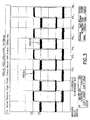
図1の回路は、本発明の一実施形態に従って、双方向半導体スイッチ108および110を用いたハーフブリッジのための駆動回路の第1のトポロジを示す。
The circuit of FIG. 1 illustrates a first topology of a drive circuit for a half bridge using
図1に示すように、2つの双方向半導体素子、具体的には、ハイサイドスイッチ108およびローサイドスイッチ110が、正のDCバスレール(VBUS)と、負すなわち下位のDCバスレールすなわちリターンレール(RTN)との間に直列に配列されている。負荷(図示せず)に接続されることが好ましいハーフブリッジの出力側において、ハイサイドおよびローサイドスイッチ108および110の間に、ノード103が設けられている。
As shown in FIG. 1, two bi-directional semiconductor elements, specifically, a high-
ハーフブリッジのスイッチ108および110を制御するための駆動回路100が設けられている。図1に示した具体的な実施形態では、駆動回路は、2つのフローティングウェル104および106を備えた20Vのバルク基板102上に形成された集積回路(IC)として実現される。第1のウェル(HV1)104は、600Vの容量を有することが好ましく、ハイサイドスイッチ108を駆動するための構成要素を備える。第2のウェル(HV2)106は、20Vの容量を有することが好ましい。
A
ハイサイド双方向スイッチ108は、第1のフローティングウェル104に配置されたトランジスタQ1およびQ2によって形成される従来の出力バッファによって駆動されることが好ましい。図に示すように、トランジスタQ1とQ2との間には、ノード116が配置され、スイッチ108のゲートの1つに接続されている。トランジスタQ1およびQ2のON/OFF状態は、バルクを介して回路100に接続されたハイサイド入力論理制御信号HIに基づいて決定されることが好ましい。IC回路は、従来の駆動回路に共通する適切なレベルシフトおよび遅延の機能をさらに備えることで、ハイサイド入力論理制御信号HIが適切な制御を提供することを保証してもよいことに注意されたい。
The high side
動作中、ハイサイドスイッチ108は、通常はONであるため、ハーフブリッジの出力ノード103を介して負荷に電圧を供給するよう導電する。この時に、トランジスタQ2はOFFであることが好ましく、トランジスタQ1はONであることが好ましい。したがって、スイッチ108のゲートには、電圧が供給されない。スイッチ108は、ノード116に接続されたゲートに電圧が印加されないため、ONのままであり、スイッチ108の他方のゲートにおける電圧は、正のDCバスレールの電圧と同じであることから、いずれのゲートにも負バイアス電圧は掛からない。必要に応じて、スイッチ108は、ハイサイド論理信号HIに基づいてOFFにされてよい。具体的には、スイッチQ2がONにされると共に、スイッチQ1がOFFにされることにより、電圧源109の負端子からトランジスタQ2および高電圧MOSFET114(Mbs)を介して、ノード116に負電圧が供給される。この負電圧は、スイッチ108の下位ゲートに印加されてよく、それにより、このスイッチをOFFにする負バイアスが提供される。
In operation, the high-
従来のハーフブリッジ用の従来の駆動回路と同様に、ハイサイドスイッチ108およびローサイドスイッチ110は、同時にONにならないことが好ましい。したがって、ハイサイドスイッチ108がONである時には、ローサイドスイッチ110はOFFであることが好ましい。同様に、ローサイドスイッチ110がONである時には、ハイサイドスイッチ108はOFFである。したがって、ハイサイド論理入力HIおよびローサイド論理入力LIは、スイッチ108および110が同時にONにならないように供給される。
Similar to the conventional driving circuit for the conventional half bridge, it is preferable that the
このように、ハイサイド論理入力HIがスイッチ108をOFFに駆動した時に、ローサイド論理入力LIは、ローサイドスイッチ110をONにするよう用いられることが好ましい。しかしながら、IC100は、ハイサイドおよびローサイドスイッチ108および110が移行中に同時にONにならないことを保証するために、適切な不感時間(DT)を備えられてもよいことに注意されたい。このように事前に設定された不感時間を用いることは、駆動回路では一般的なことである。ローサイドスイッチ110は、カスコードスイッチングによって制御されることが好ましい。すなわち、電力MOSFET 112は、スイッチ110とDCバスの下位レールとの間に直列で配置される。スイッチ110の上部ゲートは、上部電極に接続されているため、上部電極に対する負バイアスを供給しない。スイッチ110の下部ゲートは、下位のDCバスレールすなわちリターンレールRTNに接続されている。したがって、下位ゲートに印加される電位は、ほぼ一定である。しかしながら、ローサイド入力論理LIは、第2のウェル106のトランジスタQ3およびQ4によって形成された出力バッファを制御するために用いられることが好ましい。この場合にも、ローサイド入力論理LIが適切な制御を提供することを保証するために、適切なレベルシフトおよび遅延が、IC 100に組み込まれてよい。トランジスタQ3およびQ4の間には、ノード118が設けられ、電力MOSFET 11をON/OFFするための電圧を供給する。電力MOSFETがONの時、スイッチのゲートに印加される電位の関係は、スイッチ110がONの状態を保つような関係である。しかしながら、電力MOSFET 110がOFFにされると、スイッチ110のローサイド電極における電圧は、スイッチ110がOFFになるように変化する。
Thus, the low side logic input LI is preferably used to turn on the
図に示すように、ノード118は、さらに、高電圧MOSFET 114を同様に制御し、それによって、電力MOSFET112がONである場合には、高電圧MOSFETはONのみである。特に、電力MOSFET 112をONにする動作と高電圧MOSFETをONにする動作との間にわずかな遅延があることで、電力MOSFET 112がすでにONになった後にのみ、高電圧MOSFET 114がONになることが好ましい。同様に、電力MOSFET 112がOFFになる前に、高電圧MOSFET 114がOFFになることが好ましい。
As shown, the
さらに、電力MOSFET 112が飽和しないことを保証するために、飽和防止制御素子120が設けられる。この特徴は、電力MOSFETの制御の結果として下位のスイッチ110が制御されることを保証するのに望ましい。
In addition, a saturation
IC 100が用いる唯一の外部構成要素は、2つのコンデンサC1およびC2と1つのダイオードD2である。ダイオードD2は、必要に応じてICに組み込まれてもよいことに注意されたい。これは、短絡保護、電流検出、および温度検出を、より容易に提供するために好ましい。
The only external components used by
さらに、図1に示した構成を用いると、コンデンサC1は、ハイサイドスイッチ108がOFFにされた時に、ローサイドスイッチ110、電力MOSFET 112、および高電圧MOSFET 116を介して充電されることが可能であることにも注意されたい。
Further, using the configuration shown in FIG. 1, capacitor C1 can be charged via
図2は、図1に示した回路をシミュレートするために用いられる回路を示す図である。図2の回路は、International Rectifier社が製造するIR2109(4)などのハーフブリッジ駆動チップを用いて、上述の集積回路100の構成要素を実質的に提供する。IR2109(4)の機能およびレイアウトについては、周知であり公開されているため、本明細書では詳細に説明しない。ただし、機能的に等価な他の駆動チップを用いてもよいことを理解されたい。
FIG. 2 is a diagram showing a circuit used for simulating the circuit shown in FIG. The circuit of FIG. 2 substantially provides the components of
図2に示すように、外部コンデンサC1およびC2は、チップの適切なピンの間に接続されている。図2に示したトランジスタM1と、ラベルを付けた高電圧MOSFETは、図1の高電圧MOSFET 114に相当する。双方向半導体スイッチHEMT2およびHEMT1は、図2の双方向スイッチ108および110に相当する。図2に示すさらなる構成要素は、試験に必要な変形および適合を含む。
As shown in FIG. 2, external capacitors C1 and C2 are connected between the appropriate pins of the chip. The transistor M1 shown in FIG. 2 and the labeled high voltage MOSFET correspond to the
図3は、図2のハイサイドおよびローサイドスイッチHEMT2およびHEMT1についてのゲート・ソース電圧(VGS)の測定値を示すグラフである。図に示すように、両方のスイッチのゲート・ソース電圧は、必要に応じて双方向スイッチをON/OFFできるように、正の値と負の値との間を移行する。 FIG. 3 is a graph showing measured values of the gate-source voltage (VGS) for the high-side and low-side switches HEMT2 and HEMT1 of FIG. As shown, the gate-source voltage of both switches transitions between a positive value and a negative value so that the bidirectional switch can be turned on and off as needed.
図4は、図2のハイサイドおよびローサイドスイッチHEMT2およびHEMT1についてのゲート・ソース電圧(VGS)の測定値を示す別のグラフである。図4は、さらに、両方のスイッチがOFFになる図2のスイッチにおけるゲート・ソース電圧の変化の間に提供された不感時間を強調している。さらに、SWNも図示されている。 FIG. 4 is another graph showing measured gate-source voltage (VGS) for the high-side and low-side switches HEMT2 and HEMT1 of FIG. FIG. 4 further highlights the dead time provided during the gate-source voltage change in the switch of FIG. 2 when both switches are OFF. In addition, SWN is also shown.
図5は、基準SWNと共に、図2のローサイドスイッチHEMT1の負荷電流(Iload)、負荷電圧(Vload)、およびゲート・ソース電圧を示すグラフである。 FIG. 5 is a graph showing the load current (Iload), load voltage (Vload), and gate-source voltage of the low-side switch HEMT1 of FIG. 2 together with the reference SWN.
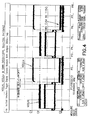
図6は、本発明の別の実施形態に従って、双方向半導体スイッチを用いたハーフブリッジのための駆動回路の第2のトポロジを示す。 FIG. 6 shows a second topology of a drive circuit for a half bridge using a bidirectional semiconductor switch according to another embodiment of the present invention.
図6の回路では、多くの要素が図1の回路と共通しており、共通する要素については、共通の符号を用いている。 In the circuit of FIG. 6, many elements are common to the circuit of FIG. 1, and common symbols are used for the common elements.
図1のように、図6は、2つの双方向半導体素子、具体的には、ハイサイドスイッチ108およびローサイドスイッチ110が、正のDCバスレール(VBUS)と、負すなわち下位のDCバスレールすなわちリターンレール(RTN)との間に直列に配列されている様子を示している。ノード103は、負荷(図示せず)に接続されることが好ましいハーフブリッジの出力側において、ハイサイドおよびローサイドスイッチ108および110の間に設けられている。
As in FIG. 1, FIG. 6 shows that two bidirectional semiconductor devices, specifically, a high-
ハーフブリッジのスイッチ108および110を制御するための駆動回路600が設けられている。図6に示した具体的な実施形態では、駆動回路は、20Vのバルク基板102上に形成された集積回路(IC)と、好ましくは600Vの容量を有すると共にハイサイドスイッチ108を駆動するための構成要素を備える1つのフローティングウェル(HV1)602と、によって実現される。
A
ハイサイド双方向スイッチ108は、第1のフローティングウェル602に配置されたトランジスタQ1およびQ2によって形成される従来の出力バッファによって駆動されることが好ましい。図に示すように、ノード116は、トランジスタQ1とQ2との間に配置され、スイッチ108のゲートの1つに接続されている。トランジスタQ1およびQ2のON/OFF状態は、バルクを介して回路100に接続されたハイサイド入力論理制御信号HIに基づいて決定されることが好ましい。IC回路は、従来の駆動回路に共通する適切なレベルシフトおよび遅延の機能をさらに備えることで、ハイサイド入力論理制御信号HIが適切な制御を提供することを保証してもよいことに注意されたい。
The high side
動作中、ハイサイドスイッチ108は、通常はONであるため、ハーフブリッジの出力ノード103を介して負荷に電圧を供給するよう導電する。この時に、トランジスタQ2はOFFであることが好ましく、トランジスタQ1はONであることが好ましい。したがって、スイッチ108のゲートには、電圧が供給されない。スイッチ108は、ノード116に接続されたゲートに電圧が印加されないため、ONのままであり、スイッチ108の他方のゲートにおける電圧は、正のDCバスレールの電圧と同じであることから、いずれのゲートにも負バイアス電圧は掛からない。
In operation, the high-
さらに、線形レギュレータ制御素子604が、ウェル602に設けられ、コンデンサC23の電圧とスイッチ108の状態とを監視することが好ましい。線形レギュレータ制御素子604は、高電圧トランジスタ606(Mlin)を制御して、トランジスタQ1およびQ2によって形成される出力バッファに電力を供給する。図6に示すように、高電圧トランジスタ606(Mlin)は、p型素子であることが好ましい。コンデンサC23の電圧が、閾値よりも小さくなると(例えば、図6に示した具体的な回路で12ボルトになると)、トランジスタ606は、ONに切り替えられ、それにより、スイッチ108がONであるか否かに関わらず、コンデンサC23を充電するための電流路が確保される。スイッチ108がONの場合、コンデンサC23の電圧が閾値電圧よりも大きければ、トランジスタ606はONにされる。コンデンサC23の電圧が閾値よりも大きい場合には、ノード103における負荷電圧があまりに高く上昇している可能性があり、その場合、スイッチ108をOFFにすることが好ましい。ハイサイド入力論理HIと共に、リターンレール(RTN)の低電圧が、トランジスタ606とトランジスタQ2とを介してノード116に供給され、トランジスタQ2は、論理信号HIによってONにされることが好ましい。ノード116における電圧は、ハイサイドレールおよび出力電圧に対して負となるため、当該電圧はスイッチ108をOFFにする。上述のように、トランジスタQ1がONでトランジスタQ2がOFFである場合には、スイッチ108のゲートには電圧が印加されず、スイッチはONのままである。ハイサイドスイッチ108がOFFでありローサイドスイッチ110および112がONである場合に、コンデンサC23の放電を防止する助けとして、線形レギュレータループ内に低電圧ダイオードD3が設けられてもよい。
Further, a linear
図1に関して上述したように、ローサイド論理入力LIは、必要に応じてローサイドスイッチ110をON/OFFするために用いられることが好ましい。電力MOSFET 112は、スイッチ110とDCバスの下位のレールとの間に直列で配置されてよい。スイッチ110の上部ゲートは、上部電極に接続されているため、上部電極に対する負バイアスを供給しない。スイッチ110の下部ゲートは、下位のDCバスレールすなわちリターンレールRTNに接続されている。したがって、下位のゲートに印加される電位は、ほぼ一定である。しかしながら、ローサイド入力論理LIは、トランジスタQ3およびQ4によって形成された出力バッファを制御するために用いられることが好ましい。ローサイド入力論理LIが適切な制御を提供することを保証するために、適切なレベルシフトおよび遅延が、IC 600に組み込まれてよい。トランジスタQ3およびQ4の間には、ノード118が設けられ、電力MOSFET 112をON/OFFするための電圧を供給する。電力MOSFETがONの時、スイッチのゲートに印加される電位の関係は、スイッチ110がONの状態を保つような関係である。しかしながら、電力MOSFET 110がOFFにされると、スイッチ110のローサイド電極における電圧は、スイッチ110がOFFになるように変化する。
As described above with respect to FIG. 1, the low side logic input LI is preferably used to turn the
電力MOSFET 112が飽和しないことを保証するために、飽和防止制御素子120が設けられてよい。この特徴は、電力MOSFETを制御することにより、下位のスイッチ110が制御されることを保証するのに望ましい。
In order to ensure that the
図6の集積回路600は、図1から外部電力供給109の必要性を排除し、さらに、線形回路への過渡効果を回避することにより、安全な始動と効率的な電圧制御を実現する。
The
図7は、図6の回路を試験するために用いられるシミュレーション回路を示す図である。図8Aから8Cは、図7の回路の様々なパラメータの測定値を示すグラフである。例えば、出力電圧V4のグラフである図8Aに示すように、始動から、出力電圧V4は、滑らかに所望の値まで上昇した後に、所望の値を維持する。 FIG. 7 shows a simulation circuit used to test the circuit of FIG. 8A to 8C are graphs showing measured values of various parameters of the circuit of FIG. For example, as shown in FIG. 8A, which is a graph of the output voltage V4, after starting, the output voltage V4 smoothly rises to a desired value and then maintains the desired value.
図9は、図7のハイサイドおよびローサイドスイッチについてのゲート・ソース電圧(VGS)の測定値を示すグラフである。図からわかるように、ゲート・ソース電圧は、正と負の値を交互に取るため、必要な時にスイッチをOFFにするのに十分である。さらに、図7の回路のSWNが図示されている。 FIG. 9 is a graph showing measured values of gate-source voltage (VGS) for the high-side and low-side switches of FIG. As can be seen, the gate-source voltage takes alternating positive and negative values and is sufficient to turn the switch off when needed. Furthermore, the SWN of the circuit of FIG. 7 is shown.
本発明は、具体的な実施形態に関連して説明されているが、多くの他の変更例および変形例、他の用途が存在することは、当業者にとって明らかなことである。したがって、本発明は、本明細書の具体的な開示によって限定されず、添付の特許請求の範囲によってのみ限定されることが好ましい。 Although the present invention has been described in connection with specific embodiments, it will be apparent to those skilled in the art that many other modifications and variations and other applications exist. Accordingly, the invention is preferably not limited by the specific disclosure herein, but only by the scope of the appended claims.
Claims (18)
ハイサイド双方向半導体スイッチを制御するよう動作可能なハイサイド駆動部であって、前記ハイサイド双方向半導体スイッチに負バイアス電圧を供給して前記ハイサイド双方向半導体スイッチをOFFにするハイサイド駆動部と、
ローサイド双方向半導体スイッチを制御するよう動作可能なローサイド駆動部と、
負端子が前記ハイサイド駆動部に接続された外部電圧源と、
前記電圧源の前記負端子と前記ハイサイド駆動部との間に配置され、前記ローサイド駆動部が前記ローサイド双方向半導体スイッチをONにする時に、前記ハイサイド駆動部を前記電圧源の前記負端子に接続するよう動作可能なハイサイド駆動スイッチと、を備える、駆動回路。 A driving circuit for a half bridge using a bidirectional semiconductor switch,
A high-side drive unit operable to control a high-side bidirectional semiconductor switch, wherein the high-side bidirectional semiconductor switch is turned off by supplying a negative bias voltage to the high-side bidirectional semiconductor switch And
A low side driver operable to control the low side bidirectional semiconductor switch; and
An external voltage source having a negative terminal connected to the high side driver;
The high-side driver is disposed between the negative terminal of the voltage source and the high-side driver, and when the low-side driver turns on the low-side bidirectional semiconductor switch, the high-side driver is connected to the negative terminal of the voltage source. And a high-side drive switch operable to connect to the drive circuit.
前記ハイサイド駆動部は、ハイサイド入力制御信号によって制御される、駆動回路。 The drive circuit according to claim 1,
The high-side drive unit is a drive circuit controlled by a high-side input control signal.
前記ローサイド駆動部は、ローサイド入力制御信号によって制御される、駆動回路。 The drive circuit according to claim 1,
The low-side drive unit is a drive circuit controlled by a low-side input control signal.
前記ローサイド駆動部は、さらに、
プッシュプル構成として配置されていると共に、前記ローサイド入力制御信号に基づいてONおよびOFFに切り替えられる第1のトランジスタおよび第2のトランジスタと、
前記ローサイド双方向半導体スイッチと直列に配置された電力MOSFETと、
前記第1および第2のトランジスタの間に配置され、前記電力MOSFETのゲートに接続された出力ノードと、を備え、
前記出力ノードの電圧値が前記電力MOSFETをONにする時には、前記ローサイド双方向半導体スイッチがONであり、前記出力ノードの電圧値が前記電力MOSFETをOFFにする時には、前記ローサイド双方向半導体スイッチがOFFである、駆動回路。 The drive circuit according to claim 3,
The low side driving unit further includes:
A first transistor and a second transistor arranged as a push-pull configuration and switched on and off based on the low side input control signal;
A power MOSFET disposed in series with the low-side bidirectional semiconductor switch;
An output node disposed between the first and second transistors and connected to a gate of the power MOSFET;
When the voltage value of the output node turns on the power MOSFET, the low-side bidirectional semiconductor switch is ON, and when the voltage value of the output node turns off the power MOSFET, the low-side bidirectional semiconductor switch A drive circuit that is OFF.
前記ローサイド駆動部は、さらに、前記電力MOSFETに接続された飽和防止制御素子を備えることで、前記電力MOSFEが飽和状態で動作しないことを保証する、駆動回路。 The drive circuit according to claim 4,
The low-side drive unit further includes a saturation prevention control element connected to the power MOSFET, thereby ensuring that the power MOSFE does not operate in a saturated state.
前記ローサイド入力制御信号は、さらに、前記ローサイド双方向半導体スイッチがONにされた時に前記電圧源の前記負端子が前記ハイサイド駆動部に接続されるように、前記ハイサイド駆動スイッチを制御し、
前記負端子の負電圧は、前記ハイサイド双方向半導体スイッチをOFFにするために用いられる、駆動回路。 The drive circuit according to claim 3,
The low-side input control signal further controls the high-side drive switch so that the negative terminal of the voltage source is connected to the high-side drive when the low-side bidirectional semiconductor switch is turned on;
The drive circuit, wherein the negative voltage at the negative terminal is used to turn off the high-side bidirectional semiconductor switch.
ハイサイド双方向半導体スイッチを制御するよう動作可能なハイサイド駆動部であって、前記ハイサイド駆動部を前記ハーフブリッジの下位レールに選択的に接続する線形レギュレータ制御装置を含むハイサイド駆動部と、
ローサイド双方向半導体スイッチを制御するよう動作可能なローサイド駆動部と、を備える、駆動回路。 A driving circuit for a half bridge using a bidirectional semiconductor switch,
A high side driver operable to control a high side bidirectional semiconductor switch, the high side driver including a linear regulator controller that selectively connects the high side driver to a lower rail of the half bridge; ,
And a low-side drive unit operable to control the low-side bidirectional semiconductor switch.
前記線形レギュレータ制御装置は、前記ハイサイド双方向スイッチがONであり、かつ、前記ハイサイド駆動部を横切るコンデンサの電圧が閾値電圧よりも高くなった時に、前記ハイサイド駆動部を前記ハーフブリッジの前記下位レールに接続し、それにより、前記ハイサイド駆動部は、前記ハイサイド双方向半導体素子のゲートに負バイアス電圧を印可して、前記ハイサイド双方向半導体素子をOFFにする、駆動回路。 The drive circuit according to claim 7,
In the linear regulator control device, when the high-side bidirectional switch is ON and the voltage of the capacitor across the high-side drive unit becomes higher than a threshold voltage, the high-side drive unit is connected to the half bridge. A drive circuit connected to the lower rail, whereby the high-side driver applies a negative bias voltage to the gate of the high-side bidirectional semiconductor element to turn off the high-side bidirectional semiconductor element.
前記線形レギュレータ制御装置は、前記コンデンサの前記電圧が前記閾値よりも低くなった時に、前記ハイサイド駆動部を前記ハーフブリッジの前記下位レールに接続する、駆動回路。 The drive circuit according to claim 8, wherein
The linear regulator control device is a drive circuit that connects the high-side drive unit to the lower rail of the half bridge when the voltage of the capacitor becomes lower than the threshold.
前記ローサイド駆動部は、さらに、
プッシュプル構成として配置されていると共に、前記ローサイド入力制御信号に基づいてONおよびOFFに切り替えられる第1のトランジスタおよび第2のトランジスタと、
前記ローサイド双方向半導体スイッチと直列に配置された電力MOSFETと、
前記第1および第2のトランジスタの間に配置され、前記電力MOSFETのゲートに接続された出力ノードと、を備え、
前記出力ノードの電圧値が前記電力MOSFETをONにする時には、前記ローサイド双方向半導体スイッチがONであり、前記出力ノードの電圧値が前記電力MOSFETをOFFにする時には、前記ローサイド双方向半導体スイッチがOFFである、駆動回路。 The drive circuit according to claim 7,
The low side driving unit further includes:
A first transistor and a second transistor arranged as a push-pull configuration and switched on and off based on the low side input control signal;
A power MOSFET disposed in series with the low-side bidirectional semiconductor switch;
An output node disposed between the first and second transistors and connected to a gate of the power MOSFET;
When the voltage value of the output node turns on the power MOSFET, the low-side bidirectional semiconductor switch is ON, and when the voltage value of the output node turns off the power MOSFET, the low-side bidirectional semiconductor switch A drive circuit that is OFF.
前記ローサイド駆動部は、さらに、前記電力MOSFETに接続された飽和防止制御素子を備えることで、前記電力MOSFEが飽和状態で動作しないことを保証する、駆動回路。 The drive circuit according to claim 10, comprising:
The low-side drive unit further includes a saturation prevention control element connected to the power MOSFET, thereby ensuring that the power MOSFE does not operate in a saturated state.
ハイサイド双方向半導体スイッチと、
前記ハイサイド双方向半導体スイッチと直列に接続されたローサイド双方向半導体スイッチと、
請求項7に記載の駆動回路と、を備える、双方向スイッチング回路。 A bidirectional switching circuit,
A high-side bidirectional semiconductor switch,
A low-side bidirectional semiconductor switch connected in series with the high-side bidirectional semiconductor switch;
A bidirectional switching circuit comprising: the drive circuit according to claim 7.
ハイサイド双方向半導体スイッチと、
前記ハイサイド双方向半導体スイッチと直列に接続されたローサイド双方向半導体スイッチと、
前記ハイサイド双方向半導体スイッチを制御するよう動作可能なハイサイド駆動部であって、前記ハイサイド双方向半導体スイッチに負バイアス電圧を供給して前記ハイサイド双方向半導体スイッチをOFFにするハイサイド駆動部と、
前記ローサイド双方向半導体スイッチを制御するよう動作可能なローサイド駆動部と、
負端子が前記ハイサイド駆動部に接続された外部電圧源と、
前記電圧源の前記負端子と前記ハイサイド駆動部との間に配置され、前記ローサイド駆動部が前記ローサイド双方向半導体スイッチをONにする時に、前記ハイサイド駆動部を前記電圧源の前記負端子に接続するよう動作可能なハイサイド駆動スイッチと、を備える、双方向スイッチング回路。 A bidirectional switching circuit,
A high-side bidirectional semiconductor switch,
A low-side bidirectional semiconductor switch connected in series with the high-side bidirectional semiconductor switch;
A high-side driver operable to control the high-side bidirectional semiconductor switch, wherein the high-side bidirectional semiconductor switch is turned off by supplying a negative bias voltage to the high-side bidirectional semiconductor switch. A drive unit;
A low side driver operable to control the low side bidirectional semiconductor switch;
An external voltage source having a negative terminal connected to the high side driver;
The high-side driver is disposed between the negative terminal of the voltage source and the high-side driver, and when the low-side driver turns on the low-side bidirectional semiconductor switch, the high-side driver is connected to the negative terminal of the voltage source. And a high-side drive switch operable to connect to the bidirectional switching circuit.
前記ハイサイド駆動部は、ハイサイド入力制御信号によって制御される、双方向スイッチング回路。 A bidirectional switching circuit according to claim 13, comprising:
The high side driving unit is a bidirectional switching circuit controlled by a high side input control signal.
前記ローサイド駆動部は、ローサイド入力制御信号によって制御される、双方向スイッチング回路。 A bidirectional switching circuit according to claim 13, comprising:
The low side driver is a bidirectional switching circuit controlled by a low side input control signal.
前記ローサイド駆動部は、さらに、
プッシュプル構成として配置されていると共に、前記ローサイド入力制御信号に基づいてONおよびOFFに切り替えられる第1のトランジスタおよび第2のトランジスタと、
前記ローサイド双方向半導体スイッチと直列に配置された電力MOSFETと、
前記第1および第2のトランジスタの間に配置され、前記電力MOSFETのゲートに接続された出力ノードと、を備え、
前記出力ノードの電圧値が前記電力MOSFETをONにする時には、前記ローサイド双方向半導体スイッチがONであり、前記出力ノードの電圧値が前記電力MOSFETをOFFにする時には、前記ローサイド双方向半導体スイッチがOFFである、双方向スイッチング回路。 The bidirectional switching circuit according to claim 15, wherein
The low side driving unit further includes:
A first transistor and a second transistor arranged as a push-pull configuration and switched on and off based on the low side input control signal;
A power MOSFET disposed in series with the low-side bidirectional semiconductor switch;
An output node disposed between the first and second transistors and connected to a gate of the power MOSFET;
When the voltage value of the output node turns on the power MOSFET, the low-side bidirectional semiconductor switch is ON, and when the voltage value of the output node turns off the power MOSFET, the low-side bidirectional semiconductor switch Bidirectional switching circuit that is OFF.
前記ローサイド駆動部は、さらに、前記電力MOSFETに接続された飽和防止制御素子を備えることで、前記電力MOSFEが飽和状態で動作しないことを保証する、双方向スイッチング回路。 The bidirectional switching circuit according to claim 16, comprising:
The low-side driver further includes a saturation prevention control element connected to the power MOSFET, thereby ensuring that the power MOSFE does not operate in a saturated state.
前記ローサイド入力制御信号は、さらに、前記ローサイド双方向半導体スイッチがONにされた時に前記電圧源の前記負端子が前記ハイサイド駆動部に接続されるように、前記ハイサイド駆動スイッチを制御し、
前記負端子の負電圧は、前記ハイサイド双方向半導体スイッチをOFFにするために用いられる、双方向スイッチング素子。 The bidirectional switching element according to claim 17,
The low-side input control signal further controls the high-side drive switch so that the negative terminal of the voltage source is connected to the high-side drive when the low-side bidirectional semiconductor switch is turned on;
The bidirectional switching element, wherein the negative voltage of the negative terminal is used to turn off the high-side bidirectional semiconductor switch.
Applications Claiming Priority (3)
| Application Number | Priority Date | Filing Date | Title |
|---|---|---|---|
| US67082905P | 2005-04-13 | 2005-04-13 | |
| US68062905P | 2005-05-13 | 2005-05-13 | |
| US11/402,109 US7928702B2 (en) | 2005-04-13 | 2006-04-11 | Driving circuit for use with high voltage depletion-mode semiconductor switches |
Publications (2)
| Publication Number | Publication Date |
|---|---|
| JP2006352839A true JP2006352839A (en) | 2006-12-28 |
| JP2006352839A5 JP2006352839A5 (en) | 2008-12-11 |
Family
ID=37295568
Family Applications (1)
| Application Number | Title | Priority Date | Filing Date |
|---|---|---|---|
| JP2006110890A Ceased JP2006352839A (en) | 2005-04-13 | 2006-04-13 | Driving circuit for high-voltage bidirectional semiconductor switch |
Country Status (4)
| Country | Link |
|---|---|
| US (2) | US7928702B2 (en) |
| JP (1) | JP2006352839A (en) |
| DE (1) | DE102006017242A1 (en) |
| TW (1) | TW200644396A (en) |
Cited By (3)
| Publication number | Priority date | Publication date | Assignee | Title |
|---|---|---|---|---|
| JP2010124584A (en) * | 2008-11-19 | 2010-06-03 | Panasonic Corp | Motor control device |
| JP2010239765A (en) * | 2009-03-31 | 2010-10-21 | Panasonic Corp | Motor drive device |
| JP2014204354A (en) * | 2013-04-08 | 2014-10-27 | 富士通セミコンダクター株式会社 | Drive circuit, semiconductor integrated circuit, and control method for drive circuit |
Families Citing this family (15)
| Publication number | Priority date | Publication date | Assignee | Title |
|---|---|---|---|---|
| JP2006223016A (en) * | 2005-02-08 | 2006-08-24 | Renesas Technology Corp | Power supply system, multi-chip module, system-in-package, and non-isolated dc-dc converter |
| US8063613B2 (en) * | 2006-12-11 | 2011-11-22 | International Rectifier Corporation | Power converter driver with split power supply |
| US7863877B2 (en) * | 2006-12-11 | 2011-01-04 | International Rectifier Corporation | Monolithically integrated III-nitride power converter |
| US8659275B2 (en) * | 2008-01-11 | 2014-02-25 | International Rectifier Corporation | Highly efficient III-nitride power conversion circuit |
| US8063616B2 (en) * | 2008-01-11 | 2011-11-22 | International Rectifier Corporation | Integrated III-nitride power converter circuit |
| KR20100056244A (en) * | 2008-11-19 | 2010-05-27 | 페어차일드코리아반도체 주식회사 | Switch driving circuit and switch driving method |
| FR2998735B1 (en) | 2012-11-27 | 2022-10-07 | Hispano Suiza Sa | HIGH VOLTAGE DC-DC VOLTAGE CONVERTER |
| JP6113542B2 (en) * | 2013-03-21 | 2017-04-12 | 株式会社東芝 | Semiconductor device |
| US9985626B2 (en) * | 2015-01-30 | 2018-05-29 | Navitas Semiconductor, Inc. | Bidirectional GaN switch with built-in bias supply and integrated gate drivers |
| US10205313B2 (en) | 2015-07-24 | 2019-02-12 | Symptote Technologies, LLC | Two-transistor devices for protecting circuits from sustained overcurrent |
| CN108292837B (en) | 2015-09-21 | 2020-01-17 | 西普托特技术有限责任公司 | Single transistor device and method for protecting a circuit |
| TWI563488B (en) | 2016-02-01 | 2016-12-21 | Sitronix Technology Corp | Gate driving circuit |
| US20170294848A1 (en) * | 2016-04-07 | 2017-10-12 | Visic Technologies Ltd. | Method and device for ac fed switch mode power supply based on normally on transistors |
| US10122362B2 (en) * | 2017-04-11 | 2018-11-06 | Infineon Technologies Austria Ag | Dynamic biasing circuitry for level-shifter circuitry |
| US11004942B2 (en) * | 2017-12-30 | 2021-05-11 | Texas Instruments Incorporated | Controlling bi-directional switching devices |
Family Cites Families (9)
| Publication number | Priority date | Publication date | Assignee | Title |
|---|---|---|---|---|
| DE19931059C2 (en) * | 1999-07-06 | 2002-04-18 | Texas Instruments Deutschland | DC converter |
| US6989659B2 (en) * | 2002-09-09 | 2006-01-24 | Acutechnology Semiconductor | Low dropout voltage regulator using a depletion pass transistor |
| US7026797B2 (en) * | 2003-03-21 | 2006-04-11 | Tropian, Inc. | Extremely high-speed switchmode DC-DC converters |
| US7385375B2 (en) * | 2005-02-23 | 2008-06-10 | Coldwatt, Inc. | Control circuit for a depletion mode switch and method of operating the same |
| GB2432471A (en) * | 2005-11-01 | 2007-05-23 | Zetex Semiconductors Plc | A CMOS support IC for a DBS LNA |
| US20080186004A1 (en) * | 2005-11-29 | 2008-08-07 | Advanced Analogic Technologies, Inc. | High-Frequency Power MESFET Boost Switching Power Supply |
| US20070170897A1 (en) * | 2006-01-26 | 2007-07-26 | Advanced Analogic Technologies, Inc. | High-Frequency Power MESFET Buck Switching Power Supply |
| US7863877B2 (en) * | 2006-12-11 | 2011-01-04 | International Rectifier Corporation | Monolithically integrated III-nitride power converter |
| JP2008235952A (en) * | 2007-03-16 | 2008-10-02 | Furukawa Electric Co Ltd:The | Driving circuit for depletion type switching element |
-
2006
- 2006-04-11 US US11/402,109 patent/US7928702B2/en not_active Expired - Fee Related
- 2006-04-12 TW TW095112977A patent/TW200644396A/en unknown
- 2006-04-12 DE DE102006017242A patent/DE102006017242A1/en not_active Withdrawn
- 2006-04-13 JP JP2006110890A patent/JP2006352839A/en not_active Ceased
-
2011
- 2011-04-07 US US13/081,744 patent/US8193786B2/en not_active Expired - Fee Related
Cited By (3)
| Publication number | Priority date | Publication date | Assignee | Title |
|---|---|---|---|---|
| JP2010124584A (en) * | 2008-11-19 | 2010-06-03 | Panasonic Corp | Motor control device |
| JP2010239765A (en) * | 2009-03-31 | 2010-10-21 | Panasonic Corp | Motor drive device |
| JP2014204354A (en) * | 2013-04-08 | 2014-10-27 | 富士通セミコンダクター株式会社 | Drive circuit, semiconductor integrated circuit, and control method for drive circuit |
Also Published As
| Publication number | Publication date |
|---|---|
| US20060279351A1 (en) | 2006-12-14 |
| TW200644396A (en) | 2006-12-16 |
| DE102006017242A1 (en) | 2006-11-16 |
| US20110181252A1 (en) | 2011-07-28 |
| US8193786B2 (en) | 2012-06-05 |
| US7928702B2 (en) | 2011-04-19 |
Similar Documents
| Publication | Publication Date | Title |
|---|---|---|
| JP2006352839A (en) | Driving circuit for high-voltage bidirectional semiconductor switch | |
| US8183715B2 (en) | Reverse current preventing circuit and power source switching apparatus | |
| JP5315026B2 (en) | Semiconductor device | |
| US8729566B2 (en) | Semiconductor switching arrangement having a normally on and a normally off transistor | |
| US7948220B2 (en) | Method and apparatus to reduce dynamic Rdson in a power switching circuit having a III-nitride device | |
| US8564359B2 (en) | Method and system for controlling HS-NMOS power switches with slew-rate limitation | |
| CN107852159B (en) | Drive device | |
| JP2008187885A (en) | Synchronous dc/dc converter | |
| US11201613B2 (en) | Driver circuit and method of operating the same | |
| US20140266322A1 (en) | Driver circuit with controlled gate discharge current | |
| JP6417546B2 (en) | Gate drive circuit and power converter using the same | |
| KR20130029337A (en) | Semiconductor device | |
| US6979981B2 (en) | DC-DC converter control circuit and DC-DC converter | |
| US9059697B2 (en) | Drive circuit and drive method for driving normally-on-type transistor | |
| US9595947B2 (en) | Driver device for transistors, and corresponding integrated circuit | |
| KR20040029082A (en) | Half-bridge circuit | |
| JP4830829B2 (en) | Insulated gate transistor drive circuit | |
| JP2020096444A (en) | Switching circuit | |
| US11349474B1 (en) | Cascaded gate driver outputs for power conversion circuits | |
| US11677393B2 (en) | Driver circuit and method of operating the same | |
| JP2005143282A (en) | Step-down pwm converter | |
| CN114303309A (en) | Overcurrent protection circuit and switch circuit | |
| WO2021246044A1 (en) | Switching device circuit, switching system, and switching device processing method | |
| KR20230150228A (en) | Method for operating a power transistor circuit | |
| JP2010147544A (en) | Driving device |
Legal Events
| Date | Code | Title | Description |
|---|---|---|---|
| A521 | Request for written amendment filed |
Free format text: JAPANESE INTERMEDIATE CODE: A523 Effective date: 20081028 |
|
| A977 | Report on retrieval |
Free format text: JAPANESE INTERMEDIATE CODE: A971007 Effective date: 20081125 |
|
| A01 | Written decision to grant a patent or to grant a registration (utility model) |
Free format text: JAPANESE INTERMEDIATE CODE: A01 Effective date: 20090113 |
|
| A045 | Written measure of dismissal of application [lapsed due to lack of payment] |
Free format text: JAPANESE INTERMEDIATE CODE: A045 Effective date: 20090526 |