JP2006350342A - Display device and apparatus for driving display device - Google Patents
Display device and apparatus for driving display device Download PDFInfo
- Publication number
- JP2006350342A JP2006350342A JP2006162120A JP2006162120A JP2006350342A JP 2006350342 A JP2006350342 A JP 2006350342A JP 2006162120 A JP2006162120 A JP 2006162120A JP 2006162120 A JP2006162120 A JP 2006162120A JP 2006350342 A JP2006350342 A JP 2006350342A
- Authority
- JP
- Japan
- Prior art keywords
- output video
- video signal
- signal
- display device
- gradation
- Prior art date
- Legal status (The legal status is an assumption and is not a legal conclusion. Google has not performed a legal analysis and makes no representation as to the accuracy of the status listed.)
- Withdrawn
Links
- 239000011159 matrix material Substances 0.000 claims abstract description 5
- 230000006870 function Effects 0.000 claims description 7
- 239000004973 liquid crystal related substance Substances 0.000 description 49
- 238000002834 transmittance Methods 0.000 description 19
- 239000003990 capacitor Substances 0.000 description 15
- 238000010586 diagram Methods 0.000 description 9
- 238000000034 method Methods 0.000 description 8
- 230000008859 change Effects 0.000 description 7
- 239000003086 colorant Substances 0.000 description 6
- 230000000694 effects Effects 0.000 description 6
- 230000001276 controlling effect Effects 0.000 description 3
- 230000005684 electric field Effects 0.000 description 3
- 230000004044 response Effects 0.000 description 3
- 239000010409 thin film Substances 0.000 description 3
- 230000005540 biological transmission Effects 0.000 description 2
- 230000006866 deterioration Effects 0.000 description 2
- 239000010408 film Substances 0.000 description 2
- 239000012212 insulator Substances 0.000 description 2
- 230000010287 polarization Effects 0.000 description 2
- 230000008569 process Effects 0.000 description 2
- 230000001105 regulatory effect Effects 0.000 description 2
- 206010047571 Visual impairment Diseases 0.000 description 1
- 230000015556 catabolic process Effects 0.000 description 1
- 125000004122 cyclic group Chemical group 0.000 description 1
- 230000007423 decrease Effects 0.000 description 1
- 238000006731 degradation reaction Methods 0.000 description 1
- 238000012986 modification Methods 0.000 description 1
- 230000004048 modification Effects 0.000 description 1
- 239000003607 modifier Substances 0.000 description 1
- 238000013139 quantization Methods 0.000 description 1
- 230000002123 temporal effect Effects 0.000 description 1
Images


Classifications
-
- G—PHYSICS
- G09—EDUCATION; CRYPTOGRAPHY; DISPLAY; ADVERTISING; SEALS
- G09G—ARRANGEMENTS OR CIRCUITS FOR CONTROL OF INDICATING DEVICES USING STATIC MEANS TO PRESENT VARIABLE INFORMATION
- G09G3/00—Control arrangements or circuits, of interest only in connection with visual indicators other than cathode-ray tubes
- G09G3/20—Control arrangements or circuits, of interest only in connection with visual indicators other than cathode-ray tubes for presentation of an assembly of a number of characters, e.g. a page, by composing the assembly by combination of individual elements arranged in a matrix no fixed position being assigned to or needed to be assigned to the individual characters or partial characters
- G09G3/34—Control arrangements or circuits, of interest only in connection with visual indicators other than cathode-ray tubes for presentation of an assembly of a number of characters, e.g. a page, by composing the assembly by combination of individual elements arranged in a matrix no fixed position being assigned to or needed to be assigned to the individual characters or partial characters by control of light from an independent source
- G09G3/36—Control arrangements or circuits, of interest only in connection with visual indicators other than cathode-ray tubes for presentation of an assembly of a number of characters, e.g. a page, by composing the assembly by combination of individual elements arranged in a matrix no fixed position being assigned to or needed to be assigned to the individual characters or partial characters by control of light from an independent source using liquid crystals
- G09G3/3611—Control of matrices with row and column drivers
- G09G3/3685—Details of drivers for data electrodes
- G09G3/3688—Details of drivers for data electrodes suitable for active matrices only
-
- G—PHYSICS
- G09—EDUCATION; CRYPTOGRAPHY; DISPLAY; ADVERTISING; SEALS
- G09G—ARRANGEMENTS OR CIRCUITS FOR CONTROL OF INDICATING DEVICES USING STATIC MEANS TO PRESENT VARIABLE INFORMATION
- G09G3/00—Control arrangements or circuits, of interest only in connection with visual indicators other than cathode-ray tubes
- G09G3/20—Control arrangements or circuits, of interest only in connection with visual indicators other than cathode-ray tubes for presentation of an assembly of a number of characters, e.g. a page, by composing the assembly by combination of individual elements arranged in a matrix no fixed position being assigned to or needed to be assigned to the individual characters or partial characters
- G09G3/34—Control arrangements or circuits, of interest only in connection with visual indicators other than cathode-ray tubes for presentation of an assembly of a number of characters, e.g. a page, by composing the assembly by combination of individual elements arranged in a matrix no fixed position being assigned to or needed to be assigned to the individual characters or partial characters by control of light from an independent source
- G09G3/36—Control arrangements or circuits, of interest only in connection with visual indicators other than cathode-ray tubes for presentation of an assembly of a number of characters, e.g. a page, by composing the assembly by combination of individual elements arranged in a matrix no fixed position being assigned to or needed to be assigned to the individual characters or partial characters by control of light from an independent source using liquid crystals
-
- G—PHYSICS
- G02—OPTICS
- G02F—OPTICAL DEVICES OR ARRANGEMENTS FOR THE CONTROL OF LIGHT BY MODIFICATION OF THE OPTICAL PROPERTIES OF THE MEDIA OF THE ELEMENTS INVOLVED THEREIN; NON-LINEAR OPTICS; FREQUENCY-CHANGING OF LIGHT; OPTICAL LOGIC ELEMENTS; OPTICAL ANALOGUE/DIGITAL CONVERTERS
- G02F1/00—Devices or arrangements for the control of the intensity, colour, phase, polarisation or direction of light arriving from an independent light source, e.g. switching, gating or modulating; Non-linear optics
- G02F1/01—Devices or arrangements for the control of the intensity, colour, phase, polarisation or direction of light arriving from an independent light source, e.g. switching, gating or modulating; Non-linear optics for the control of the intensity, phase, polarisation or colour
- G02F1/13—Devices or arrangements for the control of the intensity, colour, phase, polarisation or direction of light arriving from an independent light source, e.g. switching, gating or modulating; Non-linear optics for the control of the intensity, phase, polarisation or colour based on liquid crystals, e.g. single liquid crystal display cells
- G02F1/133—Constructional arrangements; Operation of liquid crystal cells; Circuit arrangements
-
- G—PHYSICS
- G09—EDUCATION; CRYPTOGRAPHY; DISPLAY; ADVERTISING; SEALS
- G09G—ARRANGEMENTS OR CIRCUITS FOR CONTROL OF INDICATING DEVICES USING STATIC MEANS TO PRESENT VARIABLE INFORMATION
- G09G3/00—Control arrangements or circuits, of interest only in connection with visual indicators other than cathode-ray tubes
- G09G3/20—Control arrangements or circuits, of interest only in connection with visual indicators other than cathode-ray tubes for presentation of an assembly of a number of characters, e.g. a page, by composing the assembly by combination of individual elements arranged in a matrix no fixed position being assigned to or needed to be assigned to the individual characters or partial characters
- G09G3/34—Control arrangements or circuits, of interest only in connection with visual indicators other than cathode-ray tubes for presentation of an assembly of a number of characters, e.g. a page, by composing the assembly by combination of individual elements arranged in a matrix no fixed position being assigned to or needed to be assigned to the individual characters or partial characters by control of light from an independent source
- G09G3/36—Control arrangements or circuits, of interest only in connection with visual indicators other than cathode-ray tubes for presentation of an assembly of a number of characters, e.g. a page, by composing the assembly by combination of individual elements arranged in a matrix no fixed position being assigned to or needed to be assigned to the individual characters or partial characters by control of light from an independent source using liquid crystals
- G09G3/3611—Control of matrices with row and column drivers
- G09G3/3696—Generation of voltages supplied to electrode drivers
-
- G—PHYSICS
- G09—EDUCATION; CRYPTOGRAPHY; DISPLAY; ADVERTISING; SEALS
- G09G—ARRANGEMENTS OR CIRCUITS FOR CONTROL OF INDICATING DEVICES USING STATIC MEANS TO PRESENT VARIABLE INFORMATION
- G09G2320/00—Control of display operating conditions
- G09G2320/02—Improving the quality of display appearance
- G09G2320/0285—Improving the quality of display appearance using tables for spatial correction of display data
-
- G—PHYSICS
- G09—EDUCATION; CRYPTOGRAPHY; DISPLAY; ADVERTISING; SEALS
- G09G—ARRANGEMENTS OR CIRCUITS FOR CONTROL OF INDICATING DEVICES USING STATIC MEANS TO PRESENT VARIABLE INFORMATION
- G09G2320/00—Control of display operating conditions
- G09G2320/06—Adjustment of display parameters
- G09G2320/0673—Adjustment of display parameters for control of gamma adjustment, e.g. selecting another gamma curve
-
- G—PHYSICS
- G09—EDUCATION; CRYPTOGRAPHY; DISPLAY; ADVERTISING; SEALS
- G09G—ARRANGEMENTS OR CIRCUITS FOR CONTROL OF INDICATING DEVICES USING STATIC MEANS TO PRESENT VARIABLE INFORMATION
- G09G2360/00—Aspects of the architecture of display systems
- G09G2360/18—Use of a frame buffer in a display terminal, inclusive of the display panel
Abstract
Description
本発明は表示装置及び表示装置の駆動装置に関する。 The present invention relates to a display device and a drive device for the display device.
一般的な液晶表示装置(liquid crystal display、LCD)は、画素電極及び共通電極を備える2つの表示板と、その間に入っている誘電率異方性(dielectric anisotropy)を有する液晶層とを含む。画素電極は行列状に配列され、薄膜トランジスタ(TFT)などスイッチング素子に接続されており、1つの行毎に順にデータ信号の印加を受ける。共通電極は画素電極と異なる表示板または同じ表示板に設けられ、共通電圧の印加を受ける。画素電極と共通電極及びその間の液晶層は、回路的に見れば液晶キャパシタをなし、液晶キャパシタはこれに接続されたスイッチング素子と共に画素を構成する基本単位となる。 A typical liquid crystal display (LCD) includes two display panels including a pixel electrode and a common electrode, and a liquid crystal layer having a dielectric anisotropy interposed therebetween. The pixel electrodes are arranged in a matrix and are connected to a switching element such as a thin film transistor (TFT), and are sequentially applied with a data signal for each row. The common electrode is provided on a display panel different from the pixel electrode or on the same display panel and receives a common voltage. The pixel electrode, the common electrode, and the liquid crystal layer between them constitute a liquid crystal capacitor in terms of a circuit, and the liquid crystal capacitor is a basic unit constituting a pixel together with a switching element connected thereto.
このような液晶表示装置においては、2つの電極に電圧を印加して液晶層に電界を生成し、この電界の強さを調節して液晶層を通過する光の透過率を調節することによって所望の画像を得る。この時、液晶層に一方向の電界が永らく印加されることによって発生する劣化現象やフリッカーなどを防止するために、フレーム別に、行別に、または画素別に共通電圧に対するデータ信号の電圧極性を反転させる。 In such a liquid crystal display device, a voltage is applied to two electrodes to generate an electric field in the liquid crystal layer, and the intensity of this electric field is adjusted to adjust the transmittance of light passing through the liquid crystal layer. Get the image. At this time, the voltage polarity of the data signal with respect to the common voltage is inverted for each frame, for each row, or for each pixel in order to prevent a deterioration phenomenon or flicker caused by a unidirectional electric field applied to the liquid crystal layer. .
ところが、このようにデータ信号の電圧極性を反転させる場合、液晶分子の応答速度が遅くて液晶キャパシタが目標電圧に充電されるまで時間が長くかかり、画面が鮮明でなくぼやける(blurring)現象が発生し、特に、動映像である場合、映像変化が速かに行われず所望の映像に速く変わらないなどの問題が現れる。
このような問題を解決するために、短時間の間にブラック画面を挿入するインパルシブ(impulsive)駆動方式が開発された。
However, when the voltage polarity of the data signal is inverted in this way, the response speed of the liquid crystal molecules is slow and it takes a long time until the liquid crystal capacitor is charged to the target voltage, and the screen is not clear and blurring occurs. In particular, in the case of a moving image, there is a problem that the image does not change quickly and does not change quickly to a desired image.
In order to solve such a problem, an impulsive driving method in which a black screen is inserted in a short time has been developed.
このようなインパルシブ駆動方式は、一定の周期でバックライトランプを消して画面全体をブラックにする方式(impulsive emission type)と、実質的に表示に関与する正常データ信号の他に一定の周期でブラックデータ信号を画素に印加する方式(cyclic resetting type)がある。
しかし、インパルシブ駆動方式の場合、決められた時間間隔でブラック表示を行う画面が挿入されるので画面の輝度が落ちる。
Such an impulsive drive method is a method in which the backlight lamp is turned off at a constant cycle to make the entire screen black (impulsive emission type), and in addition to a normal data signal that is substantially involved in display, a black signal at a fixed cycle. There is a method of applying a data signal to a pixel (cyclic resetting type).
However, in the case of the impulsive driving method, since a screen for black display is inserted at a predetermined time interval, the brightness of the screen is lowered.
そこで、本発明が目的とする技術的課題は、表示装置の輝度を高めながら画質を改善することにある。
また、本発明が目的とする他の技術的課題は、動映像の画質を改善することにある。
Therefore, the technical problem aimed at by the present invention is to improve the image quality while increasing the luminance of the display device.
Another technical problem to be solved by the present invention is to improve the quality of moving images.
本発明の特徴による表示装置は、行列状に配列されている複数の画素と、第1周波数の入力映像信号を第2周波数の複数の出力映像信号に変換して出力する信号制御部と、前記複数の出力映像信号に各々対応する複数の階調電圧集合を生成する階調電圧生成部と、前記複数の出力映像信号に対応するそれぞれのデータ信号を1つの階調電圧集合の中で選択して前記画素に印加するデータ駆動部とを含む。 According to an aspect of the present invention, a display device includes a plurality of pixels arranged in a matrix, a signal control unit that converts an input video signal having a first frequency into a plurality of output video signals having a second frequency, and outputs the signal control unit. A gradation voltage generator that generates a plurality of gradation voltage sets respectively corresponding to a plurality of output video signals, and each data signal corresponding to the plurality of output video signals is selected from one gradation voltage set. And a data driver applied to the pixels.
本発明の他の特徴による表示装置の駆動装置は、複数の画素を含む表示装置を駆動する装置であって、第1周波数の入力映像信号を第2周波数の複数の出力映像信号に変換して出力する信号制御部と、前記複数の出力映像信号に各々対応する複数の階調電圧集合を生成する階調電圧生成部と、前記複数の出力映像信号に対応するそれぞれのデータ信号を1つの階調電圧集合の中で選択して前記画素に印加するデータ駆動部とを含む。 According to another aspect of the present invention, there is provided a display device driving apparatus for driving a display device including a plurality of pixels, which converts an input video signal having a first frequency into a plurality of output video signals having a second frequency. A signal control unit for outputting, a grayscale voltage generation unit for generating a plurality of grayscale voltage sets respectively corresponding to the plurality of output video signals, and each data signal corresponding to the plurality of output video signals in one floor And a data driver that selects and applies to the pixel in the regulated voltage set.
前記画素は前記データ信号に従って輝度が決められ、前記複数の出力映像信号による光量の合計は前記入力映像信号による光量と同一であることが好ましい。
前記入力映像信号が所定階調以下であれば、前記複数の出力映像信号のうちの1つは最低階調を有することができる。
前記入力映像信号が所定階調以上であれば、前記複数の出力映像信号のうちの1つは最高階調を有することができる。
It is preferable that the luminance of the pixel is determined according to the data signal, and the total amount of light by the plurality of output video signals is the same as the amount of light by the input video signal.
If the input video signal is equal to or lower than a predetermined gradation, one of the plurality of output video signals may have the lowest gradation.
If the input video signal is equal to or higher than a predetermined gradation, one of the plurality of output video signals may have the highest gradation.
前記複数の出力映像信号は第1出力映像信号と第2出力映像信号とを含み、前記第1出力映像信号の階調は前記第2出力映像信号の階調より大きいか同じであることが好ましい。
前記階調電圧生成部は、前記第1出力映像信号のための第1階調電圧集合と、前記第2出力映像信号のための第2階調電圧集合とを生成することができる。
Preferably, the plurality of output video signals include a first output video signal and a second output video signal, and a gray level of the first output video signal is greater than or equal to a gray level of the second output video signal. .
The gray voltage generator may generate a first gray voltage set for the first output video signal and a second gray voltage set for the second output video signal.
前記表示装置は、前記第1階調電圧集合と前記第2階調電圧集合とを交互に選択して出力する選択回路をさらに含むことができる。
前記信号制御部は、前記入力映像信号が記憶されているフレームメモリと、前記入力映像信号の関数で前記複数の出力映像信号が記憶されていて、前記フレームメモリからの入力映像信号に該当する複数の出力映像信号を送出するルックアップテーブルと、制御信号によって前記ルックアップテーブルからの複数の出力映像データのうちの1つを選択して送出するマルチプレクサーとを含むことが好ましい。
The display device may further include a selection circuit that alternately selects and outputs the first gradation voltage set and the second gradation voltage set.
The signal control unit includes a frame memory storing the input video signal, a plurality of output video signals stored as a function of the input video signal, and a plurality of corresponding video signals from the frame memory. It is preferable to include a look-up table for sending the output video signal and a multiplexer for selecting and sending one of the plurality of output video data from the look-up table according to the control signal.
前記階調電圧生成部は、前記第1出力映像信号のための第1階調電圧集合を生成する第1階調電圧生成器と、前記第2出力映像信号のための第2階調電圧集合を生成する第2階調電圧生成器とを含むことが好ましい。
前記表示装置の駆動装置は、前記第1階調電圧集合と前記第2階調電圧集合とを交互に選択して出力する選択回路をさらに含むことができる。この時、前記選択回路はアナログスイッチであることが好ましい。
The gray voltage generator includes a first gray voltage generator that generates a first gray voltage set for the first output video signal, and a second gray voltage set for the second output video signal. And a second gradation voltage generator.
The driving device of the display device may further include a selection circuit that alternately selects and outputs the first gradation voltage set and the second gradation voltage set. At this time, the selection circuit is preferably an analog switch.
前記信号制御部は、前記入力映像信号が記憶されているフレームメモリと、前記フレームメモリからの前記入力映像信号に基づいて前記第1出力映像信号と前記第2出力映像信号を送出する映像信号補正部とを含むことができ、前記映像信号補正部は、前記入力映像信号の関数で前記第1出力映像信号と前記第2出力映像信号が記憶されていて、前記フレームメモリからの入力映像信号に該当する前記第1出力映像データと前記第2出力映像データを送出するルックアップテーブと、制御信号によって前記ルックアップテーブルからの第1出力映像データと第2出力映像データのうちの1つを選択して送出するマルチプレクサーとを含むことができる。 The signal control unit includes a frame memory in which the input video signal is stored, and a video signal correction that transmits the first output video signal and the second output video signal based on the input video signal from the frame memory. The video signal correction unit stores the first output video signal and the second output video signal as a function of the input video signal, and the input video signal from the frame memory is stored in the video signal correction unit. A lookup table for transmitting the first output video data and the second output video data, and one of the first output video data and the second output video data from the lookup table is selected by a control signal. And a multiplexer for sending out.
前記第2周波数は前記第1周波数の2倍であり、第1周波数は60Hzであることが好ましい。 The second frequency is preferably twice the first frequency, and the first frequency is preferably 60 Hz.
本発明によれば、入力映像データを複数の出力映像データに変換する場合、輝度を改善しながらインパルシブ駆動の効果を得ることができ、残像などのような画質低下を改善することができる。
また、変換された複数の出力映像データ、例えば、上位及び下位出力映像データ用階調電圧生成器を各々設けて、当該階調電圧生成器からの階調電圧を用いて印加される複数の出力映像データに対応するデータ電圧を印加するので、輝度歪曲のない映像を表示することができ、表示装置の画質を改善することができる。
According to the present invention, when input video data is converted into a plurality of output video data, the effect of impulsive driving can be obtained while improving luminance, and image quality degradation such as afterimage can be improved.
Also, a plurality of converted output video data, for example, a gradation voltage generator for upper and lower output video data is provided, and a plurality of outputs applied using the gradation voltage from the gradation voltage generator Since the data voltage corresponding to the video data is applied, a video without luminance distortion can be displayed, and the image quality of the display device can be improved.
さらに、各上位出力映像信号と下位出力映像信号に対する別途の階調電圧生成器を設けることにより、各出力映像信号に対する全ての階調を表現することができ、液晶表示装置の画質を向上できる。 Furthermore, by providing separate gradation voltage generators for the higher-order output video signals and the lower-order output video signals, all the gradations for the respective output video signals can be expressed, and the image quality of the liquid crystal display device can be improved.
添付した図面を参照して、本発明の実施形態について本発明の属する技術分野における通常の知識を有する者が容易に実施できるように詳細に説明する。しかし、本発明は多様な相異な形態で実現でき、ここで説明する実施形態に限定されない。
図面において、いろいろな層及び領域を明確に表現するために厚さを拡大して示した。明細書全体にわたって類似な部分については同一の図面符号を付けた。層、膜、領域、板などの部分が他の部分の“上”にあるとする時、これは他の部分の“すぐ上”にある場合だけでなく、その中間に他の部分がある場合も含む。逆に、ある部分が他の部分の“すぐ上”にあるとする時には、中間に他の部分がないことを意味する。
DETAILED DESCRIPTION Exemplary embodiments of the present invention will be described in detail with reference to the accompanying drawings so that those skilled in the art to which the present invention pertains can easily implement the embodiments. However, the present invention can be realized in various different forms and is not limited to the embodiments described herein.
In the drawings, the thickness is shown enlarged to clearly show the various layers and regions. Similar parts throughout the specification are marked with the same reference numerals. When a layer, film, region, plate, etc. is “on top” of another part, this is not just “on top” of the other part, but other parts in between Including. Conversely, when a part is “just above” another part, it means that there is no other part in the middle.
以下、本発明の表示装置及び表示装置の駆動装置に対する一実施形態である液晶表示装置及び液晶表示装置の駆動装置について、図面を参照して詳細に説明する。
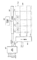
図1は本発明の一実施形態による液晶表示装置のブロック図であり、図2は本発明の実施形態による液晶表示装置の1つの画素に対する等価回路図である。
図1に示したように、本発明の一実施形態による液晶表示装置は、液晶表示板組立体(liquid crystal panel assembly)300、これに接続されたゲート駆動部400及びデータ駆動部500、データ駆動部500に接続された階調電圧生成部800、並びにこれらを制御する信号制御部600を含む。
Hereinafter, a liquid crystal display device and a liquid crystal display device driving device according to an embodiment of the display device and the display device driving device of the present invention will be described in detail with reference to the drawings.
FIG. 1 is a block diagram of a liquid crystal display device according to an embodiment of the present invention, and FIG. 2 is an equivalent circuit diagram for one pixel of the liquid crystal display device according to an embodiment of the present invention.
As shown in FIG. 1, a liquid crystal display according to an exemplary embodiment of the present invention includes a liquid
液晶表示板組立体300は、等価回路で見れば、複数の信号線G1〜Gn、D1〜Dmと、これに接続されていてほぼ行列状に配列された複数の画素PXとを含む。反面、図2に示した構造で見れば、液晶表示板組立体300は、互いに対向する下部及び上部表示板100、200と、その間に入っている液晶層3とを含む。
信号線G1〜Gn、D1〜Dmは、ゲート信号(“走査信号”とも言う)を伝達する複数のゲート線G1〜Gnと、データ信号を伝達する複数のデータ線D1〜Dmとを含む。ゲート線G1〜Gnはほぼ行方向に延在して互いにほぼ平行であり、データ線D1〜Dmはほぼ列方向に延在して互いにほぼ平行である。
In an equivalent circuit, the liquid
The signal lines G 1 to G n and D 1 to D m are a plurality of gate lines G 1 to G n that transmit gate signals (also referred to as “scanning signals”) and a plurality of data lines D 1 that transmit data signals. and a ~D m. The gate lines G 1 to G n extend in the row direction and are substantially parallel to each other, and the data lines D 1 to D m extend in the column direction and are substantially parallel to each other.
各画素PX、例えば、i番目(i=1、2、...n)ゲート線Giとj番目(j=1、2、...m)データ線Djに接続された画素PXは、信号線Gi、Djに接続されたスイッチング素子Qと、これに接続された液晶キャパシタ(liquid crystal capacitor)CLC及びストレージキャパシタ(storage capacitor)CSTとを含む。ストレージキャパシタCSTは必要に応じて省略することができる。 Each pixel PX, for example, a pixel PX connected to an i th (i = 1, 2,... N) gate line G i and a j th (j = 1, 2,... M) data line D j is , A switching element Q connected to the signal lines G i and D j , and a liquid crystal capacitor C LC and a storage capacitor C ST connected thereto. The storage capacitor CST can be omitted if necessary.
スイッチング素子Qは、下部表示板100に設けられている薄膜トランジスタなどの三端子素子であって、その制御端子はゲート線Giと接続されており、入力端子はデータ線 Dj と接続されており、出力端子は液晶キャパシタCLC及びストレージキャパシタCST と接続されている。
液晶キャパシタCLCは、下部表示板100の画素電極191と上部表示板200の共通電極270とを2つの端子とし、2つの電極191、270の間の液晶層3は誘電体として機能する。画素電極191はスイッチング素子Qと接続され、共通電極270は上部表示板200の全面に形成されていて、共通電圧Vcomの印加を受ける。図2とは異なって、共通電極270を下部表示板100に設けることもでき、この際には2つの電極191、270のうちの少なくとも1つが線状または棒状に形成することができる。
The switching element Q is a three terminal element such as a thin film transistor provided on the
In the liquid crystal capacitor C LC , the
液晶キャパシタCLCの補助的な役割を果たすストレージキャパシタCSTは、下部表示板100に設けられた別個の信号線(図示せず)と画素電極191とが絶縁体を介在して重畳して形成され、この別個の信号線には共通電圧Vcomなどの予め設定された電圧が印加される。しかし、ストレージキャパシタCSTは、画素電極191が絶縁体を媒介としてすぐ上の前段ゲート線と重畳して形成することができる。
An auxiliary role storage capacitor C ST of the liquid crystal capacitor C LC is formed separate signal line provided on the lower panel 100 (not shown) and the
一方、色表示を実現するためには、各画素PXが基本色(primary color)のうちの1つを固有に表示するように構成でき(空間分割)、また各画素PXが時間によって交互に基本色を表示するように構成する(時間分割)ことにより、これら基本色の空間的、時間的合計によって所望の色相を認識できるようにする。基本色の例としては、赤色、緑色、青色など三原色がある。 図2は、空間分割の一例として、各画素PXが画素電極191に対応する上部表示板200の領域に、基本色のうちの1つを示すカラーフィルタ230を設けたことを示している。図2とは異なって、カラーフィルタ230は下部表示板100の画素電極191上のまたは下に形成することもできる。
On the other hand, in order to realize the color display, each pixel PX can be configured to display one of the primary colors (primary color) uniquely (space division), and each pixel PX is alternately based on time. By configuring to display colors (time division), a desired hue can be recognized by the spatial and temporal sum of these basic colors. Examples of basic colors include three primary colors such as red, green, and blue. FIG. 2 shows that as an example of space division, each pixel PX is provided with a
液晶表示板組立体300の外側面には、光を偏光させる少なくとも1つの偏光子(図示せず)が付着されている。
再び図1を参照すれば、階調電圧生成部800は、画素PXの透過率と係わる2組の階調電圧集合(または基準階調電圧集合)を生成する。2組のうちの1組は、共通電圧Vcomに対して正の値(以下、“正極性階調電圧”と言う)を有し、他の1組は負の値(以下、“負極性階調電圧”と言う)を有する。
At least one polarizer (not shown) that polarizes light is attached to the outer surface of the liquid
Referring to FIG. 1 again, the
ゲート駆動部400は液晶表示板組立体300のゲート線G1〜Gnと接続され、ゲートオン電圧Vonとゲートオフ電圧Voffとの組み合わせからなるゲート信号をゲート線G1〜Gnに印加する。
データ駆動部500は液晶表示板組立体300のデータ線D1〜Dmに接続されており、階調電圧生成部800からの階調電圧を選択してこれをデータ信号としてデータ線D1〜Dmに印加する。しかし、階調電圧生成部800が全ての階調に対する電圧を全て提供することでなく、決められた数の基準階調電圧のみを提供する場合に、データ駆動部500は基準階調電圧を分圧して全体階調に対する階調電圧を生成し、この中でデータ信号を選択する。
The
信号制御部600は、ゲート駆動部400及びデータ駆動部500などを制御する。
このような駆動装置400、500、600、800は、それぞれ少なくとも1つの集積回路チップの形態で液晶表示板組立体300上に直接装着することができ、可撓性印刷回路膜(flexible printed circuit film)(図示せず)上に装着され、TCP(tape carrier package)の形態で液晶表示板組立体300に付着することもでき、別途の印刷回路基板(printed circuit board)(図示せず)上に装着することもできる。これとは異なって、これら駆動装置400、500、600、800が、信号線G1〜Gn、D1〜Dm及び薄膜トランジスタスイッチング素子Qなどと共に、液晶表示板組立体300に集積することもできる。また、駆動装置400、500、600、800は単一チップに集積することができ、この場合、これらのうちの少なくとも1つまたはこれらをなす少なくとも1つの回路素子を、単一チップの外側に構成することもできる。
The
Each of the driving
次に、このような液晶表示装置の動作について、詳細に説明する。
信号制御部600は、外部のグラフィック制御機(図示せず)から入力映像信号R、G、B及びその表示を制御する入力制御信号を受信する。入力制御信号の例としては、垂直同期信号Vsyncと水平同期信号Hsync、メインクロックMCLK、データイネーブル信号DEなどがある。
Next, the operation of such a liquid crystal display device will be described in detail.
The
信号制御部600は、入力映像信号R、G、Bと入力制御信号に基づいて入力映像信号R、G、Bを液晶表示板組立体300の動作条件に合うように適切に処理し、ゲート制御信号CONT1及びデータ制御信号CONT2などを生成した後、ゲート制御信号CONT1をゲート駆動部400に送出し、データ制御信号CONT2と処理した映像信号DATをデータ駆動部500に送出する。
The
信号制御部600のデータ処理は、所定周波数を有する入力映像信号R、G、Bを変換して、入力映像信号R、G、Bと異なる周波数、例えば2倍の周波数を有する複数の、例えば2つの出力映像信号を出力することを含む。この時、信号制御部は、入力映像信号の階調に基づいて出力映像信号のうちの1つの階調を最高階調または最低階調を有するようにする。このような信号制御部600の動作については、次に詳細に説明する。
The data processing of the
ゲート制御信号CONT1は走査開始を指示する走査開始信号STVと、ゲートオン電圧Vonの出力周期を制御する少なくとも1つのクロック信号とを含む。ゲート制御信号CONT1は、また、ゲートオン電圧Vonの持続時間を限定する出力イネーブル信号OEをさらに含むように構成できる。
データ制御信号CONT2は、1つの行の画素PXに対する映像信号の伝送開始を知らせる水平同期開始信号STHと、データ線D1〜Dmにデータ信号の印加を指示するロード信号LOAD、及びデータクロック信号HCLKを含む。データ制御信号CONT2は、また、共通電圧Vcomに対するデータ信号の電圧極性(以下、“共通電圧に対するデータ信号の電圧極性”を略して“データ信号の極性”と言う)を反転させる反転信号RVSをさらに含むように構成できる。
The gate control signal CONT1 includes a scanning start signal STV for instructing the start of scanning and at least one clock signal for controlling the output cycle of the gate-on voltage Von. The gate control signal CONT1 can also be configured to further include an output enable signal OE that limits the duration of the gate-on voltage Von.
The data control signal CONT2 includes a horizontal synchronization start signal STH for informing the start of transmission of the video signal to the pixels PX in one row, a load signal LOAD for instructing application of the data signal to the data lines D 1 to D m , and a data clock signal Includes HCLK. The data control signal CONT2 further includes an inverted signal RVS that inverts the voltage polarity of the data signal with respect to the common voltage Vcom (hereinafter, the “voltage polarity of the data signal with respect to the common voltage” is abbreviated as “the polarity of the data signal”). Can be configured to include.
信号制御部600からのデータ制御信号CONT2によって、データ駆動部500は1つの行の画素PXに対するデジタル映像信号DATを受信し、各デジタル映像信号DATに対応する階調電圧を選択することによって、デジタル映像信号DATをアナログデータ信号に変換した上で、これを該当データ線D1〜Dmに印加する。
ゲート駆動部400は、信号制御部600からのゲート制御信号CONT1によってゲートオン電圧Vonをゲート線G1〜Gnに印加し、このゲート線G1〜Gnに接続されたスイッチング素子Qを導通させる。このことにより、データ線D1〜Dmに印加されたデータ信号が導通したスイッチング素子Qを通じて該当画素PXに印加される。
In response to the data control signal CONT2 from the
The
画素PXに印加されたデータ信号の電圧と共通電圧Vcomとの差は、液晶キャパシタCLCの充電電圧、つまり、画素電圧として現れる。液晶分子は画素電圧の大きさによってその配列を異にし、そのために液晶層3を通過する光の偏光が変化する。このような偏光の変化は表示板組立体300に付着された偏光子によって光の透過率変化として現れる。
1水平周期(“1H”とも記し、水平同期信号Hsync及びデータイネーブル信号DEの一周期と同一である)を単位としてこのような過程を繰り返すことによって、全てのゲート線G1〜Gnに対して順にゲートオン電圧Vonを印加し、全ての画素PXにデータ信号を印加して1フレームの映像を表示する。
The difference between the voltage of the data signal applied to the pixel PX and the common voltage Vcom appears as the charging voltage of the liquid crystal capacitor CLC , that is, the pixel voltage. The arrangement of the liquid crystal molecules differs depending on the magnitude of the pixel voltage, and the polarization of light passing through the
By repeating such a process in units of one horizontal cycle (also referred to as “1H”, which is the same as one cycle of the horizontal synchronization signal Hsync and the data enable signal DE), all the gate lines G 1 to G n are repeated. Then, a gate-on voltage Von is sequentially applied, and a data signal is applied to all the pixels PX to display one frame of video.
1フレームが終了した後、次のフレームが始まり、各画素PXに印加されるデータ信号の極性が直前のフレームでの極性と反対になるように、データ駆動部500に印加される反転信号RVSの状態が制御される(“フレーム反転”)。この時、1フレーム内でも反転信号RVSの特性によって1つのデータ線を通じて流れるデータ信号の極性を変えることができ(例:行反転、点反転)、1つの画素行に印加されるデータ信号の極性を互いに異なるように構成することもできる(例:列反転、点反転)。
After the end of one frame, the next frame starts and the inverted signal RVS applied to the
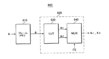
次に、図3を参照して、本発明の一実施形態による液晶表示装置の信号制御部600でのデータ信号の処理について説明する。
信号制御部600は、フレームメモリ610と、これに接続されている映像信号補正部620とを含む。
フレームメモリ610は、入力される映像信号をフレーム単位で記憶し、この際のフレームメモリ610に記憶されている映像信号を入力映像信号grとして表記する。
Next, with reference to FIG. 3, processing of data signals in the
The
The
映像信号補正部620は、フレームメモリ610に記憶されている入力映像信号grを順に受信して、入力映像信号grを複数の出力映像信号、例えば、第1及び第2出力映像信号gr1、gr2に変換して順に出力する。具体的に説明すれば、映像信号補正部620は入力映像信号grを一回ずつ読み取って第1出力映像信号gr1に変換し順に出力した上で、入力映像信号grを再び1回ずつ読み取って第2出力映像信号gr2に変換し順に出力する。これにより、データ駆動部500は全ての画素に対して第1出力映像信号gr1に該当するデータ信号をデータ線D1〜Dmに印加した後、第2出力映像信号gr2に該当するデータ信号をデータ線D1〜Dmに印加する。以下では、第1及び第2出力映像信号gr1、gr2が出力される期間、及び第1及び第2出力映像信号gr1、gr2に該当するデータ信号が印加される期間のそれぞれをフィールドと言う。この2つのフィールドの期間は各々1/2Hである。このような映像信号補正部620については次に詳細に説明する。
一方、フレームメモリ610に記憶されている入力映像信号grを2回ずつ読み取るため、フレームメモリ610の読み取り周波数(read frequency)(または出力周波数)は、書き込み周波数(write frequency)(または入力周波数)の2倍である。これによって、フレームメモリ610の入力フレーム周波数が60Hzであれば、映像信号補正部620の出力フィールド周波数及びデータ信号の印加周波数も120Hzになる。
Meanwhile, to read the input video signal g r stored in the
2つの出力映像信号gr1、gr2は、第1及び第2出力映像信号 gr1、gr2による画素の光量の合計が補正前の入力映像信号grによる光量と同一である。ここで、光量とは、輝度とその輝度を維持する時間をかけたものと同一である。
従って、入力映像信号grに対応する輝度をT(gr)とし、第1出力映像信号gr1に対応する輝度をT(gr1)とし、第2出力映像信号gr2に対応する輝度をT(gr2)とすれば、
(数式1)
2T(gr)=T(gr1)+T(gr2)が成立する。
Two output video signal g r1, g r2, the total amount of pixels by the first and second output image signals g r1, g r2 is the same as the light amount by the input image signal g r before correction. Here, the light amount is the same as the luminance and the time over which the luminance is maintained.
Thus, a luminance corresponding to the input video signal g r and T (g r), the luminance corresponding to the first output image signal g r1 and T (g r1), the luminance corresponding to the second output image signal g r2 T (g r2 )
(Formula 1)
2T (g r ) = T (g r1 ) + T (g r2 ) is established.
また、2つの出力映像信号gr1、gr2の階調Pr1、Pr2のうちの1つは、他の1つより大きいか同一である。
つまり、Pr1≧Pr2またはPr1≦Pr2である。
この時、2つの出力映像信号gr1、gr2の階調Pr1、Pr2のうちの大きい階調を有する出力映像信号を上位出力映像信号とし、小さい階調を有する出力映像信号を下位出力映像信号とし、上位出力映像信号を先に出力するように構成でき、またはその反対にすることもできる。この時、上位出力映像信号が出力されるフィールドは上位フィールド、下位出力映像データが出力されるフィールドは下位フィールドとする。
Also, one of the gradations P r1 and P r2 of the two output video signals g r1 and g r2 is greater than or equal to the other one.
That is, P r1 ≧ P r2 or P r1 ≦ P r2 .
At this time, an output video signal having a larger gradation of the gradations P r1 and P r2 of the two output video signals g r1 and g r2 is used as an upper output video signal, and an output video signal having a smaller gradation is output as a lower order. The video signal can be configured to output the higher-level output video signal first, or vice versa. At this time, the field from which the higher output video signal is output is the upper field, and the field from which the lower output video data is output is the lower field.
下位出力映像信号による光量は、上位出力映像信号による光量の約50%を越えないことが好ましく、下位出力映像信号の階調は0、つまり、ブラック階調またはそれに近くすることでインパルシブ駆動の効果を与えることができる。
上記の条件を満たしながらインパルシブ駆動の効果を与える上位出力映像信号と下位出力映像信号を得るための一実施形態について詳細に説明する。
The amount of light by the lower output video signal preferably does not exceed about 50% of the amount of light by the upper output video signal, and the gradation of the lower output video signal is 0, that is, the black gradation or close to it, the effect of impulsive driving Can be given.
An embodiment for obtaining an upper output video signal and a lower output video signal that give the effect of impulsive driving while satisfying the above conditions will be described in detail.
本実施形態において、Pr1≧Pr2の場合、Pr1の階調を有する第1出力映像信号gr1を上位出力映像信号とし、Pr2の階調を有する第2出力映像信号gr2を下位出力映像信号とし、下位出力映像信号より先に上位出力映像信号を出力するものと仮定する。これとは反対の場合を適用できることは当然である。
フレームメモリ610に記憶された入力映像信号grが8ビットである時、入力映像信号grの階調Prは0〜255であり、この階調Prを有する入力映像信号grの輝度[T(gr)]は次のような関係を有する。
In this embodiment, when P r1 ≧ P r2 , the first output video signal g r1 having the gradation of P r1 is set as the upper output video signal, and the second output video signal g r2 having the gradation of P r2 is set as the lower order. Assume that an output video signal is output, and an upper output video signal is output before a lower output video signal. Of course, the opposite case is applicable.
When the input video signal g r stored in the
T(gr)=α(Pr/255)γ
γ=2.4である時、入力映像信号grの階調Prが192であれば、最大階調である255の半分程度の輝度を示す。従って、次のように上位出力映像信号gr1の階調Pr1と下位出力映像信号gr2の階調Pr2とを定める。
(1)0≦Pr≦192であれば、Pr1=(255/192)×Pr、Pr2=0
(2)193≦Pr≦255であれば、Pr1=255、Pr2=T-1[2T(Pr)−T(255)]
つまり、入力映像信号grの階調Prが(1)の区間に含まれる場合、上位出力映像信号gr1の階調Pr1は入力映像信号grの階調Prに従って最大255まで決められ、下位出力映像信号gr2の階調Pr2は0である。
T (g r ) = α (P r / 255) γ
When gamma = 2.4, if the gradation P r of the input image signal g r is 192, indicating the order of half the luminance of 255 is the maximum gradation. Thus, defining the gradation P r2 of gradation P r1 and lower output image signal g r2 of upper output image signal g r1 as follows.
(1) If 0 ≦ P r ≦ 192, then P r1 = (255/192) × P r , P r2 = 0
(2) If 193 ≦ P r ≦ 255, then P r1 = 255, P r2 = T −1 [2T (P r ) −T (255)]
That is, when the gradation P r of the input image signal g r is included in the section of (1) the gradation P r1 of the upper output image signal g r1 is determined up to 255 as the gray P r of the input image signal g r is, the gradation P r2 of the lower output image signal g r2 is zero.
入力映像信号grの階調Prが(2)の区間に含まれる場合、上位出力映像信号gr1の階調Pr1は最大階調である255を有するようになり、下位出力映像信号gr2の階調Pr2は(数式1)を満たす値になる。入力映像信号grの階調Prが255である時、上位出力映像信号gr1の階調Pr1と下位出力映像信号gr2の階調Pr1は全て255となる。
入力映像信号grの階調Prが128、192、224及び255である時、(1)と(2)によって得られた各上位出力映像信号gr1に対応するデータ信号と、下位出力映像信号gr2に対応するデータ信号を図4に示す。
When the gradation P r of the input image signal g r is included in the section (2), the gradation P r1 of the upper output image signal g r1 becomes to have a 255 a maximum gradation, lower output image signal g gradation P r2 of r2 is a value that satisfies (equation 1). When the gradation P r of the input image signal g r is 255, the gradation P r1 of gradation P r1 and lower output image signal g r2 of upper output image signal g r1 are all 255.
When the gradation P r of the input image signal g r is 128,192,224 and 255, a data signal corresponding to each upper output image signal g r1 obtained by (1) and (2), lower output image A data signal corresponding to the signal gr2 is shown in FIG.
図4に示したように、各フィールドの間に該当出力映像信号gr1、gr2に対応するデータ信号を印加する時、入力映像信号grの階調Prが192以下である場合、上位出力映像信号gr1の階調Pr1は最大階調である255以下の範囲から選択される。この時、上位出力映像信号gr1の階調Pr1は入力映像信号grの階調Prより大きい階調となる。第1及び第2フィールドの間に各出力映像信号gr1、gr2に対応するデータ信号を該当画素に印加するので、上位または下位出力映像信号gr1、gr2に対応するデータ信号が印加される時間を2つのフィールドに分けず、入力映像信号grに対応するデータ信号を該当画素に印加する時より約1/2に減少する。従って、入力映像信号grに対応するデータ信号よりさらに大きいデータ信号を印加してこそ入力映像データgrによる光量とほとんど同一の光量を得ることができる。こういう場合、つまり、入力映像信号grの階調Prが192を越えない場合、上位出力映像信号gr1に対応するデータ信号だけでほとんど入力映像信号grによる光量を得ることができるので、下位出力映像信号gr2の階調Pr2を0としてインパルシブ駆動の効果を得ることができる。 As shown in FIG. 4, when applying a data signal corresponding to the relevant output image signal g r1, g r2 during each field, when the gray P r of the input image signal g r is 192 or less, the upper gradation P r1 of the output video signal g r1 is selected from 255 the following range is a maximum gradation. At this time, the gradation P r1 of the upper output image signal g r1 becomes gradation P r is larger than the gradation of the input image signal g r. Since the data signals corresponding to the output video signals g r1 and g r2 are applied to the corresponding pixels between the first and second fields, the data signals corresponding to the upper or lower output video signals g r1 and g r2 are applied. without dividing the amount of time into two fields, reducing the data signal corresponding to the input video signal g r to about 1/2 than when applied to the corresponding pixel. Therefore, it is possible to obtain almost the same light quantity and the input image signal g Only by applying a larger data signal from the data signal corresponding to r amount by the input image data g r. These cases, i.e., when the gradation P r of the input image signal g r does not exceed 192, it is possible to almost give a light amount by the input image signal g r only data signal corresponding to the upper output image signal g r1, gradation P r2 of the lower output image signal g r2 has the advantages of impulsive driving as 0.
しかし、入力映像信号grの階調Prが192を越える場合、下位出力映像信号gr2の階調Pr2を0とすれば、上位出力映像信号gr1の階調Pr2を最大階調である255に決めても、入力映像信号grのような光量が得られない。つまり、輝度損失が発生する。従って、下位出力映像信号gr2の階調Pr2を0より大きい値に決めて不足した光量を下位出力映像信号gr2による光量で補償する。この場合、たとえインパルシブ駆動効果を出す下位出力映像信号gr2の階調Pr2が0ではないが、低い階調、例えば、0に近い階調を有しているので、ある程度インパルシブ駆動の効果を得るようになる。
However, when the gray P r of the input image signal g r exceeds 192, if the gradation P r2 of the lower output
このように全部で256個の入力映像信号grの階調Prのうちの約3/4に相当する0〜192の範囲の中で1つの階調を有する入力映像信号grに対する下位出力映像信号gr2の階調Pr2が0でインパルシブ駆動を行い、残り1/4範囲に属する階調のうちの1つを有する入力映像信号grに対する下位出力映像信号gr2が0に近い低い階調を有するようになるので、多くの光量の損失なしに、つまり、輝度を大きく向上させながらインパルシブ駆動の効果が得られる。 Lower output the input video signal g r having such a single tone in the range of equivalent 0-192 to approximately 3/4 of the gradation P r of a total of 256 input video signals g r gradation P r2 of the video signal g r2 performs impulsive driving at 0, low near the lower output image signal g r2 is 0 for the input video signal g r with one of the gradations belonging to the remaining 1/4 range Since it has gradation, the effect of impulsive driving can be obtained without much loss of light quantity, that is, while greatly improving the luminance.
このような方式で得られた入力映像信号grに対する2つの出力映像信号gr1、gr2をデータ駆動部500に伝達する信号制御部600の動作について、再び図4を参照して説明する。
既に説明したように、信号制御部600は、フレームメモリ610と映像信号補正部620とを含む。映像信号補正部620は、フレームメモリ610に接続されたルックアップテーブル630、及びルックアップテーブル630に接続されており、フィールド選択信号FSを受信するマルチプレクサー640を含む。この時、フィールド選択信号FSは多様な方式で定めることができるが、単純にフィールドの奇偶で決定することができ、カウンターなどを用いて決定することもできる。また、このフィールド選択信号FSは、信号制御部600の内部で生成できるが、外部から提供される信号を用いることもできる。
The operation of the
As already described, the
既にフレームメモリ610については前述したため、これに対する説明は省略する。
映像信号補正部620のルックアップテーブル630には、上位出力映像信号gr1と下位出力映像信号gr2が入力映像信号grの関数で記憶されている。従って、ルックアップテーブル630は入力映像信号grに応答して、これに対応する上位及び下位出力映像信号gr1、gr2をマルチプレクサー640に送出する。
Since the
The look-up table 630 of the video
マルチプレクサー640は、フィールド選択信号FSの値によってルックアップテーブル630からの上位及び下位出力映像信号gr1、gr2のうちの1つを選択し、順にデータ駆動部500に出力する。
このようにデータ駆動部500を経てデータ線D1〜Dmを通じて画素に印加される上位出力映像信号と下位出力映像信号gr1、gr2に対応するデータ信号は、図5に示したような反転形態を有する。図5の(a)は第1フィールドに上位出力映像信号に対応するデータ信号が印加される場合の反転形態を示したものであり、図5の(b)は第2フィールドに上位出力映像信号に対応するデータ信号が印加される場合の反転形態を示したものである。
The
The data signals corresponding to the upper output video signal and the lower output video signals g r1 and g r2 applied to the pixels through the data lines D 1 to D m through the
上位出力映像信号に対応するデータ信号の電圧極性は、隣接した直前のフィールドの極性と同一であれば、映像に影響を与える上位出力映像信号による画素の充電速度が減少する。
また、フレームごとに上位出力映像信号に対応するデータ信号の電圧極性が反転し、下位出力映像信号に対応するデータ信号の電圧極性が反転することにより、画素電圧の平均が“+”極性や“−”極性のうちのいずれかに片寄ることがない。
If the voltage polarity of the data signal corresponding to the upper output video signal is the same as the polarity of the immediately preceding adjacent field, the pixel charging rate by the upper output video signal affecting the video is reduced.
In addition, the voltage polarity of the data signal corresponding to the higher-order output video signal is inverted for each frame, and the voltage polarity of the data signal corresponding to the lower-order output video signal is inverted, so that the average pixel voltage becomes “+” polarity or “ -"Never deviate from any of the polarities.
従って、第1フィールドに上位出力映像信号が印加された場合、図5の(a)に示したように、2つのフィールドに印加されるデータ信号の極性は互いに反対であり、隣接したフレーム間の極性も反対であり、各画素の極性は2つのフィールドごとに反転する。
第2フィールドに上位出力映像信号が印加された場合、図5の(b)に示したように、1フレーム内の2つのフィールドに印加されるデータ信号の電圧極性は同一であり、隣接したフレーム間の極性は反対であり、各画素の極性は2つのフィールドごとに反転する。
Therefore, when the upper output video signal is applied to the first field, the polarities of the data signals applied to the two fields are opposite to each other as shown in FIG. The polarity is also opposite, and the polarity of each pixel is inverted every two fields.
When the upper output video signal is applied to the second field, the voltage polarity of the data signal applied to the two fields in one frame is the same as shown in FIG. The polarity between them is opposite, and the polarity of each pixel is inverted every two fields.
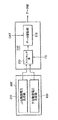
次に、前述した図1及び図3の他にも図6A〜図7Bを参照して、本発明の他の実施形態による液晶表示装置について説明する。本実施形態による液晶表示装置は階調電圧生成部800'とデータ駆動部500'を除いては、図1に示した液晶表示装置の構造及び動作と同一であるので、階調電圧生成部800'とデータ駆動部500'の構造及び動作についてのみ詳細に説明する。
Next, in addition to FIGS. 1 and 3 described above, a liquid crystal display device according to another embodiment of the present invention will be described with reference to FIGS. 6A to 7B. The liquid crystal display device according to the present embodiment has the same structure and operation as the liquid crystal display device shown in FIG. 1 except for the
図6A及び図6B各々は本発明の他の実施形態による階調電圧生成部とデータ駆動部のブロック図である。また、図7Aは本発明の他の実施形態によって上位階調を有する上位出力映像信号に対する階調電圧を示したグラフであり、図7Bは本発明の他の実施形態によって下位階調を有する下位出力映像信号に対する階調電圧を示したグラフである。
図6Aに示したように、本実施形態による階調電圧生成部800'は上位階調電圧生成器810と下位階調電圧生成器820とを含み、データ駆動部500'は、フィールド選択信号FSによってこれら2つの階調電圧生成器810、820のうちの1つを選択するスイッチング部850と、スイッチング部850に接続されたデータ駆動回路510とを含んでいる。データ駆動回路510は、図1に示したデータ駆動部500と同じ構造であって同様に動作するので、これに対する詳細な説明は省略する。
6A and 6B are block diagrams of a gray voltage generator and a data driver according to another embodiment of the present invention. FIG. 7A is a graph illustrating a gray scale voltage for an upper output video signal having higher gray levels according to another embodiment of the present invention, and FIG. 7B is a lower graph having lower gray levels according to another embodiment of the present invention. 6 is a graph showing a gradation voltage with respect to an output video signal.
As shown in FIG. 6A, the
図6Bに示した液晶表示装置においては、図6Aに示したスイッチング素子850がデータ駆動部500の外部に装着される別個の装置と設計されていることを除けば、他の構造や動作は図6Aに示した液晶表示装置と同一である。
スイッチング部850は、フィールド選択信号FSの状態によってスイッチング状態が変わるアナログスイッチで構成することができる。
In the liquid crystal display device shown in FIG. 6B, other structures and operations are not shown except that the switching
The
上位及び下位階調電圧生成器810、820は各々複数の電圧を生成する抵抗列を含んでいる。
図3に基づいて前述したように、入力映像信号grの関数で上位出力映像信号gr1と下位出力映像信号gr2が信号制御部600のルックアップテーブル630に記憶されている時、これら映像信号gr、gr1、gr2それぞれの階調Pr、Pr1、Pr2に対する透過率曲線(以下、“ガンマ曲線”と言う)を、図7に示したように、各々“T”、“T1”及び“T2”とする。
Each of the upper and lower
As described above with reference to FIG. 3, when the upper output image signal g r1 and lower output image signal g r2 are stored in a look-up table 630 of the
この時、上位階調電圧生成器810から出力される複数の階調電圧は、図7Aに示したように、上位出力映像信号gr1に対するガンマ曲線T1に基づいて決められた階調電圧集合V0、V1、V2、V3、...となり、下位階調電圧生成器820から出力される複数の階調電圧は、図7Bに示したように、下位出力映像信号gr2に対するガンマ曲線T2に基づいて決められた階調電圧集合V0'、V1'、V2'、V3'、...となる。
At this time, the plurality of gradation voltages output from the upper
このように、上位階調電圧生成器810と下位階調電圧生成器820から出力される階調電圧集合を決定する時、これら2つの階調電圧生成器810、820において該当する階調電圧を選択するデータ駆動部500'、500の動作について説明する。
まず、入力映像信号grに対応する上位/下位出力映像信号gr1、gr2が映像信号DATとして順にデータ駆動部500'、500に印加され、信号制御部600のマルチプレクサー640に印加されるフィールド選択信号FSもスイッチング部850に印加される。フィールド選択信号FSの状態によって、スイッチング部850は上位階調電圧生成器810または下位階調電圧生成器820からの階調電圧集合V0'、V1'、V2'、V3'、...またはV0、V1、V2、V3、...のうちの1つの階調電圧集合を選択して、データ駆動回路510(またはデータ駆動部500)に印加する。
As described above, when determining a set of grayscale voltages output from the upper
First, the upper / lower output image signal g r1, g r2 is the
データ駆動回路510(またはデータ駆動部500)は、印加された階調電圧集合の中で印加されたデジタル映像信号DATに対応する電圧を選択した後、データ信号として出力する。
このように、上位出力映像信号gr1と下位出力映像信号gr2各々に対応する階調電圧生成器が設けられているので、各上位出力映像信号gr1と下位出力映像信号gr2に対する全ての階調を表現する。これについてさらに詳細に説明する。
The data driving circuit 510 (or the data driving unit 500) selects a voltage corresponding to the applied digital video signal DAT from the applied gradation voltage set, and then outputs it as a data signal.
Thus, since the upper output image signal g r1 and lower output image signal g r2 gray voltage generator corresponding to each is provided, all for each upper output image signal g r1 and lower output image signal g r2 Express gradation. This will be described in more detail.
例えば、表現可能な階調の数が全部で256個である場合、階調電圧生成部が1つの階調電圧生成器だけで構成されているならば、この時出力される正極性及び負極性の階調電圧の数は各々256個である。この時、各256個の入力階調に対する上位出力映像信号gr1の透過率の個数と下位出力映像信号gr2の透過率の個数も、各々256個である。上位出力映像信号gr1の透過率と下位出力映像信号gr2の透過率の中で互いに同一の値を有する透過率が存在しないと仮定する場合、256個の入力階調に対応する全透過率の個数は、上位出力映像信号gr1の透過率個数と下位出力映像信号gr2の透過率個数を全て合せた512個である。つまり、上位出力映像信号gr1と下位出力映像信号gr2に対応する透過率を全て表現するためには、全て512個の階調電圧(正極性の階調電圧または負極性の階調電圧だけ考慮する時)が必要となる。 For example, when the number of gradations that can be expressed is 256 in total, if the gradation voltage generator is composed of only one gradation voltage generator, the positive polarity and the negative polarity that are output at this time. The number of gradation voltages of each is 256. At this time, the number of transmittances of the higher-order output video signal gr1 and the number of transmittances of the lower-order output video signal gr2 for each of the 256 input gradations are 256 each. When it is assumed that there is no transmittance having the same value in the transmittance of the upper output video signal gr1 and the transmittance of the lower output video signal gr2 , the total transmittance corresponding to 256 input gradations. Is 512, which is the sum of the number of transmittances of the upper output video signal gr1 and the number of transmittances of the lower output video signal gr2 . In other words, in order to express all the transmissivities corresponding to the higher-order output video signal gr1 and the lower-order output video signal gr2 , all 512 gradation voltages (only positive gradation voltage or negative gradation voltage are used). When considering).
しかし、1つの階調電圧生成器だけを利用する場合、各極性に対して256個の階調電圧しか出力できないので、残り256個の透過率に対する階調電圧を生成できないという問題が生じ、各上位出力映像信号gr1と下位出力映像信号gr2に対する正確な階調表現が行われない。
実質的に同一の透過率を有する上位出力映像信号gr1と下位出力映像信号gr2が一部存在するが、上位出力映像信号gr1と下位出力映像信号gr2のガンマ曲線T1、T2の傾きが互いに相異していて、区間によっても透過率の変化が一定でないため、出力映像信号gr1、gr2に対する全透過率の個数は256個をはるかに超える。
However, when only one gradation voltage generator is used, since only 256 gradation voltages can be output for each polarity, there arises a problem that gradation voltages for the remaining 256 transmittances cannot be generated. Accurate gradation representation is not performed for the upper output video signal gr1 and the lower output video signal gr2 .
Although upper output image signal g r1 and lower output image signal g r2 having substantially the same transmittance exists some, the slope of the gamma curve T1, T2 of the upper output image signal g r1 and lower output image signal g r2 Are different from each other, and the change in transmittance is not constant depending on the section, so that the total number of transmittances for the output video signals g r1 and g r2 far exceeds 256.
既に説明したように、1つの階調電圧生成器だけを利用する場合、上位出力映像信号gr1と下位出力映像信号gr2に対する全ての階調表現が行われない。
しかし、本実施形態においては、上位出力映像信号gr1と下位出力映像信号gr2各々に対応する階調電圧生成器810、820から階調電圧集合が生成されるので、上位出力映像信号gr1と下位出力映像信号gr2に対する全ての階調表現が可能である。また、1つの入力映像信号はデジタル信号処理を通じて該当する階調を有する2つの出力映像信号に変換されるので、小数点のようにデジタル的に表現できない信号値によって発生する量子化エラー(quantization error)も減少する。
As already described, when only one gradation voltage generator is used, not all gradation representations for the upper output video signal gr1 and the lower output video signal gr2 are performed.
However, in the present embodiment, since the gray voltage set is generated from the upper output image signal g r1 and lower output image signal g r2
このように、第1実施形態によって1つの階調電圧生成器を含む場合と第2実施形態によって2つの階調電圧生成器を利用する場合、各々上位出力映像信号と下位出力映像信号に対するガンマ曲線を図8を参照して比較してみる。
図8は本発明の第1及び第2実施形態による上位出力映像信号と下位出力映像信号に対するガンマ曲線を示したグラフである。
As described above, when one gradation voltage generator is included according to the first embodiment and when two gradation voltage generators are used according to the second embodiment, the gamma curves for the upper output video signal and the lower output video signal, respectively. Are compared with reference to FIG.
FIG. 8 is a graph showing gamma curves for the upper output video signal and the lower output video signal according to the first and second embodiments of the present invention.
次に、図8を参照して、第1実施形態による階調電圧に対する透過率曲線と第2実施形態による階調電圧に対する透過率曲線を比較してみる。
図8に示すように、1つの階調電圧生成器を利用する場合、上位出力映像信号のガンマ曲線U1と下位出力映像信号に対するガンマ曲線L1を見てみると、曲線U1、L1の傾きが徐々に変化するのではなく、“A”部分でのように突然大幅に傾きが変わる区間が発生し、これによる突然の透過率変化は画質の悪化を招く。
Next, referring to FIG. 8, the transmittance curve for the grayscale voltage according to the first embodiment is compared with the transmittance curve for the grayscale voltage according to the second embodiment.
As shown in FIG. 8, when one gradation voltage generator is used, when looking at the gamma curve U1 of the upper output video signal and the gamma curve L1 of the lower output video signal, the slopes of the curves U1 and L1 gradually increase. Instead, a section where the slope suddenly changes significantly as in the “A” portion is generated, and a sudden change in transmittance due to this causes a deterioration in image quality.
これに比べて、2つの階調電圧生成器を利用する場合、上位出力映像信号のガンマ曲線U2と下位出力映像信号に対するガンマ曲線L2は突然に傾きが大幅に変わる区間がなく、ガンマ曲線の歪曲(distortion)なしで全区間でほとんど一定の傾きを有することが見られる。これによって、階調変化によって順次に透過率も変わるようになって、画質が良くなる。 In contrast, when two grayscale voltage generators are used, the gamma curve U2 of the higher-order output video signal and the gamma curve L2 of the lower-order output video signal do not have a section where the slope changes suddenly and the gamma curve is distorted. It can be seen that there is almost constant slope over the whole interval without (distortion). As a result, the transmittance is also changed sequentially according to the gradation change, and the image quality is improved.
本実施形態においては、インパルシブ実現などのために、互いに異なる階調の入力映像信号に対して同一の階調を有する上位出力映像信号と下位出力映像信号が複数個存在し、これによって、入力映像信号に対して各々上位出力映像信号と下位出力映像信号が一対一に対応せず、各入力映像信号に合致するように正確な値への抵抗値調整が困難であり、また、抵抗列の抵抗値を調整した後、液晶表示装置の特性などを考慮して決められた上位/下位出力映像信号の階調を調整するために、ルックアップテーブルを含む映像信号補正部を利用している。しかし、別途のルックアップテーブルなどを利用せず、直ちに入力映像信号とスイッチング部の動作によって該当する階調電圧生成器を選択し、1つの階調電圧を選択するように構成することも可能である。 In the present embodiment, in order to achieve impulsive, etc., there are a plurality of higher-order output video signals and lower-order output video signals having the same gradation with respect to input video signals of different gradations. The upper output video signal and the lower output video signal do not correspond one-to-one with the signal, and it is difficult to adjust the resistance value to an accurate value so as to match each input video signal. After adjusting the value, a video signal correction unit including a lookup table is used to adjust the gradation of the upper / lower output video signal determined in consideration of the characteristics of the liquid crystal display device. However, instead of using a separate look-up table or the like, it is also possible to select a single grayscale voltage by immediately selecting the corresponding grayscale voltage generator by the operation of the input video signal and the switching unit. is there.
また、本実施形態は、1つの入力映像信号に基づいて上位/下位出力映像信号に変換する時、上位または下位出力映像信号の階調を調整してインパルシブ実現が可能な液晶表示装置だけでなく、1つの入力映像信号に基づいて上位/下位出力映像信号のような複数の出力映像信号に変換して映像を表示する全ての表示装置に適用することができる。
以上、本発明の好ましい実施形態について詳細に説明したが、本発明の権利範囲はこれに限定されるわけではなく、添付した請求範囲で定義している本発明の基本概念を利用した当業者の種々の変形及び改良形態も本発明の権利範囲に属するものである。
In addition, the present embodiment is not limited to a liquid crystal display device that can be implemented impulsively by adjusting the gradation of the upper or lower output video signal when converting to the upper / lower output video signal based on one input video signal. The present invention can be applied to all display devices that display video by converting into a plurality of output video signals such as upper / lower output video signals based on one input video signal.
The preferred embodiments of the present invention have been described in detail above, but the scope of the present invention is not limited thereto, and those skilled in the art using the basic concept of the present invention defined in the appended claims. Various modifications and improvements are also within the scope of the present invention.
3 液晶層
100、200 表示板
191 画素電極
230 カラーフィルタ
270 共通電極
300 液晶表示板組立体
400 ゲート駆動部
500、500’ データ駆動部
510 データ駆動回路
600 信号制御部
610 フレームメモリ
620 映像信号補正部
630 ルックアップテーブル
640 マルチプレクサー
800、800’ 階調電圧生成部
810 上位階調電圧生成器
820 下位階調電圧生成器
850 スイッチング部
G1〜Gn ゲート線
D1〜Dm データ線
PX 画素
Q スイッチング素子
CLC 液晶キャパシタ
CST ストレージキャパシタ
R、G、B 入力映像信号
CONT1 ゲート制御信号
CONT2 データ制御信号
DAT 映像信号
Von ゲートオン電圧
Voff ゲートオフ電圧
OE 出力イネーブル信号
STV 走査開始信号
STH 水平同期開始信号
LOAD ロード信号
HCLK データクロック信号
Vcom 共通電圧
RVS 反転信号
FS フィールド選択信号
gr 入力映像信号
gr1、gr2 出力映像信号
Pr、Pr1、Pr2 階調
3
Claims (20)
第1周波数の入力映像信号を第2周波数の複数の出力映像信号に変換して出力する信号制御部と、
前記複数の出力映像信号に各々対応する複数の階調電圧集合を生成する階調電圧生成部と、
前記複数の出力映像信号に対応するそれぞれのデータ信号を1つの階調電圧集合の中で選択して前記画素に印加するデータ駆動部と、
を含む表示装置。 A plurality of pixels arranged in a matrix;
A signal control unit that converts an input video signal of a first frequency into a plurality of output video signals of a second frequency and outputs the same;
A gray voltage generator that generates a plurality of gray voltage sets respectively corresponding to the plurality of output video signals;
A data driver for selecting each of the data signals corresponding to the plurality of output video signals from one grayscale voltage set and applying the selected data signal to the pixel;
Display device.
前記複数の出力映像信号による光量の合計は前記入力映像信号による光量と同一である、請求項1に記載の表示装置。 The luminance of the pixel is determined according to the data signal,
The display device according to claim 1, wherein a total light amount by the plurality of output video signals is the same as a light amount by the input video signals.
前記第1出力映像信号の階調は前記第2出力映像信号の階調より大きいか同じである、 請求項1または4に記載の表示装置。 The plurality of output video signals include a first output video signal and a second output video signal;
The display device according to claim 1, wherein a gradation of the first output video signal is greater than or equal to a gradation of the second output video signal.
前記入力映像信号が記憶されているフレームメモリと、
前記入力映像信号の関数で前記複数の出力映像信号が記憶されており、前記フレームメモリからの入力映像信号に該当する複数の出力映像信号を送出するルックアップテーブルと、
制御信号によって前記ルックアップテーブルからの複数の出力映像データのうちの1つを選択して送出するマルチプレクサーと、
を含む、請求項1に記載の表示装置。 The signal controller is
A frame memory in which the input video signal is stored;
A plurality of output video signals stored as a function of the input video signal, and a lookup table for sending a plurality of output video signals corresponding to the input video signal from the frame memory;
A multiplexer that selects and transmits one of a plurality of output video data from the lookup table according to a control signal;
The display device according to claim 1, comprising:
第1周波数の入力映像信号を第2周波数の複数の出力映像信号に変換して出力する信号制御部と、
前記複数の出力映像信号に各々対応する複数の階調電圧集合を生成する階調電圧生成部と、
前記複数の出力映像信号に対応するそれぞれのデータ信号を1つの階調電圧集合の中で選択して前記画素に印加するデータ駆動部と、
を含む表示装置の駆動装置。 A device for driving a display device including a plurality of pixels,
A signal control unit that converts an input video signal of a first frequency into a plurality of output video signals of a second frequency and outputs the same;
A gray voltage generator that generates a plurality of gray voltage sets respectively corresponding to the plurality of output video signals;
A data driver for selecting each of the data signals corresponding to the plurality of output video signals from one grayscale voltage set and applying the selected data signal to the pixel;
A drive device for a display device, comprising:
前記複数の出力映像信号による光量の合計は前記入力映像信号による光量と同一である、請求項9に記載の表示装置の駆動装置。 The luminance of the pixel is determined according to the data signal,
The drive device of the display device according to claim 9, wherein a total light amount by the plurality of output video signals is the same as a light amount by the input video signals.
前記第1出力映像信号の階調は前記第2出力映像信号の階調より大きいか同じである、請求項9または12に記載の表示装置の駆動装置。 The plurality of output video signals include a first output video signal and a second output video signal,
The driving device of the display device according to claim 9 or 12, wherein a gradation of the first output video signal is greater than or equal to a gradation of the second output video signal.
前記入力映像信号が記憶されているフレームメモリと、
前記フレームメモリからの前記入力映像信号に基づいて前記第1出力映像信号と前記第2出力映像信号とを送出する映像信号補正部と、
を含む、請求項13に記載の表示装置の駆動装置。 The signal controller is
A frame memory in which the input video signal is stored;
A video signal correction unit for sending the first output video signal and the second output video signal based on the input video signal from the frame memory;
The drive device for a display device according to claim 13, comprising:
前記入力映像信号の関数で前記第1出力映像信号と前記第2出力映像信号が記憶されており、前記フレームメモリからの入力映像信号に該当する前記第1出力映像データと前記第2出力映像データを送出するルックアップテーブルと、
制御信号によって前記ルックアップテーブルからの第1出力映像データと第2出力映像データのうちの1つを選択して送出するマルチプレクサーと
を含む、請求項17に記載の表示装置の駆動装置。 The video signal correction unit is
The first output video signal and the second output video signal are stored as a function of the input video signal, and the first output video data and the second output video data correspond to the input video signal from the frame memory. A lookup table that sends
The display device driving device according to claim 17, further comprising: a multiplexer that selects and transmits one of the first output video data and the second output video data from the lookup table according to a control signal.
Applications Claiming Priority (1)
| Application Number | Priority Date | Filing Date | Title |
|---|---|---|---|
| KR1020050049915A KR20060128450A (en) | 2005-06-10 | 2005-06-10 | Display device and driving apparatus thereof |
Publications (2)
| Publication Number | Publication Date |
|---|---|
| JP2006350342A true JP2006350342A (en) | 2006-12-28 |
| JP2006350342A5 JP2006350342A5 (en) | 2009-06-18 |
Family
ID=37510100
Family Applications (1)
| Application Number | Title | Priority Date | Filing Date |
|---|---|---|---|
| JP2006162120A Withdrawn JP2006350342A (en) | 2005-06-10 | 2006-06-12 | Display device and apparatus for driving display device |
Country Status (5)
| Country | Link |
|---|---|
| US (1) | US20060279786A1 (en) |
| JP (1) | JP2006350342A (en) |
| KR (1) | KR20060128450A (en) |
| CN (1) | CN1877685B (en) |
| TW (1) | TW200715252A (en) |
Cited By (5)
| Publication number | Priority date | Publication date | Assignee | Title |
|---|---|---|---|---|
| JP2007140217A (en) * | 2005-11-21 | 2007-06-07 | Hitachi Displays Ltd | Display device |
| JP2007212591A (en) * | 2006-02-08 | 2007-08-23 | Hitachi Displays Ltd | Display device |
| JP2008070495A (en) * | 2006-09-13 | 2008-03-27 | Hitachi Displays Ltd | Display apparatus |
| JP2008165161A (en) * | 2006-12-08 | 2008-07-17 | Hitachi Displays Ltd | Display device and display system |
| JP2009128504A (en) * | 2007-11-21 | 2009-06-11 | Canon Inc | Liquid crystal display device |
Families Citing this family (7)
| Publication number | Priority date | Publication date | Assignee | Title |
|---|---|---|---|---|
| KR101494451B1 (en) * | 2008-11-18 | 2015-02-16 | 삼성디스플레이 주식회사 | Display and driving method sameof |
| KR101324552B1 (en) * | 2010-10-26 | 2013-11-01 | 엘지디스플레이 주식회사 | liquid crystal display device and method of driving the same |
| KR102081128B1 (en) * | 2013-12-13 | 2020-02-25 | 엘지디스플레이 주식회사 | Driving circuit |
| CN104732911B (en) * | 2015-04-09 | 2017-03-15 | 京东方科技集团股份有限公司 | Display drive method, drive circuit and display device |
| JP6578850B2 (en) * | 2015-09-28 | 2019-09-25 | セイコーエプソン株式会社 | Circuit device, electro-optical device and electronic apparatus |
| KR102491404B1 (en) * | 2017-12-11 | 2023-01-26 | 삼성디스플레이 주식회사 | display device capable of changing luminance according to operating frequency |
| CN109686307B (en) * | 2019-01-04 | 2020-06-23 | 京东方科技集团股份有限公司 | Gamma reference voltage generation method and device, display panel and display device |
Family Cites Families (10)
| Publication number | Priority date | Publication date | Assignee | Title |
|---|---|---|---|---|
| US4882577A (en) * | 1985-06-07 | 1989-11-21 | Hughes Aircraft Company | Calligraphic control for image superimposition |
| US5574475A (en) * | 1993-10-18 | 1996-11-12 | Crystal Semiconductor Corporation | Signal driver circuit for liquid crystal displays |
| US6067077A (en) * | 1998-04-10 | 2000-05-23 | Immersion Corporation | Position sensing for force feedback devices |
| US6231941B1 (en) * | 1998-07-14 | 2001-05-15 | The Boeing Company | Radius fillers for a resin transfer molding process |
| JP2002116743A (en) * | 2000-08-03 | 2002-04-19 | Sharp Corp | Method for driving liquid crystal display device |
| US20030076283A1 (en) * | 2001-10-24 | 2003-04-24 | Chunghwa Picture Tubes, Ltd. | Method and apparatus for reducing dynamic false contour in plasma display panel |
| KR100841616B1 (en) * | 2001-12-31 | 2008-06-27 | 엘지디스플레이 주식회사 | Driving apparatus and its driving method of liquid crystal panel |
| KR100885613B1 (en) * | 2002-03-28 | 2009-02-24 | 파나소닉 주식회사 | Liquid crystal display |
| US6943580B2 (en) * | 2003-02-10 | 2005-09-13 | Altera Corporation | Fracturable lookup table and logic element |
| TW200522721A (en) * | 2003-08-28 | 2005-07-01 | Samsung Electronics Co Ltd | Signal processing device and method, and display device including singal processing device |
-
2005
- 2005-06-10 KR KR1020050049915A patent/KR20060128450A/en not_active Application Discontinuation
-
2006
- 2006-06-08 CN CN2006100912915A patent/CN1877685B/en not_active Expired - Fee Related
- 2006-06-09 US US11/450,813 patent/US20060279786A1/en not_active Abandoned
- 2006-06-09 TW TW095120652A patent/TW200715252A/en unknown
- 2006-06-12 JP JP2006162120A patent/JP2006350342A/en not_active Withdrawn
Cited By (5)
| Publication number | Priority date | Publication date | Assignee | Title |
|---|---|---|---|---|
| JP2007140217A (en) * | 2005-11-21 | 2007-06-07 | Hitachi Displays Ltd | Display device |
| JP2007212591A (en) * | 2006-02-08 | 2007-08-23 | Hitachi Displays Ltd | Display device |
| JP2008070495A (en) * | 2006-09-13 | 2008-03-27 | Hitachi Displays Ltd | Display apparatus |
| JP2008165161A (en) * | 2006-12-08 | 2008-07-17 | Hitachi Displays Ltd | Display device and display system |
| JP2009128504A (en) * | 2007-11-21 | 2009-06-11 | Canon Inc | Liquid crystal display device |
Also Published As
| Publication number | Publication date |
|---|---|
| TW200715252A (en) | 2007-04-16 |
| US20060279786A1 (en) | 2006-12-14 |
| KR20060128450A (en) | 2006-12-14 |
| CN1877685A (en) | 2006-12-13 |
| CN1877685B (en) | 2011-01-12 |
Similar Documents
| Publication | Publication Date | Title |
|---|---|---|
| JP2006350342A (en) | Display device and apparatus for driving display device | |
| JP4683837B2 (en) | Liquid crystal display device having a plurality of gradation voltages, driving device and method thereof | |
| KR101521519B1 (en) | Methode for driving a display panel and display apparatus for performing the method | |
| KR101197055B1 (en) | Driving apparatus of display device | |
| JP2006171746A (en) | Display device and driving device therefor | |
| KR101253243B1 (en) | Liquid crystal display device and method of driving the same | |
| JP2006171749A (en) | Liquid crystal display device and driving device therefor | |
| JP2005242359A (en) | Liquid crystal display device | |
| JP5619119B2 (en) | Liquid crystal display device and frame rate control method thereof | |
| JP2006209127A (en) | Liquid crystal display, display and method of driving display | |
| JP2006171742A (en) | Display device and drive method therefor | |
| JP2006011427A (en) | Device and method for driving display device, and display device | |
| JPWO2006093163A1 (en) | Display device, liquid crystal monitor, liquid crystal television receiver and display method | |
| JP2007094411A (en) | Liquid crystal display apparatus | |
| JP2008122960A (en) | Display device and drive apparatus thereof | |
| JP2007213056A (en) | Display device and driving device therefor | |
| KR101367134B1 (en) | Driving apparatus of display device | |
| KR101746616B1 (en) | A liquid crystal display apparatus and a method for driving the same | |
| JP2005182046A (en) | Liquid crystal display device and driving method therefor | |
| JP2007156474A (en) | Liquid crystal display and modifying method of image signal thereof | |
| KR101189217B1 (en) | Liquid crystlal display | |
| KR20070078551A (en) | Liquid crystal display and driving method thereof | |
| KR20120089081A (en) | Liquid crystal display, device and method of modifying image signal | |
| KR20080064243A (en) | Driving apparatus of display device | |
| KR102526019B1 (en) | Display device |
Legal Events
| Date | Code | Title | Description |
|---|---|---|---|
| A521 | Request for written amendment filed |
Free format text: JAPANESE INTERMEDIATE CODE: A523 Effective date: 20090424 |
|
| A621 | Written request for application examination |
Free format text: JAPANESE INTERMEDIATE CODE: A621 Effective date: 20090424 |
|
| A761 | Written withdrawal of application |
Free format text: JAPANESE INTERMEDIATE CODE: A761 Effective date: 20110331 |