JP2006171749A - Liquid crystal display device and driving device therefor - Google Patents
Liquid crystal display device and driving device therefor Download PDFInfo
- Publication number
- JP2006171749A JP2006171749A JP2005358295A JP2005358295A JP2006171749A JP 2006171749 A JP2006171749 A JP 2006171749A JP 2005358295 A JP2005358295 A JP 2005358295A JP 2005358295 A JP2005358295 A JP 2005358295A JP 2006171749 A JP2006171749 A JP 2006171749A
- Authority
- JP
- Japan
- Prior art keywords
- video data
- output
- output video
- input video
- display device
- Prior art date
- Legal status (The legal status is an assumption and is not a legal conclusion. Google has not performed a legal analysis and makes no representation as to the accuracy of the status listed.)
- Withdrawn
Links
Images


Classifications
-
- G—PHYSICS
- G02—OPTICS
- G02F—OPTICAL DEVICES OR ARRANGEMENTS FOR THE CONTROL OF LIGHT BY MODIFICATION OF THE OPTICAL PROPERTIES OF THE MEDIA OF THE ELEMENTS INVOLVED THEREIN; NON-LINEAR OPTICS; FREQUENCY-CHANGING OF LIGHT; OPTICAL LOGIC ELEMENTS; OPTICAL ANALOGUE/DIGITAL CONVERTERS
- G02F1/00—Devices or arrangements for the control of the intensity, colour, phase, polarisation or direction of light arriving from an independent light source, e.g. switching, gating or modulating; Non-linear optics
- G02F1/01—Devices or arrangements for the control of the intensity, colour, phase, polarisation or direction of light arriving from an independent light source, e.g. switching, gating or modulating; Non-linear optics for the control of the intensity, phase, polarisation or colour
- G02F1/13—Devices or arrangements for the control of the intensity, colour, phase, polarisation or direction of light arriving from an independent light source, e.g. switching, gating or modulating; Non-linear optics for the control of the intensity, phase, polarisation or colour based on liquid crystals, e.g. single liquid crystal display cells
- G02F1/133—Constructional arrangements; Operation of liquid crystal cells; Circuit arrangements
-
- G—PHYSICS
- G09—EDUCATION; CRYPTOGRAPHY; DISPLAY; ADVERTISING; SEALS
- G09G—ARRANGEMENTS OR CIRCUITS FOR CONTROL OF INDICATING DEVICES USING STATIC MEANS TO PRESENT VARIABLE INFORMATION
- G09G3/00—Control arrangements or circuits, of interest only in connection with visual indicators other than cathode-ray tubes
- G09G3/20—Control arrangements or circuits, of interest only in connection with visual indicators other than cathode-ray tubes for presentation of an assembly of a number of characters, e.g. a page, by composing the assembly by combination of individual elements arranged in a matrix no fixed position being assigned to or needed to be assigned to the individual characters or partial characters
- G09G3/34—Control arrangements or circuits, of interest only in connection with visual indicators other than cathode-ray tubes for presentation of an assembly of a number of characters, e.g. a page, by composing the assembly by combination of individual elements arranged in a matrix no fixed position being assigned to or needed to be assigned to the individual characters or partial characters by control of light from an independent source
- G09G3/36—Control arrangements or circuits, of interest only in connection with visual indicators other than cathode-ray tubes for presentation of an assembly of a number of characters, e.g. a page, by composing the assembly by combination of individual elements arranged in a matrix no fixed position being assigned to or needed to be assigned to the individual characters or partial characters by control of light from an independent source using liquid crystals
- G09G3/3611—Control of matrices with row and column drivers
- G09G3/3648—Control of matrices with row and column drivers using an active matrix
-
- G—PHYSICS
- G09—EDUCATION; CRYPTOGRAPHY; DISPLAY; ADVERTISING; SEALS
- G09G—ARRANGEMENTS OR CIRCUITS FOR CONTROL OF INDICATING DEVICES USING STATIC MEANS TO PRESENT VARIABLE INFORMATION
- G09G2320/00—Control of display operating conditions
- G09G2320/02—Improving the quality of display appearance
- G09G2320/0252—Improving the response speed
-
- G—PHYSICS
- G09—EDUCATION; CRYPTOGRAPHY; DISPLAY; ADVERTISING; SEALS
- G09G—ARRANGEMENTS OR CIRCUITS FOR CONTROL OF INDICATING DEVICES USING STATIC MEANS TO PRESENT VARIABLE INFORMATION
- G09G2320/00—Control of display operating conditions
- G09G2320/02—Improving the quality of display appearance
- G09G2320/0285—Improving the quality of display appearance using tables for spatial correction of display data
-
- G—PHYSICS
- G09—EDUCATION; CRYPTOGRAPHY; DISPLAY; ADVERTISING; SEALS
- G09G—ARRANGEMENTS OR CIRCUITS FOR CONTROL OF INDICATING DEVICES USING STATIC MEANS TO PRESENT VARIABLE INFORMATION
- G09G2340/00—Aspects of display data processing
- G09G2340/16—Determination of a pixel data signal depending on the signal applied in the previous frame
-
- G—PHYSICS
- G09—EDUCATION; CRYPTOGRAPHY; DISPLAY; ADVERTISING; SEALS
- G09G—ARRANGEMENTS OR CIRCUITS FOR CONTROL OF INDICATING DEVICES USING STATIC MEANS TO PRESENT VARIABLE INFORMATION
- G09G2360/00—Aspects of the architecture of display systems
- G09G2360/16—Calculation or use of calculated indices related to luminance levels in display data
-
- G—PHYSICS
- G09—EDUCATION; CRYPTOGRAPHY; DISPLAY; ADVERTISING; SEALS
- G09G—ARRANGEMENTS OR CIRCUITS FOR CONTROL OF INDICATING DEVICES USING STATIC MEANS TO PRESENT VARIABLE INFORMATION
- G09G2360/00—Aspects of the architecture of display systems
- G09G2360/18—Use of a frame buffer in a display terminal, inclusive of the display panel
-
- G—PHYSICS
- G09—EDUCATION; CRYPTOGRAPHY; DISPLAY; ADVERTISING; SEALS
- G09G—ARRANGEMENTS OR CIRCUITS FOR CONTROL OF INDICATING DEVICES USING STATIC MEANS TO PRESENT VARIABLE INFORMATION
- G09G3/00—Control arrangements or circuits, of interest only in connection with visual indicators other than cathode-ray tubes
- G09G3/20—Control arrangements or circuits, of interest only in connection with visual indicators other than cathode-ray tubes for presentation of an assembly of a number of characters, e.g. a page, by composing the assembly by combination of individual elements arranged in a matrix no fixed position being assigned to or needed to be assigned to the individual characters or partial characters
- G09G3/2007—Display of intermediate tones
- G09G3/2018—Display of intermediate tones by time modulation using two or more time intervals
- G09G3/2022—Display of intermediate tones by time modulation using two or more time intervals using sub-frames
- G09G3/2025—Display of intermediate tones by time modulation using two or more time intervals using sub-frames the sub-frames having all the same time duration
-
- G—PHYSICS
- G09—EDUCATION; CRYPTOGRAPHY; DISPLAY; ADVERTISING; SEALS
- G09G—ARRANGEMENTS OR CIRCUITS FOR CONTROL OF INDICATING DEVICES USING STATIC MEANS TO PRESENT VARIABLE INFORMATION
- G09G3/00—Control arrangements or circuits, of interest only in connection with visual indicators other than cathode-ray tubes
- G09G3/20—Control arrangements or circuits, of interest only in connection with visual indicators other than cathode-ray tubes for presentation of an assembly of a number of characters, e.g. a page, by composing the assembly by combination of individual elements arranged in a matrix no fixed position being assigned to or needed to be assigned to the individual characters or partial characters
- G09G3/2007—Display of intermediate tones
- G09G3/2077—Display of intermediate tones by a combination of two or more gradation control methods
- G09G3/2081—Display of intermediate tones by a combination of two or more gradation control methods with combination of amplitude modulation and time modulation
-
- G—PHYSICS
- G09—EDUCATION; CRYPTOGRAPHY; DISPLAY; ADVERTISING; SEALS
- G09G—ARRANGEMENTS OR CIRCUITS FOR CONTROL OF INDICATING DEVICES USING STATIC MEANS TO PRESENT VARIABLE INFORMATION
- G09G3/00—Control arrangements or circuits, of interest only in connection with visual indicators other than cathode-ray tubes
- G09G3/20—Control arrangements or circuits, of interest only in connection with visual indicators other than cathode-ray tubes for presentation of an assembly of a number of characters, e.g. a page, by composing the assembly by combination of individual elements arranged in a matrix no fixed position being assigned to or needed to be assigned to the individual characters or partial characters
- G09G3/2092—Details of a display terminals using a flat panel, the details relating to the control arrangement of the display terminal and to the interfaces thereto
Abstract
Description
本発明は、液晶表示装置及び表示装置の駆動装置に関するものである。 The present invention relates to a liquid crystal display device and a drive device for the display device.
一般的な液晶表示装置(LCD)は、画素電極及び共通電極が備えられた二枚の表示板と、その間に入っている誘電率異方性を持つ液晶層を備える。画素電極は行列形態に配列されていて、薄膜トランジスタ(TFT)などスイッチング素子に連結されて一行ずつ順次にデータ電圧の印加を受ける。共通電極は、画素電極と異なる表示板または同一表示板に備えられ、共通電圧の印加を受ける。画素電極、共通電極、及びその間の液晶層は回路的にみると、液晶キャパシタを構成している。液晶キャパシタはこれに連結されたスイッチング素子と共に画素を構成する基本単位となる。 A general liquid crystal display device (LCD) includes two display panels provided with pixel electrodes and a common electrode, and a liquid crystal layer having dielectric anisotropy interposed therebetween. The pixel electrodes are arranged in a matrix form, and are connected to a switching element such as a thin film transistor (TFT) to sequentially receive a data voltage row by row. The common electrode is provided on a different display panel or the same display panel as the pixel electrode and receives a common voltage. The pixel electrode, the common electrode, and the liquid crystal layer therebetween constitute a liquid crystal capacitor in terms of a circuit. The liquid crystal capacitor is a basic unit constituting a pixel together with a switching element connected thereto.
このような液晶表示装置では、二つの電極に電圧を印加して液晶層に電界を生成し、この電界の強さを調節することで、液晶層を通過する光の透過率を調節して所望の画像を得る。 In such a liquid crystal display device, a voltage is applied to the two electrodes to generate an electric field in the liquid crystal layer, and by adjusting the strength of the electric field, the transmittance of light passing through the liquid crystal layer can be adjusted and desired. Get the image.
この時、液晶層に一方向の電界が長時間印加されることによって発生する劣化現象を防止するために、フレーム別に、行別にもしくは画素別に共通電圧に対するデータ電圧の極性を反転させる。 At this time, in order to prevent a deterioration phenomenon caused by applying a unidirectional electric field to the liquid crystal layer for a long time, the polarity of the data voltage with respect to the common voltage is inverted for each frame, for each row, or for each pixel.
このようなTFT−LCDは、コンピュータの表示装置だけでなくテレビの表示画面としても広く使用されることによって、動画像を実現する必要が高まっている。しかし、従来のTFT−LCDは、液晶の応答速度が遅いために動画像を実現することが難しい。 Such a TFT-LCD is widely used not only as a computer display device but also as a display screen of a television, so that it is necessary to realize a moving image. However, the conventional TFT-LCD is difficult to realize a moving image because the response speed of the liquid crystal is slow.
つまり、液晶分子の応答速度が遅いために液晶キャパシタに充電される電圧が目標電圧である所望の輝度が得られる電圧まで至るのにある程度の時間がかかり、この時間は、目標電圧と液晶キャパシタの直前に充電されていた電圧(直前電圧)との差によって変わる。したがって、目標電圧と直前電圧との差が大きい場合、最初から目標電圧のみを印加すると、スイッチング素子が導通している時間の間に目標電圧に至れないことがある。 In other words, since the response speed of the liquid crystal molecules is slow, it takes a certain amount of time for the voltage charged to the liquid crystal capacitor to reach the voltage at which the desired luminance, which is the target voltage, is obtained. It varies depending on the difference from the voltage charged immediately before (immediate voltage). Therefore, when the difference between the target voltage and the immediately preceding voltage is large, if only the target voltage is applied from the beginning, the target voltage may not be reached during the time when the switching element is conducting.
そこで、本発明が目的とする技術的課題は、画素の充電速度を上昇させて表示装置の画質を改善することにある。 Therefore, the technical problem aimed at by the present invention is to improve the image quality of the display device by increasing the charging speed of the pixels.
本発明の一つの特徴による駆動装置は、行列形態に配列されている複数の画素を含む表示装置を駆動する装置であって、第1周波数の入力映像データを第2周波数の複数の出力映像データに変換して出力する信号制御部と、前記信号制御部からの前記複数の出力映像データ各々を相当するアナログデータ電圧に変換して前記画素に順次に印加するデータ駆動部とを含み、前記複数の出力映像データのうちの前記画素に最大輝度を与える出力映像データである最大出力映像データは、前記入力映像データを直前フレームの入力映像データである直前入力映像データと比較して決められる。 A driving device according to one aspect of the present invention is a device for driving a display device including a plurality of pixels arranged in a matrix form, wherein input video data of a first frequency is converted to output video data of a second frequency. A signal control unit that converts the output video data from the signal control unit into a corresponding analog data voltage and sequentially applies the converted data to the pixels. The maximum output video data that is the output video data that gives the maximum brightness to the pixels is determined by comparing the input video data with the previous input video data that is the input video data of the previous frame.
本発明の一つの特徴による液晶表示装置は、行列形態に配列されている複数の画素と、第1周波数の入力映像データを第2周波数の複数の出力映像データに変換して出力する信号制御部と、前記信号制御部からの出力映像データ各々を相当するアナログデータ電圧に変換して前記画素に順次に印加するデータ駆動部とを含み、前記複数の出力映像データの中で前記画素に最大輝度を与える出力映像データは前記入力映像データを直前フレームの入力映像データと比較して決められる。 A liquid crystal display device according to one aspect of the present invention includes a plurality of pixels arranged in a matrix form, and a signal control unit that converts input video data of a first frequency into a plurality of output video data of a second frequency and outputs the converted data. And a data driver that converts each of the output video data from the signal control unit into a corresponding analog data voltage and sequentially applies the converted data to the pixels, and has a maximum luminance in the pixels among the plurality of output video data. Is determined by comparing the input video data with the input video data of the previous frame.
前記最大出力映像データは、前記直前入力映像データと前記入力映像データとの大きさの差によって、前記複数の出力映像データに対応する複数の臨時映像データの中で前記最大映像データに対応する最大臨時映像データを基準に決められるのが好ましい。 The maximum output video data is a maximum corresponding to the maximum video data among a plurality of temporary video data corresponding to the plurality of output video data due to a difference in size between the previous input video data and the input video data. It is preferable to be determined based on the temporary video data.
前記最大出力映像データは、前記最大臨時映像データより大きい、または小さいのが好ましい。 The maximum output video data is preferably larger or smaller than the maximum temporary video data.
前記最大出力映像データは前記最大臨時映像データと同一であるのが好ましい。 The maximum output video data is preferably the same as the maximum temporary video data.
前記複数の臨時映像データのガンマ曲線の平均は、前記入力映像データのガンマ曲線と一致してもよい。 The average of the gamma curves of the plurality of temporary video data may coincide with the gamma curve of the input video data.
前記複数の臨時映像データによる画素の光量の合計は前記入力映像データによる画素の光量と同一であってもよい。 The total light amount of the pixels based on the plurality of temporary video data may be the same as the light amount of the pixels based on the input video data.
前記複数の出力映像データは、第1出力映像データと第2出力映像データと、を含み、前記第1出力映像データは、前記第2出力映像データより大きいのが好ましい。 Preferably, the plurality of output video data includes first output video data and second output video data, and the first output video data is larger than the second output video data.
前記第1出力映像データは、前記直前入力映像データと前記入力映像データとの大きさの差によって、前記第1出力映像データに対応する第1臨時映像データを基準に決められるのが好ましい。 The first output video data may be determined based on first temporary video data corresponding to the first output video data according to a difference in size between the previous input video data and the input video data.
前記入力映像データが前記直前入力映像データより大きい場合、前記第1出力映像データは前記第1臨時映像データより大きく、前記入力映像データが前記直前入力映像データより小さい場合、前記第1出力映像データは前記第1臨時映像データより小さく、または前記入力映像データが前記直前入力映像データと同一である場合、前記第1出力映像データは前記第1臨時映像データと同一であるのが好ましい。 When the input video data is larger than the previous input video data, the first output video data is larger than the first temporary video data, and when the input video data is smaller than the previous input video data, the first output video data Is smaller than the first temporary video data, or when the input video data is the same as the previous input video data, the first output video data is preferably the same as the first temporary video data.
前記第1出力映像データは、前記第1臨時映像データと前記第2臨時映像データに相当するデータ電圧を引続き画素に印加する時に得られる最終的な平衡状態の透過率曲線を基準に決められるのが好ましい。 The first output video data is determined based on a final equilibrium transmittance curve obtained when a data voltage corresponding to the first temporary video data and the second temporary video data is subsequently applied to a pixel. Is preferred.
前記信号制御部は、前記入力映像データと前記直前入力映像データとを記憶するフレームメモリと、前記フレームメモリからの前記入力映像データを前記直前入力映像データと比較して、前記入力映像データを前記第1出力映像データ及び第2出力映像データに変換して出力する映像信号補正部を含むのが好ましい。 The signal control unit stores the input video data and the immediately preceding input video data, compares the input video data from the frame memory with the immediately preceding input video data, and compares the input video data with the input video data. It is preferable to include a video signal correction unit that converts and outputs the first output video data and the second output video data.
前記映像信号補正部は、前記第1出力映像データ及び第2出力映像データが記憶されているルックアップテーブルと、制御信号によって前記ルックアップテーブルからの第1出力映像データ及び第2出力映像データのうちの一つを選択して出力するマルチプレクサーとを含むことができる。 The video signal correction unit includes a lookup table in which the first output video data and the second output video data are stored, and the first output video data and the second output video data from the lookup table according to a control signal. And a multiplexer that selects and outputs one of them.
前記映像信号補正部は、前記第1出力映像データ及び第2出力映像データが各々記憶されている第1ルックアップテーブル及び第2ルックアップテーブルと、制御信号によって前記第1ルックアップテーブル及び第2ルックアップテーブルからの第1出力映像データ及び第2出力映像データのうちの一つを選択して出力するマルチプレクサーと、前記マルチプレクサーからの第1出力映像データもしくは第2出力映像データを前記入力映像データと前記直前入力映像データの関数で記憶し、前記入力映像データと前記直前入力映像データに応答して相当する第1出力映像データもしくは第2出力映像データを出力する第3ルックアップテーブルを含むことができる。 The video signal correction unit includes a first lookup table and a second lookup table in which the first output video data and the second output video data are stored, and the first lookup table and the second lookup table according to a control signal. A multiplexer that selects and outputs one of the first output video data and the second output video data from the look-up table, and the first output video data or the second output video data from the multiplexer is input to the multiplexer. A third look-up table for storing video data and a function of the previous input video data, and outputting corresponding first output video data or second output video data in response to the input video data and the previous input video data; Can be included.
前記信号制御部は、前記入力映像データと前記直前入力映像データとを記憶するフレームメモリと、前記フレームメモリからの前記入力映像データと前記直前入力映像データとに基づいて前記入力映像データを前記複数の出力映像データに変換して出力する映像信号補正部とを含み、前記映像信号補正部は、前記直前入力映像データと前記入力映像データのと一部対に対する出力映像データを記憶しているルックアップテーブルをさらに含み、残り直前入力映像データと残り入力映像データとの対に対する出力映像データは補間方式で求められてもよい。 The signal control unit includes a frame memory that stores the input video data and the immediately preceding input video data, and the input video data based on the input video data and the immediately preceding input video data from the frame memory. A video signal correction unit that converts the output video data into an output video data, and the video signal correction unit stores the output video data for a partial pair of the previous input video data and the input video data. An up table may be further included, and output video data for a pair of the remaining input video data and the remaining input video data may be obtained by an interpolation method.
前記複数の出力映像データは、第1出力映像データと第2出力映像データと、を含み、前記第1出力映像データは、前記第2出力映像データより大きいのが好ましい。 Preferably, the plurality of output video data includes first output video data and second output video data, and the first output video data is larger than the second output video data.
前記映像信号補正部は、前記第1及び第2出力映像データに対する補正係数が記憶されているルックアップテーブルと、制御信号によって前記ルックアップテーブルからの第1出力映像データ及び第2出力映像データに対する補正係数のうちの一つを選択して出力するマルチプレクサーと、前記マルチプレクサーからの第1補正係数もしくは第2補正係数と前記入力映像データと前記直前入力映像データとによって補間を実施する演算部とを含むことができる。 The video signal correcting unit includes a lookup table storing correction coefficients for the first and second output video data, and a first output video data and a second output video data from the lookup table according to a control signal. A multiplexer that selects and outputs one of the correction coefficients, and an arithmetic unit that performs interpolation using the first correction coefficient or the second correction coefficient from the multiplexer, the input video data, and the immediately preceding input video data Can be included.
前記映像信号補正部は、前記第1出力映像データ及び第2出力映像データに対する第1補正係数及び第2補正係数が各々記憶されている第1及び第2ルックアップテーブルと、制御信号によって前記第1ルックアップテーブル及び第2ルックアップテーブルからの第1補正係数及び第2補正係数のうちの一つを選択して出力するマルチプレクサーと、前記マルチプレクサーからの第1補正係数もしくは第2補正係数を前記入力映像データと前記直前入力映像データの関数で記憶し、前記入力映像データと前記直前入力映像データに対応する第1補正係数もしくは第2補正係数を出力する第3ルックアップテーブルと、前記第3ルックアップテーブルからの第1補正係数もしくは第2補正係数と前記入力映像データと前記直前入力映像データによって補間を実施する演算部とを含むことができる。 The video signal correction unit includes first and second look-up tables that store first correction coefficients and second correction coefficients for the first output video data and the second output video data, respectively, and a control signal that controls the first and second lookup tables. A multiplexer that selects and outputs one of the first correction coefficient and the second correction coefficient from the first lookup table and the second lookup table, and the first correction coefficient or the second correction coefficient from the multiplexer; Is stored as a function of the input video data and the immediately preceding input video data, and a third look-up table for outputting a first correction coefficient or a second correction coefficient corresponding to the input video data and the immediately preceding input video data, The first correction coefficient or the second correction coefficient from the third look-up table, the input video data, and the previous input video data Can I and a computation unit for performing the interpolation.
前記第2周波数は、前記第1周波数の2倍であってもよい。 The second frequency may be twice the first frequency.
本発明によれば、入力映像データを複数の出力映像データに変換する場合、液晶の応答速度が速くなるため、フリッカー現象などのような画質不良が防止される。 According to the present invention, when the input video data is converted into a plurality of output video data, the response speed of the liquid crystal is increased, thereby preventing image quality defects such as a flicker phenomenon.
以下、添付した図面を参照して、本発明の実施例について本発明が属する技術分野における通常の知識を有する者が容易に実施できるように詳細に説明する。しかし、本発明は多様で相異なる形態で実現することができ、以下に説明する実施例に限定されない。 Hereinafter, embodiments of the present invention will be described in detail with reference to the accompanying drawings so that those skilled in the art to which the present invention pertains can easily carry out the embodiments. However, the present invention can be implemented in various and different forms and is not limited to the embodiments described below.
明細書に添付した図面では、複数の層及び領域を明確に表現するために、複数のそう及び領域の厚さを拡大して示しており、明細書全体にわたって類似な部分については同一図面符号を付けた。層、膜、領域、および板などの部分が他の部分の“上”にあるとする場合、他の部分の“直上”にある場合だけでなく、その中間に他の部分がある場合も含む。これに反し、ある部分が他の部分の“直上”にあるとする場合には、中間に他の部分がないことを意味する。 In the drawings attached to the specification, in order to clearly express the plurality of layers and regions, the thicknesses of the plurality of layers and regions are enlarged, and the same reference numerals are used for similar parts throughout the specification. I attached. When parts such as layers, films, regions, and plates are “on top” of other parts, this includes not only “on top” of other parts but also other parts in between . On the other hand, if a certain part is “directly above” another part, it means that there is no other part in the middle.
次に、本発明の表示装置及び表示装置の駆動装置に対する一実施例である液晶表示装置及び液晶表示装置の駆動装置について、図面を参照して詳細に説明する。 Next, a liquid crystal display device and a drive device for a liquid crystal display device, which are embodiments of the display device and the drive device for the display device of the present invention, will be described in detail with reference to the drawings.
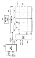
図1は、本発明の一実施例による液晶表示装置のブロック図である。図2は、本発明の一実施例による液晶表示装置の一つの画素に対する等価回路図である。また、図3は本発明の一実施例による液晶表示装置の構造図である。 FIG. 1 is a block diagram of a liquid crystal display device according to an embodiment of the present invention. FIG. 2 is an equivalent circuit diagram for one pixel of a liquid crystal display device according to an embodiment of the present invention. FIG. 3 is a structural diagram of a liquid crystal display device according to an embodiment of the present invention.
図1に示しているように、本発明の一実施例による液晶表示装置は、液晶表示板組立体300と、液晶表示板組立体300に連結されたゲート駆動部400とデータ駆動部500と、データ駆動部500に連結された階調電圧生成部800と、およびこれらを制御する信号制御部600を備える。
As shown in FIG. 1, a liquid crystal display according to an embodiment of the present invention includes a liquid
液晶表示板組立体300は等価回路でみる場合、複数の表示信号線G1〜Gn、D1〜Dm、および複数の表示信号線に連結されていてほぼ行列形態に配列された複数の画素を含む。また、液晶表示板組立体300は、互いに対向する下部表示板100及び上部表示板200と、両者の間に入っている液晶層3とを含む。
When viewed in an equivalent circuit, the liquid
表示信号線G1〜GnおよびD1〜Dmは、ゲート信号(“走査信号”とも言う)を伝達する複数のゲート線G1〜Gnと、データ信号を伝達するデータ線D1〜Dmである。ゲート線G1〜Gnは、ほぼ行方向に延びていて、互いにほとんど平行する。データ線D1〜Dmは、ほぼ列方向に延びていて、互いにほとんど平行する。 The display signal lines G 1 to G n and D 1 to D m include a plurality of gate lines G 1 to G n that transmit gate signals (also referred to as “scanning signals”) and data lines D 1 to D that transmit data signals. D m . The gate lines G 1 to G n extend substantially in the row direction and are almost parallel to each other. The data lines D 1 to D m extend substantially in the column direction and are almost parallel to each other.
各画素は、ゲート線G1〜Gn及びデータ線D1〜Dmに連結されたスイッチング素子Qと、これに連結された液晶キャパシタCLCと、ストレージキャパシタCSTとを含む。ストレージキャパシタCSTは、必要に応じて省略できる。
Each pixel includes a switching element Q connected to the
各画素のスイッチング素子Qは、下部表示板100に備えられている薄膜トランジスタなどで構成され、ゲート線G1〜Gnに連結されている制御端子と、データ線D1−Dmに連結されている入力端子と、液晶キャパシタCLC及びストレージキャパシタCSTに連結されている出力端子とを有する三端子素子である。
The switching element Q of each pixel is constituted by a thin film transistor is provided on the
液晶キャパシタCLCは、下部表示板100の画素電極190と上部表示板200の共通電極270を二つの端子とし、二つの電極190および270の間の液晶層3は誘電体として機能する。画素電極190は、スイッチング素子Qに連結され、共通電極270は上部表示板200の全面に形成されていて、共通電圧Vcomの印加を受ける。図2とは異なって、共通電極270が下部表示板100に備えられる場合は、二つの電極190、270のうちの少なくとも一つが線状もしくは棒状に形成されてもよい。
The liquid crystal capacitor C LC uses the
液晶キャパシタCLCの補助的な役割を果たすストレージキャパシタCSTは、下部表示板100に備えられた別個の信号線(図示せず)と画素電極190が絶縁体を間に置いて重なって構成され、この別個の信号線には、共通電圧Vcomなどの決められた電圧が印加される。しかし、ストレージキャパシタCSTは、画素電極190が絶縁体を媒介として直上の前端のゲート線と重なって構成されてもよい。
An auxiliary role storage capacitor C ST of the liquid crystal capacitor C LC is a separate signal line provided on the lower panel 100 (not shown)
一方、色表示を実現するために、各画素が原色のうちの一つを固有に表示(空間分割)し、各画素が時間によって交互に原色を表示(時間分割)する。これら原色の空間的、時間的な作用で所望の色相を認識させる。原色の例としては、赤色、緑色、及び青色がある。 On the other hand, in order to realize color display, each pixel uniquely displays one of the primary colors (space division), and each pixel alternately displays the primary color according to time (time division). The desired hue is recognized by the spatial and temporal effects of these primary colors. Examples of primary colors are red, green, and blue.
図2は空間分割の一例であって、各画素が上部表示板200領域に原色のうちの一つを示す色フィルター230を備えることを示している。図2とは異なって、色フィルター230は下部表示板100の画素電極190の上、もしくは画素電極190の下に形成してもよい。
FIG. 2 is an example of space division, and shows that each pixel includes a
液晶表示板組立体300の二つの表示板100、200のうち少なくとも一つの外側の面には、光を偏光させる偏光子(図示せず)が付着されている。
A polarizer (not shown) for polarizing light is attached to at least one outer surface of the two
階調電圧生成部800は、画素の透過率に関する二つの複数階調電圧を生成する。二つのうちの一つは共通電圧Vcomに対して正の値を有し、他の一つは負の値を有する。
The
ゲート駆動部400は、液晶表示板組立体300のゲート線G1〜Gnに連結されて、外部からのゲートオン電圧Vonとゲートオフ電圧Voffとの組み合わせからなるゲート信号をゲート線G1〜Gnに印加し、複数の集積回路で構成される。
The
データ駆動部500は、液晶表示板組立体300のデータ線D1〜Dmに連結されて、階調電圧生成部800からの階調電圧を選択してデータ電圧として画素に印加する。
The
ゲート駆動部400もしくはデータ駆動部500は、複数の駆動集積回路チップ形態で液晶表示板組立体300上に直接装着され、または可撓性印刷回路膜(図示せず)上に装着されてTCP(tape carrier package)形態で液晶表示板組立体300に付着されてもよい。また、ゲート駆動部400またはデータ駆動部500は、表示信号線G1〜Gn、D1〜Dmと薄膜トランジスタスイッチング素子Qと共に液晶表示板組立体300に集積されてもよい。
The
信号制御部600は、ゲート駆動部400及びデータ駆動部500などの動作を制御する。
The
以下に、このような液晶表示装置の動作について詳細に説明する。 The operation of such a liquid crystal display device will be described in detail below.
信号制御部600は、外部のグラフィック制御機(図示せず)から入力映像信号R、G、B、及びその表示を制御する入力制御信号の提供を受ける。入力制御信号は、例えば、垂直同期信号Vsync、水平同期信号Hsync、メインクロックMCLK、およびデータイネーブル信号DEなどの信号である。信号制御部600は、入力映像信号R、G、Bと入力制御信号に基づいて、入力映像信号R、G、Bを液晶表示板組立体300の動作条件に合わせて適切に処理する。また、信号制御部600は、ゲート制御信号CONT1及びデータ制御信号CONT2などの信号を生成した後、ゲート制御信号CONT1をゲート駆動部400に出力し、データ制御信号CONT2と処理した映像信号DATをデータ駆動部500に出力する。信号制御部600のデータ処理は、所定周波数を有する入力映像データR、G、Bを変換して、入力映像データR、G、Bと異なる周波数を有する複数の出力映像データを出力することを含む。信号制御部600のデータ処理については後述する。
The
ゲート制御信号CONT1は、走査開始を指示する走査開始信号STVと、ゲートオン電圧Vonの出力時間を制御する少なくとも一つのクロック信号を含む。ゲート制御信号CONT1は、ゲートオン電圧Vonの持続時間を制限する出力イネーブル信号OEを含むことができる。 The gate control signal CONT1 includes a scan start signal STV for instructing the start of scanning and at least one clock signal for controlling the output time of the gate-on voltage Von. The gate control signal CONT1 may include an output enable signal OE that limits the duration of the gate-on voltage Von.
データ制御信号CONT2は、一束の画素に対するデータの伝送を知らせる水平同期開始信号STH、データ線D1〜Dmに当該データ電圧を印加することを命令するロード信号LOAD、及びデータクロック信号HCLKを含む。また、データ制御信号CONT2は、共通電圧Vcomに対するデータ電圧の極性(以下、共通電圧に対するデータ電圧の極性を「データ電圧の極性」と称する)を反転させる反転信号RVSを含んでもよい。 The data control signal CONT2 includes a horizontal synchronization start signal STH that informs transmission of data to a bundle of pixels, a load signal LOAD that instructs application of the data voltage to the data lines D 1 to Dm, and a data clock signal HCLK. . The data control signal CONT2 may include an inversion signal RVS for inverting the polarity of the data voltage with respect to the common voltage Vcom (hereinafter, the polarity of the data voltage with respect to the common voltage is referred to as “data voltage polarity”).
信号制御部600からのデータ制御信号CONT2によって、データ駆動部500は、一行の画素に対する映像データDATを受信し、階調電圧生成部800から各映像データDATに対応する階調電圧を選択することによって、映像データDATを当該データ電圧に変換した後、これを当該データ線D1〜Dmに印加する。
In response to the data control signal CONT2 from the
ゲート駆動部400は、信号制御部600からのゲート制御信号CONT1によって、ゲートオン電圧Vonをゲート線G1〜Gnに順次に印加して、このゲート線G1〜Gnに連結されたスイッチング素子Qを導通させ、その結果データ線D1〜Dmに印加されたデータ電圧が導通したスイッチング素子Qを通じて当該画素に印加される。
The
画素に印加されたデータ電圧と共通電圧Vcomの差は、液晶キャパシタCLCの充電電圧、つまり、画素電圧として示される。液晶分子は、画素電圧の大きさに応じてその配列が異なり、そのために液晶層3を通過する光の偏光が変化する。このような偏光の変化は、表示板100、200に付着された偏光子(図示せず)によって光の透過率変化で示され、光の透過率変化によって画素の輝度が決められる。
The difference between the data voltage applied to the pixel and the common voltage Vcom is shown as the charging voltage of the liquid crystal capacitor CLC , that is, the pixel voltage. The arrangement of the liquid crystal molecules varies depending on the magnitude of the pixel voltage, and the polarization of light passing through the liquid crystal layer 3 changes accordingly. Such a change in polarization is indicated by a change in light transmittance by a polarizer (not shown) attached to the
1水平周期(1H:水平同期信号Hsync及びゲートクロックCPVの一周期)を単位として、データ駆動部500とゲート駆動部400は同一動作を繰り返す。このような方式で、一つのフレームの間に、全てのゲート線G1〜Gnに対して順次にゲートオン電圧Vonを印加して、全ての画素にデータ電圧を印加する。一つのフレームが終わると、次のフレームが始まり、各画素に印加されるデータ電圧の極性が直前フレームにおける極性と反対になるようにデータ駆動部500に印加される反転信号RVSの状態が制御される(フレーム反転)。この時、一つのフレーム内でも反転信号RVSの特性によって、一つのデータ線を通じて流れるデータ電圧の極性が変わったり(例えば、行反転、ドット反転)、隣接データ線を通じて同時に流れるデータ電圧の極性も互いに異なることがある(例えば、列反転、ドット反転)。
The
図3乃至図5を参照して、本発明の一実施例による信号制御部について詳細に説明する。 A signal control unit according to an exemplary embodiment of the present invention will be described in detail with reference to FIGS.
図3は、本発明の一実施例による信号制御部のブロック図である。図4は、図3に示した信号制御部600を含む液晶表示装置における映像データの補正前ガンマ曲線及び補正後ガンマ曲線を示したグラフである。図5は、図3に示した信号制御部600を含む液晶表示装置における映像データの補正前データ電圧と補正後データ電圧を示した波形図である。
FIG. 3 is a block diagram of a signal controller according to an embodiment of the present invention. FIG. 4 is a graph showing a pre-correction gamma curve and a post-correction gamma curve of video data in a liquid crystal display device including the
まず、図3に示されているように、信号制御部600はフレームメモリ610と、フレームメモリ610に連結されている映像信号補正部620を含む。
First, as shown in FIG. 3, the
フレームメモリ610は、入力される映像データをフレーム単位で記憶する。
The
映像信号補正部620は、フレームメモリ610に記憶されている映像データgrの入力を順次に受けて、映像データgr各々を複数の出力映像データ、例えば、第1及び第2出力映像データgr1、gr2に変換して順次に出力する。具体的に説明すると、映像信号補正部620は、映像データgrを一回ずつ読み込んで、第1出力映像データgr1に変換して順次に出力した後、映像データgrを再び一回ずつ読み込んで第2出力映像データgr2に変換して順次に出力する。その結果、データ駆動部500は、全ての画素に対して第1出力映像データgr1に相当するデータ電圧をデータ線D1〜Dmに印加した後、第2出力映像データgr2に相当するデータ電圧をデータ線D1〜Dmに印加する。以下、第1及び第2出力映像データgr1、gr2が出力される期間及び第1及び第2出力映像データgr1、gr2に相当するデータ電圧が印加される期間各々を「フィールド」と称する。
Video
一方、フレームメモリ610に記憶されている映像データを二回ずつ読み込むために、フレームメモリ610の読取り周波数(出力周波数)frは、書き取り周波数(入力周波数)fwの2倍である。その結果、フレームメモリ610の入力フレーム周波数fwが60Hzであれば、映像信号補正部620の出力フィールド周波数及びデータ電圧の印加周波数は120Hzになる。
On the other hand, in order to read the video data stored in the
一方、図4に示しているように、二つの出力映像データgr1、gr2が示すガンマ曲線T1、T2の平均は、補正前の入力映像データに対するガンマ曲線Tiと一致する。 On the other hand, as shown in FIG. 4, the average of the gamma curves T1 and T2 indicated by the two output video data g r1 and g r2 coincides with the gamma curve Ti for the input video data before correction.
これを別の表現をすれば、第1及び第2出力映像データgr1、gr2による画素の光量の合計が、補正前の入力映像データgrによる画素の光量と同一であると言える。ここで、光量とは、輝度と、その輝度を維持する時間とを乗算した値と同一である。 If the another representation which, it can be said that the sum of the first and second output image data g r1, the light amount of the pixel by g r2 is the same as the amount of pixels by the input image data g r before correction. Here, the light quantity is the same as a value obtained by multiplying the luminance and the time for maintaining the luminance.
したがって、入力映像データgrに対応する輝度をT(gr)、第1出力映像データgr1に対応する輝度をT(gr1)、および第2出力映像データgr2に対応する輝度をT(gr2)とすると、以下の式(1)が成立する。 Accordingly, luminance T (g r) corresponding to the input image data g r, the luminance corresponding to the first output image data g r1 T (g r1), and the corresponding luminance to the second output image data g r2 T Assuming (g r2 ), the following equation (1) is established.
2T(gr)=T(gr1)+T(gr2)・・・(1)
このように一つの入力映像データgrを二つの出力映像データgr1、gr2に変換する場合、二つの出力映像データgr1、gr2のうちの一つは、他の一つより大きいか、または同一である。二つの出力映像データの中で大きいものを先に出力し、小さいものを後に出力し、またはその反対にすることもできる。ノーマリーブラックモード液晶表示装置の場合、映像データが大きければ相当するデータ電圧もまた大きい。図5の(b)に、ノーマリーブラックモード液晶表示装置において、二つの出力映像データgr1、gr2の中で大きいものを先に出力し、小さいものを後に出力する場合のデータ電圧を示した。図5の(a)は、入力映像データを補正せずにそのまま出力した場合のデータ電圧を示す。
2T (g r ) = T (g r1 ) + T (g r2 ) (1)
When one input video data g r is converted into two output video data g r1 and g r2 in this way, is one of the two output video data g r1 and g r2 larger than the other one? Or the same. Of the two output video data, the larger one can be output first and the smaller one can be output later, or vice versa. In the case of a normally black mode liquid crystal display device, if the video data is large, the corresponding data voltage is also large. FIG. 5B shows a data voltage in the normally black mode liquid crystal display device in which the larger one of the two output video data g r1 and g r2 is output first and the smaller one is output later. It was. FIG. 5A shows the data voltage when the input video data is output as it is without correction.
二つの出力映像データgr1、gr2のうち低い方を0、または0に近くすることで、インパルシブ駆動の効果を得ることができる。
By making the lower one of the two output video data g r1 and
次に、図6を参照して、本発明の他の実施例による信号制御部について詳細に説明する。 Next, a signal controller according to another embodiment of the present invention will be described in detail with reference to FIG.
図6は、本発明の他の実施例による信号制御部のブロック図である。 FIG. 6 is a block diagram of a signal controller according to another embodiment of the present invention.
図6に示しているように、本実施例による信号制御部600は、第1フレームメモリ630と映像信号補正部640を含む。映像信号補正部640は、フレームメモリ630と連結されている信号変換部641、信号変換部641に連結されている第2フレームメモリ642、および信号変換部641及び第2フレームメモリ642に連結されているDCC処理部643を備える。
As shown in FIG. 6, the
第一フレームメモリ630及び信号変換部641の動作は、図3に示した信号制御部のフレームメモリ610及び映像信号補正部620の動作と同一である。
The operations of the
つまり、第一フレームメモリ630は、第1周波数fwで入力される映像データをフレーム単位で記憶する。信号変換部641は、第一フレームメモリ630に記憶されている映像データgrを第1周波数fwの2倍である第2周波数frで順次に読み込んで、映像データgr各々を第1及び第2臨時映像データgr1、gr2に変換して順次に出力する。変換の原理は、図4及び図5を参照して説明した通りである。
That is, the
第2フレームメモリ642は、信号変換部641からの臨時映像データgr1、gr2を二つのフィールド単位で記憶する。つまり、二つのフィールドの映像データを記憶する。
The second frame memory 642 stores the temporary video data g r1 and g r2 from the
DCC処理部643は、信号変換部641からの映像データと第2フレームメモリ642からの映像データを受信する。この時、第2フレームメモリ642から出力される映像データは、直前フレームの映像データ(以下「直前映像データ」と称し、gr−1と表記する)である。直前映像データと区分するために、信号変換部641からの映像データを現在フレームの映像データ(以下、「現在映像データ」と称する。)とする。
The
DCC処理部643は、現在映像データgr1、gr2各々を直前映像データgr−1,1、gr−1,2と比較する。比較した結果によって、現在映像データgr1、gr2を出力映像データgr1´、gr2´に変換する。出力映像データは、現在映像データと直前映像データの大きさの差であり、これをDCCという。
The
例えば、現在映像データgr1、gr2が直前映像データgr−1,1、gr−1,2より大きい場合、つまり、gr,p>gr−1,p(p=1、2)である場合、出力映像データgr1´、gr2´は、現在映像データgr1、gr2より大きい。反対に、現在映像データgr1、gr2が直前映像データgr−1,1、gr−1,2より小さい場合、つまり、gr,p<gr−1,pである場合、出力映像データgr1´、gr2´は現在映像データgr1、gr2より小さい。また、現在映像データgr1、gr2が直前映像データgr−1,1、gr−1,2と同一である場合、つまり、gr,p=gr−1,pである場合、出力映像データgr1´、gr2´は、現在映像データgr1、gr2と同一である。 For example, when the current video data g r1 and g r2 are larger than the previous video data g r-1,1 , g r-1,2 , that is, g r, p > g r-1, p (p = 1, 2). If) is, output image data g r1 ', g r2' is greater than the current image data g r1, g r2. On the other hand, if the current video data g r1 and g r2 are smaller than the previous video data g r−1,1 and g r−1 , that is, if g r, p <g r−1, p , the output image data g r1 ', g r2' is now smaller than the image data g r1, g r2. Also, if the current video data g r1 and g r2 are the same as the previous video data g r-1,1 , g r-1,2 , i.e., if g r, p = g r-1, p , output image data g r1 ', g r2' is the same as the current image data g r1, g r2.
現在映像データgr1、gr2が直前映像データgr−1,1、gr−1,2と異なる場合、出力映像データgr1´、gr2´を現在映像データgr1、gr2より大きく、または小さくするので、相当する画素が目標輝度に速かに接近することができる。 The current image data g r1, g r2 is the previous image data g r-1,1, if different from the g r-1,2, the output image data g r1 ', greater than g r2' the current image data g r1, g r2 Alternatively, the corresponding pixel can quickly approach the target luminance.
図7乃至図9を参照して、本発明の他の実施例による信号制御部について詳細に説明する。 A signal controller according to another embodiment of the present invention will be described in detail with reference to FIGS.
図7は、本発明の他の実施例による信号制御部のブロック図である。図8は、図7に示した信号制御部を含む液晶表示装置の時間に応じた透過率変化を示したグラフである。図9は、図3に示した信号制御部を含む液晶表示装置の時間に応じた透過率変化を示したグラフである。 FIG. 7 is a block diagram of a signal controller according to another embodiment of the present invention. FIG. 8 is a graph showing a change in transmittance according to time of the liquid crystal display device including the signal control unit shown in FIG. FIG. 9 is a graph showing a change in transmittance according to time of the liquid crystal display device including the signal control unit shown in FIG.
まず、図7に示しているように、本実施例による信号制御部600はフレームメモリ650と、フレームメモリ650に連結されている映像信号補正部660とを含む。
First, as shown in FIG. 7, the
フレームメモリ650は、第1周波数fwで入力される映像データを二つのフレームで記憶する。
The
映像信号補正部660は、フレームメモリ650に記憶されている直前入力映像データgr−1と現在入力映像データgrとを第1周波数の2倍である第2周波数frで順次に読み込み、現在入力映像データgr各々を直前入力映像データgr−1と比較し、比較した結果によって、現在入力映像データgrを第1及び第2出力映像データgr1´、gr2´に変換する。
Video
この時、第1出力映像データgr1´は、現在入力映像データgrと直前入力映像データgr−1との大きさの差によって、前記図6を参照して説明した第1臨時映像データgr1(または、図3を参照して説明した映像信号補正部620の第1出力映像データgr1)より大きいか小さいか同一である。
At this time, the first output image data g r1 'is the magnitude difference between the current input image data g r and the previous input image data g r-1, the first provisional image data described with reference to FIG. 6 It is larger or smaller than g r1 (or the first output video data g r1 of the video
例えば、現在入力映像データgrが直前入力映像データgr−1より大きい場合、つまり、gr>gr−1である場合、第1出力映像データgr1´は第1臨時映像データgr1より大きい。反対に、現在入力映像データgrが直前入力映像データgr−1より小さい場合、つまり、gr<gr−1である場合、第1出力映像データgr1´は第1臨時映像データgr1より小さい。また、現在入力映像データgr1、gr2が直前入力映像データgr−1,1、gr−1,2と同一である場合、つまり、gr=gr−1である場合、第1出力映像データgr1´は第1臨時映像データgr1と同一である。 For example, when the current input video data g r is larger than the previous input video data g r−1 , that is, when g r > g r−1 , the first output video data g r1 ′ is the first temporary video data g r1. Greater than. Conversely, if the current input image data g r is the previous input image data g r-1 less than, i.e., g r <If a g r-1, the first output image data g r1 'is first provisional image data g smaller than r1 . If the current input video data g r1 and g r2 are the same as the previous input video data g r−1,1 and g r−1 , that is, if g r = g r−1 , the first output image data g r1 'is identical to the first provisional image data g r1.
このように、現在入力映像データgr1、gr2が直前入力映像データgr−1,1、gr−1,2と異なる場合、第1出力映像データgr1´を第1臨時映像データgr1より大きく、または小さくするので、相当する画素が目標輝度に速かに接近することができる。 As described above, when the current input video data g r1 and g r2 are different from the previous input video data g r-1,1 , g r-1,2 , the first output video data g r1 ′ is changed to the first temporary video data g. Since it is larger or smaller than r1 , the corresponding pixel can quickly approach the target luminance.
しかし、第2出力映像データgr2´を決める時には、第1出力映像データgr1´を求める方法であるDCCを適用しない。特に、第2出力映像データgr2´が0、または0に近い値であるとき、第2出力映像データgr2´が第2臨時映像データgr2と同一であり得る。
However, when determining the second output video data g r2 ′ , DCC, which is a method for obtaining the first output video data g r1 ′ , is not applied. In particular, when the second
第2出力映像データgr2´は、実験などを通じて既に決められた値とするが、例えば、第1臨時映像データgr1と第2臨時映像データgr2とに相当するデータ電圧を、引続き画素に印加する時に得られる最終的な平衡状態の透過率曲線に、最も速く到達できる値に決める。具体的に説明すると、入力映像データがr番目フレームで、(r−1)番目フレームから変わった後に、その次の(r+1)番目フレームからは変化しないと仮定する場合、最終的に示される平衡状態の透過率曲線が最も速い。可能であれば、(r+1)番目フレームから示されるように第2出力映像データgr2´を決める。 Second output image data g r2 'is the previously determined value through experiments or the like, for example, a data voltage corresponding to the first provisional image data g r1 and the second provisional image data g r2, continue to the pixel The final equilibrium transmission curve obtained when applied is determined to be the fastest possible value. More specifically, when it is assumed that the input video data is the r-th frame and has not changed from the (r + 1) -th frame after it has changed from the (r-1) -th frame, the equilibrium shown finally The state transmittance curve is the fastest. If possible, the second output video data gr2 ′ is determined as shown from the (r + 1) th frame.
このように決められた第1及び第2出力映像データを適用した液晶表示装置の透過率が図8に示した。図9は、図3を参照して説明した第1及び第2出力映像データを適用した液晶表示装置の透過率が示されている。 FIG. 8 shows the transmittance of the liquid crystal display device to which the first and second output video data determined in this way are applied. FIG. 9 shows the transmittance of the liquid crystal display device to which the first and second output video data described with reference to FIG. 3 is applied.
図8及び図9において、Ti1とTi2は入力映像データを補正しなかった場合に現れる画素の予想透過率を示し、Ttは入力映像データを補正した場合に現れる画素の予想透過率を示し、Taは入力映像データを補正した場合に現れる画素の実際透過率を示す。TtとTaが異なることは、液晶の応答速度が遅いためである。したがって、DCC処理を行うわけである。 8 and 9, T i1 and T i2 indicate the expected transmittance of the pixel that appears when the input video data is not corrected, and Tt indicates the expected transmittance of the pixel that appears when the input video data is corrected. , Ta indicate the actual transmittance of pixels that appear when the input video data is corrected. The difference between Tt and Ta is because the response speed of the liquid crystal is slow. Therefore, DCC processing is performed.
図8に示しているように、第1出力映像データに対しては、DCCを適用し、第2出力映像データに対しては、DCCを適用せずに平衡状態に速く到達できるようにする値に決めた場合、入力映像データが変化したr番目フレームの直後フレームである(r+1)番目フレームから透過率曲線Taが平衡状態に到達する。 As shown in FIG. 8, a value that allows DCC to be applied to the first output video data, and allows the equilibrium state to be reached quickly without applying DCC to the second output video data. In this case, the transmittance curve Ta reaches an equilibrium state from the (r + 1) th frame which is the frame immediately after the rth frame in which the input video data has changed.
これに反し、DCCを全く適用しなかった図9では、透過率曲線Taはいくつものフレーム間で引続き変化する。 On the other hand, in FIG. 9 where no DCC is applied, the transmittance curve Ta continues to change between several frames.
一つの入力映像データを二つの出力映像データに変換する場合について、上述の通り説明したが、その他の場合にも上述した説明で適用できる。例えば、一つの映像データを三つの出力映像データに変換する場合、出力周波数は入力周波数の3倍になって、最大輝度を与える出力映像データのみにDCCを適用し、残りは実験やその他によって得たものであり得る。また、四つの入力映像データを3対の出力映像データに変換することもでき、この時にもDCCは最も大きい値に対してのみ適用できる。 Although the case where one input video data is converted into two output video data has been described as described above, the above description can also be applied to other cases. For example, when one video data is converted into three output video data, the output frequency is three times the input frequency, and the DCC is applied only to the output video data giving the maximum luminance, and the rest is obtained by experiments and others. Can be. Also, the four input video data can be converted into three pairs of output video data, and the DCC can be applied only to the largest value at this time as well.
次に、図10及び図11を参照して、図7に示した映像信号補正部の例について詳細に説明する。 Next, an example of the video signal correction unit illustrated in FIG. 7 will be described in detail with reference to FIGS. 10 and 11.
図10及び図11は、図7に示した映像信号補正部のブロック図の例である。 10 and 11 are examples of block diagrams of the video signal correction unit shown in FIG.
図10に示した映像信号補正部660は、ルックアップテーブルL1と、ルックアップテーブルL1と連結されていてフィールド選択信号FSの入力を受けるマルチプレクサー661とを含む。フィールド選択信号FSは、多様な方式で決めることができるが、単純にフィールドの奇数偶数で決める、またはカウンターなどを使って決めることもできる。また、このフィールド選択信号FSは、信号制御部600内部で生成されることもできるし、外部から提供されてもよい。
The video
ルックアップテーブルL1には、図7を参照して上述に説明した方法と同じ方法で求めた第1及び第2出力映像データgr1´、gr2´が直前入力映像データgr−1と現在入力映像データgrの関数で記憶されている。したがって、ルックアップテーブルL1は直前入力映像データgr−1と現在入力映像データgrに対応する第1及び第2出力映像データgr1´、gr2´をマルチプレクサー661に出力する。
The lookup table L1, first and second output image data g r1 'calculated in the same manner as described in above with reference to FIG. 7, g r2' is the previous input image data g r-1 and current It is stored as a function of the input image data g r. Accordingly, the look-up table L1 outputs the first and second output video data g r1 ′ and g r2 ′ corresponding to the immediately previous input video data g r−1 and the current input video data g r to the
マルチプレクサー661は、フィールド選択信号FSの値によってルックアップテーブルL1からの第1及び第2出力映像データgr1´、gr2´の中で一つを選択して出力する。
The
図11に示した映像信号補正部660は、第1ルックアップテーブルL21と、第2ルックアップテーブルL22と、ルックアップテーブルL21及びL22に連結されていてフィールド選択信号FSの入力を受けるマルチプレクサー662と、マルチプレクサー662に連結された第3ルックアップテーブルL23とを含む。
The video
第1ルックアップテーブルL21及び第2ルックアップテーブルL22には、図7を参照して上述に説明した方法と同じ方法で求めた第1及び第2出力データgr1´、gr2´が各々記憶されている。 The first look-up table L21 and the second look-up table L22 store first and second output data g r1 ′ and g r2 ′ obtained by the same method as described above with reference to FIG. Has been.
マルチプレクサー662は、一つのフィールドが終わって次のフィールドが始まる前にフィールド選択信号FS値によって、第1ルックアップテーブルL1及び第2ルックアップテーブルL22からの第1及び第2出力映像データgr1´、gr2´の中で一つを選択して出力する。
The
第3ルックアップテーブルL23は、マルチプレクサー662からの第1及び第2出力映像データgr1´、gr2´を直前入力映像データgr−1と現在入力映像データgrの関数で記憶し、入力された直前入力映像データgr−1と現在入力映像データgrに対応する第1もしくは第2出力映像データgr1´、gr2´を出力する。
The third lookup table L23 stores a function of the first and second output image data g r1 ', previous input image data g r2' g r-1 and current input image data g r from the
この場合、原色、例えば赤色、緑色及び青色の三原色別に同一ルックアップテーブルを使用し、これら三原色のDCC変換が同時に行われると、全ルックアップテーブルの大きさを縮小するのに有利である。 In this case, if the same lookup table is used for each of the primary colors, for example, red, green, and blue, and DCC conversion of these three primary colors is performed simultaneously, it is advantageous to reduce the size of the entire lookup table.
以下に、図12及び図14を参照して、図7に示した信号制御部を含む液晶表示装置において、出力映像データを決める他の方法について詳細に説明する。 Hereinafter, another method for determining output video data in the liquid crystal display device including the signal control unit shown in FIG. 7 will be described in detail with reference to FIGS.
本実施例では、ルックアップテーブルに直前映像データ及び現在映像データの一部値(または階調)に対して出力映像データと関する係数が記憶されており、映像信号補正部は、この係数を使用して出力映像データを求める。これについて詳細に説明する。 In this embodiment, the coefficient relating to the output video data is stored in the lookup table with respect to the partial value (or gradation) of the previous video data and the current video data, and the video signal correction unit uses this coefficient. To obtain output video data. This will be described in detail.
図12は、図7に示した信号制御部を含む液晶表示装置で出力映像データを決める他の方法を説明するための図面である。 FIG. 12 is a diagram for explaining another method of determining output video data in the liquid crystal display device including the signal control unit shown in FIG.
説明の便宜のために、入力映像データがxビットの上位ビット(MSB)とyビットの下位ビット(LSB)からなると仮定する。 For convenience of explanation, it is assumed that the input video data is composed of an x-bit upper bit (MSB) and a y-bit lower bit (LSB).
例えば、8ビット映像信号の場合、階調数が256個であるので、直前入力映像データgr−1と現在入力映像データgrの組み合わせは全て256×256=65,536個となる。多くの数の組み合わせ各々に対して最終出力映像データgr1´、gr2´をルックアップテーブルに記憶しておくことは、時間的、空間的に無理がある。したがって、直前入力映像データ及び現在入力映像データの一部対に対する出力映像データgr1´、gr2´をルックアップテーブルに記憶しておき、これを基準に、残り対に対する出力映像データgr1´、gr2´を求める方式を補間という。特に下位ビットが0である直前入力映像データ及び現在入力映像データの対に対する出力映像データgr1´、gr2´を記憶しておいて、これを基準に他の入力映像データ対に対する出力映像データgr1´、gr2´を求めることは比較的に簡単である。 For example, in the case of 8-bit video signal, the number of gradations is 256, a combination of previous input image data g r-1 and current input image data g r are all 256 × 256 = 65,536 pieces. It is impossible in terms of time and space to store the final output video data g r1 ′ and g r2 ′ in a lookup table for each of a large number of combinations. Accordingly, the output video data g r1 ′ and g r2 ′ for a partial pair of the previous input video data and the current input video data are stored in the lookup table, and the output video data g r1 ′ for the remaining pairs is stored based on this. , G r2 ′ is called interpolation. In particular, output video data g r1 ′ and g r2 ′ for a pair of the previous input video data and the current input video data whose lower bits are 0 are stored, and output video data for other input video data pairs based on this. It is relatively simple to obtain g r1 ′ and g r2 ′ .
8ビット映像データである場合、上位ビットのビット数は4または3とすることができるが、上位ビットのビット数が4である場合、17×17の入力映像データ対、3である場合には9×9の入力データ対に対する出力映像データgr1´、gr2´のみを記憶すればよい。 In the case of 8-bit video data, the number of high-order bits can be 4 or 3. However, when the number of high-order bits is 4, 17 × 17 input video data pairs, Only the output video data g r1 ′ and g r2 ′ for the 9 × 9 input data pair need be stored.
上位ビットのビット数が4である場合に対して、図12に示したように、横軸と縦軸に各々直前入力映像データgr−1と現在入力映像データgrを配置してみる。 For the case the number of bits of the upper bits is 4, as shown in FIG. 12, with each previous input image data g r-1 in the horizontal and vertical axes try to place the current input image data g r.
図12における実線で区画された正方形領域は、直前入力映像データgr−1と現在入力映像データgrの上位ビットの値を基準に分けられたブロックである。ブロックの境界に存在する点は、直前入力映像データgr−1または現在入力映像データgrの下位ビットが0の点である。直前入力映像データgr−1と現在入力映像データgr全てに対して各ブロック内に存在する点の上位ビットは全て同一であり、左側辺と上側辺上に位置する点もブロック内部の点と同一な上位ビットを有する。ただし、右側辺と下側辺上に存在する点の上位ビットは、ブロック内部点の上位ビットと相異なる。 Square region defined by the solid line in FIG. 12 is a block which is divided into the previous input image data g r-1 based on the value of the upper bits of the current input image data g r. Points existing in the block boundary, the lower bits of the previous input image data g r-1 or current input image data g r is a point of zero. All the previous input image data g r-1 high-order bits of points existing in each block for the current input image data g r are all the same, in terms of the internal block also points situated on the left side and the upper side Have the same high order bits. However, the upper bits of the points existing on the right side and the lower side are different from the upper bits of the block internal point.
各ブロックの頂点に対しては、出力映像データが与えられ、これを基準データfと称する。例えば、図12は、一つのブロックを定義する四つの頂点に対する出力映像データをf00、f01、f10、f11で示している。頂点でない点に対する出力映像データは、これらと下位ビットの関数で与えられる演算を通じて求める。 Output video data is given to the vertices of each block, which is referred to as reference data f. For example, FIG. 12 shows output video data for four vertices defining one block as f 00 , f 01 , f 10 , and f 11 . Output video data for a point that is not a vertex is obtained through an operation given by a function of these and a lower bit.
このような補間法の例を以下に説明する。 An example of such an interpolation method will be described below.
現在入力映像データgrの上位ビット及び下位ビットを各々gr[x+y−1:y]、gr[y−1:0]とし、直前入力映像データgr−1の上位ビット及び下位ビットを各々gr−1[x+y−1:y]、gr−1[y−1:y」とすれば、基準データfは以下の数式(2)で示すことができる。 Each g r the upper and lower bits of the current input image data g r [x + y-1 : y], g r [y-1: 0] and then, the upper and lower bits of the previous input image data g r-1 If g r-1 [x + y-1: y] and g r-1 [y-1: y] are used, the reference data f can be expressed by the following mathematical formula (2).
f(gr[x+y−1:y]、gr−1[x+y−1:y]=gr´(gr[x+y−1:y]×2y、gr−1[x+y−1:y]×2y)・・・(2)
ここで、gr´はgr1´またはgr2´である。
f (g r [x + y -1: y], g r-1 [x + y-1: y] = g r'(g r [x + y-1: y] × 2 y, g r-1 [x + y-1: y] × 2 y ) (2)
Here, g r ′ is g r1 ′ or g r2 ′ .
上述した図12のブロック内点に対する出力映像データgr´は次の数式(3)のような補間法で与えられる。 Output image data g r'for block point in FIG. 12 described above are given by interpolation as in Equation (3).
g=f00+p×gr−1[y−1:0]/2y+q×gr[y−1:0]/2y+r×gr−1[y−1:0]×gr[y−1:0]/22y・・・(3)
ここで、αとβは各々直前入力映像信号gr−1と現在入力映像データgrの下位ビットをブロック間隔2yで分けた値である(0≦α<1、0≦β<1)。
g = f 00 + p × g r-1 [y-1: 0] / 2 y + q × g r [y-1: 0] / 2 y + r × g r-1 [y-1: 0] × g r [Y-1: 0] / 2 2y (3)
Here, the alpha and beta is a value obtained by dividing the lower bits of each previous input image signal g r-1 and current input image data g r in block interval 2 y (0 ≦ α <1,0 ≦ β <1) .
ここで、p、q、rは以下の数式(4)、(5)、(6)で示す。 Here, p, q, and r are shown by the following mathematical formulas (4), (5), and (6).
p(gr[x+y−1:y]、gr−1[x+y−1:y])=f01−f00=f(gr[x+y−1:y]、gr−1[x+y−1:y]+1)−f(gr[x+y−1:y]、gr−1[x+y−1:y]・・・(4)
q(gr[x+y−1:y]、gr−1[x+y−1:y])=f10−f00=f(gr[x+y−1:y]+1、gr−1[x+y−1:y])−f(gr[x+y−1:y]、gr−1[x+y−1:y])・・・(5)
r(gr[x+y−1:y]、gr−1[x+y−1:y])=f00+f11−f01−f10=f(gr[x+y−1:y]、gr−1[x+y−1:y])+f(gr[x+y−1:y]+1、gr−1[x+y−1:y]+1)−f(gr[x+y−1:y]、gr−1[x+y−1:y]+1)−f(gr[x+y−1:y]+1、gr−1[x+y−1:y])・・・(6)
ルックアップテーブルには、基準データfのみを記憶しておき、その他のp、q、およびrなどの係数は、演算を通じて求めることができる。しかし、演算時間が長くかかる短所があるため、基準データfの他にもp、q、およびrなどの係数を記憶しておけば演算時間が節約される。
p (g r [x + y -1: y], g r-1 [x + y-1: y]) = f 01 -f 00 = f (g r [x + y-1: y], g r-1 [x + y- 1: y] +1) -f ( g r [x + y-1: y], g r-1 [x + y-1: y] ··· (4)
q (g r [x + y -1: y], g r-1 [x + y-1: y]) = f 10 -f 00 = f (g r [x + y-1: y] + 1, g r-1 [x + y −1: y]) − f (g r [x + y−1: y], g r−1 [x + y−1: y]) (5)
r (g r [x + y -1: y], g r-1 [x + y-1: y]) = f 00 + f 11 -f 01 -
Only the reference data f is stored in the lookup table, and other coefficients such as p, q, and r can be obtained through calculation. However, since the calculation time is long, if the coefficients such as p, q, and r are stored in addition to the reference data f, the calculation time is saved.
このような方式によって、入力映像データgrに対する第1出力映像データgr1´と第2出力映像データgr2´を求める。ただし、前記数式は一つの例に過ぎず、他の方法で補間を行ってもよい。 Such a scheme, obtaining the first output image data g r1 'and the second output image data g r2' for the input image data g r. However, the mathematical formula is only an example, and interpolation may be performed by other methods.
図13と図14には、このような原理に基づいて補正を行う映像信号補正部の例が示されている。 FIGS. 13 and 14 show an example of a video signal correcting unit that performs correction based on such a principle.
図13及び図14は、本発明の他の実施例による映像信号補正部のブロック図の例である。 13 and 14 are block diagram examples of a video signal correction unit according to another embodiment of the present invention.
図13に示した映像信号補正部660は、ルックアップテーブルL3と、これに連結されていてフィールド選択信号FSの入力を受けるマルチプレクサー663と、マルチプレクサー663に連結されていて直前映像データgr−1及び現在入力映像データgrの入力を受ける演算部664とを含む。
ルックアップテーブルL3には、第1出力映像データgr1´に対する基準データf1及び係数p1、q1、r1(以下、二つを合せて第1補正係数と言う)と、第2出力映像データgr2´に対する基準データf2及び係数p2、q2、r2(以下、二つを合せて第2補正係数と言う)とが直前入力映像データgr−1と現在入力映像データgrの関数で記憶されている。したがって、ルックアップテーブルL3は、直前入力映像データgr−1と現在入力映像データgrに応答して、これに対応する第1補正係数f1、p1、q1、r1と第2補正係数f2、p2、q2、r2をマルチプレクサー663に出力する。
The look-up table L3 includes reference data f 1 and coefficients p 1 , q 1 , r 1 (hereinafter referred to as the first correction coefficient together) for the first output video data g r1 ′ and the second output. reference data f 2 and
マルチプレクサー663は、フィールド選択信号FS値によってルックアップテーブルL1からの第1補正係数f1、p1、q1、r1と第2補正係数f2、p2、q2、r2のうちの一つを選択して出力する。
The
演算部664は、マルチプレクサー663からの第1または第2補正係数f1、p1、q1、r1、f2、p2、q2、r2と直前及び現在入力映像データgr−1、grの下位ビットの入力を受けて数式(3)の演算を行い、第1出力映像データgr1´や第2出力映像データgr2´を生成して出力する。
The
このように補間法によって出力映像データgr1´、gr2´を生成すれば、ルックアップテーブルの大きさとデータ処理時間などを大きく縮小することができる。 If the output video data g r1 ′ and g r2 ′ are generated by the interpolation method in this way, the size of the lookup table and the data processing time can be greatly reduced.
図14に示した映像信号補正部660は、第1ルックアップテーブルL41と、第2ルックアップテーブルL42と、これらルックアップテーブルL41及びL42に各々連結されていてフィールド選択信号FSの入力を受けるマルチプレクサー665と、マルチプレクサー665に連結されていて直前入力映像データgr−1と現在入力映像データgrの入力を受ける第3ルックアップテーブルL43と、第3ルックアップテーブルL43に連結されていて直前入力映像データgr−1と現在入力映像データgrの入力を受ける演算部666と、を含む。
The video
第1ルックアップテーブルL41及び第2ルックアップテーブルL42には上述した第1及び第2補正係数が各々記憶されている。 The first and second correction coefficients are stored in the first lookup table L41 and the second lookup table L42, respectively.
マルチプレクサー665は、一つのフィールドが終わって次のフィールドが始まる前にフィールド選択信号FS値によって第1ルックアップテーブルL41及び第2ルックアップテーブルL42からの第1及び第2補正係数の中で一つを選択して出力する。
The
第3ルックアップテーブルL43は、マルチプレクサー663からの第1または第2補正係数を直前入力映像データgr−1と現在入力映像データgrの関数で記憶し、入力された直前入力映像データgr−1と現在入力映像データgrに応答して相当する第1または第2補正係数を出力する。
The third lookup table L43 stores the first or second correction coefficient from the
演算部666は、マルチプレクサー665からの第1または第2補正係数f1,p1、q1、r1、f2、p2、q2、r2と直前及び現在入力映像データgr−1、grの下位ビットの入力を受けて数式(3)の演算を行い、第1出力映像データgr1´、または第2出力映像データgr2´を生成して出力する。
The
この場合にも、図11に示しているように、例えば、赤色、緑色及び青色の三原色別に同一ルックアップテーブルを使用し、これら三原色のDCC変換が同時に行われる場合、全ルックアップテーブルの大きさを縮小するのに有利である。 Also in this case, as shown in FIG. 11, for example, when the same lookup table is used for each of the three primary colors of red, green, and blue, and the DCC conversion of these three primary colors is performed simultaneously, the size of the entire lookup table It is advantageous to reduce.
上述に、一つの入力映像データを二つの出力映像データに変換する場合について説明したが、その他の場合にも上述した説明で適用できる。例えば、一つの映像データを三つの出力映像データに変換することができ、この時出力周波数は入力周波数の3倍になり、最大輝度を与える出力映像データのみDCCを適用し得て、残りは実験やその他によって得られたものであってもよい。これとは異なって、四つの入力映像データを3対の出力映像データに変換することもでき、この時にもDCCは最も大きい値に対してのみ適用できる。 Although the case where one input video data is converted into two output video data has been described above, the above description can also be applied to other cases. For example, one video data can be converted into three output video data. At this time, the output frequency is three times the input frequency, and only the output video data giving the maximum luminance can be applied with DCC, and the rest is an experiment. Or may be obtained by others. In contrast to this, four input video data can be converted into three pairs of output video data, and the DCC can be applied only to the largest value.
以上、本発明の好ましい実施例について詳細に説明したが、本発明の権利範囲はこれに限定されず、請求範囲で定義している本発明の基本概念を利用した当業者の様々な変形及び改良形態もまた本発明の権利範囲に属する。 The preferred embodiments of the present invention have been described in detail above, but the scope of the present invention is not limited thereto, and various modifications and improvements of those skilled in the art using the basic concept of the present invention defined in the claims. Forms are also within the scope of the present invention.
3 液晶層、
100、200 基板、
230 色フィルター、
270 共通電極、
300 液晶表示板組立体、
400 ゲート駆動部、
500 データ駆動部、
600 信号制御部、
800 階調電圧生成部、
G1−Gn ゲート線、
D1−Dm データ線、
Q スイッチング素子、
CLC 液晶キャパシタ、
CST ストレージキャパシタ、
610 フレームメモリ、
620 映像補正部、
630、642、650 フレームメモリ、
640 映像信号補正部、
641 信号変換部、
643 DCC処理部、
660 映像信号補正部、
L21、L22、L23、L41、L42、L43 ルックアップテーブル、
662、663、665 マルチプレクサー、
664、666 演算部。
3 liquid crystal layer,
100, 200 substrates,
230 color filters,
270 common electrode,
300 LCD panel assembly,
400 gate driver,
500 data driver,
600 signal control unit,
800 gradation voltage generator,
G 1 -G n gate line,
D 1 -D m data lines,
Q switching element,
C LC liquid crystal capacitor,
C ST storage capacitor,
610 frame memory,
620 video correction unit,
630, 642, 650 frame memory,
640 video signal correction unit,
641 signal converter,
643 DCC processing unit,
660 video signal correction unit,
L21, L22, L23, L41, L42, L43 lookup table,
662, 663, 665 multiplexer,
664, 666 arithmetic unit.
Claims (33)
第1周波数の入力映像データを第2周波数の複数の出力映像データに変換して出力する信号制御部と、
前記信号制御部からの前記複数の出力映像データ各々をアナログデータ電圧に変換して前記画素に、順次に印加するデータ駆動部と、を含み、
前記複数の出力映像データのうちの前記画素に最大輝度を与える出力映像データである最大出力映像データは、前記入力映像データを直前フレームの入力映像データである直前入力映像データと比較して決められる表示装置の駆動装置。 A device for driving a display device including a plurality of pixels arranged in a matrix form,
A signal control unit for converting the input video data of the first frequency into a plurality of output video data of the second frequency and outputting the data;
A data driving unit that converts each of the plurality of output video data from the signal control unit into an analog data voltage and sequentially applies the converted data to the pixels;
The maximum output video data that is the output video data that gives the maximum luminance to the pixels among the plurality of output video data is determined by comparing the input video data with the previous input video data that is the input video data of the previous frame. Drive device for display device.
前記第1出力映像データは、前記第2出力映像データより大きい請求項2に記載の表示装置の駆動装置。 The plurality of output video data includes first output video data and second output video data,
The display device driving apparatus according to claim 2, wherein the first output video data is larger than the second output video data.
前記入力映像データと前記直前入力映像データとを記憶するフレームメモリと、
前記フレームメモリからの前記入力映像データを前記直前入力映像データと比較して、前記入力映像データを前記第1出力映像データ及び第2出力映像データに変換して出力する映像信号補正部と、
を含む請求項7に記載の表示装置の駆動装置。 The signal controller is
A frame memory for storing the input video data and the immediately preceding input video data;
A video signal correction unit that compares the input video data from the frame memory with the immediately preceding input video data, converts the input video data into the first output video data and the second output video data, and outputs the video signal correction unit;
The drive device of the display apparatus of Claim 7 containing.
前記第1出力映像データ及び第2出力映像データが記憶されているルックアップテーブルと、
制御信号によって前記ルックアップテーブルからの第1出力映像データ及び第2出力映像データのうちの一つを選択して出力するマルチプレクサーと、
を含む請求項13に記載の表示装置の駆動装置。 The video signal correction unit is
A lookup table in which the first output video data and the second output video data are stored;
A multiplexer that selects and outputs one of the first output video data and the second output video data from the lookup table according to a control signal;
The display device drive device according to claim 13, comprising:
前記第1出力映像データ及び第2出力映像データが、各々記憶されている第1ルックアップテーブル及び第2ルックアップテーブルと、
制御信号によって前記第1ルックアップテーブル及び第2ルックアップテーブルからの第1出力映像データ及び第2出力映像データのうちの一つを選択して出力するマルチプレクサーと、
前記マルチプレクサーからの第1出力映像データもしくは第2出力映像データを、前記入力映像データと前記直前入力映像データの関数で記憶し、前記入力映像データと前記直前入力映像データに対応する第1出力映像データもしくは第2出力映像データを出力する第3ルックアップテーブルと、
を含む請求項13に記載の表示装置の駆動装置。 The video signal correction unit is
A first lookup table and a second lookup table in which the first output video data and the second output video data are respectively stored;
A multiplexer that selects and outputs one of the first output video data and the second output video data from the first lookup table and the second lookup table according to a control signal;
First output video data or second output video data from the multiplexer is stored as a function of the input video data and the previous input video data, and a first output corresponding to the input video data and the previous input video data. A third lookup table for outputting video data or second output video data;
The display device drive device according to claim 13, comprising:
前記入力映像データと前記直前入力映像データとを記憶するフレームメモリと、
前記フレームメモリからの前記入力映像データと前記直前入力映像データとに基づいて前記入力映像データを前記複数の出力映像データに変換して出力する映像信号補正部と、
を含み、
前記映像信号補正部は、前記直前入力映像データと前記入力映像データとの一部対に対する出力映像データを記憶しているルックアップテーブルをさらに含み、残り直前入力映像データと残り入力映像データとの対に対する出力映像データは補間方式で求められる請求項1に記載の表示装置の駆動装置。 The signal controller is
A frame memory for storing the input video data and the immediately preceding input video data;
A video signal correction unit that converts the input video data into the plurality of output video data based on the input video data from the frame memory and the immediately preceding input video data;
Including
The video signal correction unit further includes a look-up table storing output video data for a partial pair of the previous input video data and the input video data, and the remaining previous input video data and the remaining input video data 2. The display device driving apparatus according to claim 1, wherein output video data for the pair is obtained by an interpolation method.
前記第1出力映像データは、前記第2出力映像データより大きい請求項16に記載の表示装置の駆動装置。 The plurality of output video data includes first output video data and second output video data,
The display device driving device according to claim 16, wherein the first output video data is larger than the second output video data.
前記第1出力映像データ及び第2出力映像データに対する補正係数が記憶されているルックアップテーブルと、
制御信号によって前記ルックアップテーブルからの第1出力映像データ及び第2出力映像データに対する補正係数のうちの一つを選択して出力するマルチプレクサーと、
前記マルチプレクサーからの第1補正係数もしくは第2補正係数及び前記入力映像データと、前記直前入力映像データとによって補間を実施する演算部と、
を含む請求項17に記載の表示装置の駆動装置。 The video signal correction unit is
A lookup table in which correction coefficients for the first output video data and the second output video data are stored;
A multiplexer that selects and outputs one of correction coefficients for the first output video data and the second output video data from the lookup table according to a control signal;
A calculation unit that performs interpolation using the first correction coefficient or the second correction coefficient from the multiplexer and the input video data, and the previous input video data;
The drive device of the display apparatus of Claim 17 containing.
前記第1出力映像データ及び第2出力映像データに対する第1補正係数及び第2補正係数が各々記憶されている第1ルックアップテーブル及び第2ルックアップテーブルと、
制御信号によって前記第1ルックアップテーブル及び第2ルックアップテーブルからの第1補正係数及び第2補正係数のうちの一つを選択して出力するマルチプレクサーと、
前記マルチプレクサーからの第1補正係数もしくは第2補正係数を前記入力映像データと前記直前入力映像データの関数で記憶し、前記入力映像データと前記直前入力映像データに対応する第1補正係数もしくは第2補正係数を出力する第3ルックアップテーブルと、
前記第3ルックアップテーブルからの第1補正係数もしくは第2補正係数と前記入力映像データと前記直前入力映像データによって補間を実施する演算部と、
を含む請求項17に記載の表示装置の駆動装置。 The video signal correction unit is
A first lookup table and a second lookup table in which a first correction coefficient and a second correction coefficient for the first output video data and the second output video data are respectively stored;
A multiplexer that selects and outputs one of the first correction coefficient and the second correction coefficient from the first look-up table and the second look-up table according to a control signal;
The first correction coefficient or the second correction coefficient from the multiplexer is stored as a function of the input video data and the previous input video data, and the first correction coefficient or the second correction coefficient corresponding to the input video data and the previous input video data is stored. A third lookup table for outputting two correction factors;
A calculation unit that performs interpolation using the first correction coefficient or the second correction coefficient from the third lookup table, the input video data, and the immediately preceding input video data;
The drive device of the display apparatus of Claim 17 containing.
第1周波数の入力映像データを第2周波数の複数の出力映像データに変換して出力する信号制御部と、
前記信号制御部からの出力映像データ各々をアナログデータ電圧に変換して前記画素に、順次に印加するデータ駆動部と、を含み、
前記複数の出力映像データの中で前記画素に最大輝度を与える出力映像データである最大出力映像データは、前記入力映像データを直前フレームの入力映像データである直前入力映像データと比較して決められる液晶表示装置。 A plurality of pixels arranged in a matrix form;
A signal control unit for converting the input video data of the first frequency into a plurality of output video data of the second frequency and outputting the data;
A data driver that converts each output video data from the signal control unit into an analog data voltage and sequentially applies the converted data to the pixels; and
The maximum output video data that is the output video data that gives the maximum luminance to the pixels among the plurality of output video data is determined by comparing the input video data with the previous input video data that is the input video data of the previous frame. Liquid crystal display device.
前記第1出力映像データは、前記第2出力映像データより大きい請求項22に記載の液晶表示装置。 The plurality of output video data includes first output video data and second output video data,
23. The liquid crystal display device according to claim 22, wherein the first output video data is larger than the second output video data.
Applications Claiming Priority (1)
| Application Number | Priority Date | Filing Date | Title |
|---|---|---|---|
| KR1020040104572A KR20060065956A (en) | 2004-12-11 | 2004-12-11 | Liquid crystal display and driving apparatus of display device |
Publications (1)
| Publication Number | Publication Date |
|---|---|
| JP2006171749A true JP2006171749A (en) | 2006-06-29 |
Family
ID=36046757
Family Applications (1)
| Application Number | Title | Priority Date | Filing Date |
|---|---|---|---|
| JP2005358295A Withdrawn JP2006171749A (en) | 2004-12-11 | 2005-12-12 | Liquid crystal display device and driving device therefor |
Country Status (6)
| Country | Link |
|---|---|
| US (1) | US20060125812A1 (en) |
| EP (1) | EP1669976A3 (en) |
| JP (1) | JP2006171749A (en) |
| KR (1) | KR20060065956A (en) |
| CN (1) | CN100461249C (en) |
| TW (1) | TW200634697A (en) |
Cited By (7)
| Publication number | Priority date | Publication date | Assignee | Title |
|---|---|---|---|---|
| JP2006301563A (en) * | 2005-03-23 | 2006-11-02 | Seiko Epson Corp | Electrooptical device, and circuit and method for driving electrooptical device |
| JPWO2006100906A1 (en) * | 2005-03-18 | 2008-09-04 | シャープ株式会社 | Image display device, image display monitor, and television receiver |
| JP2009103957A (en) * | 2007-10-24 | 2009-05-14 | Nec Lcd Technologies Ltd | Control device of display panel, liquid crystal display, electronic equipment, method for driving display device and control program |
| US7956876B2 (en) | 2005-03-15 | 2011-06-07 | Sharp Kabushiki Kaisha | Drive method of display device, drive unit of display device, program of the drive unit and storage medium thereof, and display device including the drive unit |
| US8035589B2 (en) | 2005-03-15 | 2011-10-11 | Sharp Kabushiki Kaisha | Drive method of liquid crystal display device, driver of liquid crystal display device, program of method and storage medium thereof, and liquid crystal display device |
| US8063897B2 (en) | 2006-09-08 | 2011-11-22 | Hitachi Displays, Ltd. | Display device |
| US8253678B2 (en) | 2005-03-15 | 2012-08-28 | Sharp Kabushiki Kaisha | Drive unit and display device for setting a subframe period |
Families Citing this family (24)
| Publication number | Priority date | Publication date | Assignee | Title |
|---|---|---|---|---|
| KR100598396B1 (en) * | 2004-10-01 | 2006-07-06 | 삼성전자주식회사 | Display Apparatus And Control Method Thereof |
| US20090122207A1 (en) * | 2005-03-18 | 2009-05-14 | Akihiko Inoue | Image Display Apparatus, Image Display Monitor, and Television Receiver |
| KR101197055B1 (en) * | 2005-11-25 | 2012-11-06 | 삼성디스플레이 주식회사 | Driving apparatus of display device |
| WO2007060783A1 (en) * | 2005-11-25 | 2007-05-31 | Sharp Kabushiki Kaisha | Image display method, image display device, image display monitor, and television receiver |
| US8106865B2 (en) | 2006-06-02 | 2012-01-31 | Semiconductor Energy Laboratory Co., Ltd. | Display device and driving method thereof |
| KR101232162B1 (en) * | 2006-06-26 | 2013-02-12 | 엘지디스플레이 주식회사 | Driving circuit for data and method for driving the same |
| KR101264689B1 (en) * | 2006-06-29 | 2013-05-16 | 엘지디스플레이 주식회사 | Liquid crystal display device and driving method thereof |
| TWI351675B (en) * | 2006-07-28 | 2011-11-01 | Chimei Innolux Corp | Driving method and driving unit with timing contro |
| KR101315376B1 (en) * | 2006-08-02 | 2013-10-08 | 삼성디스플레이 주식회사 | Driving device of display device and method of modifying image signals thereof |
| KR101266066B1 (en) | 2006-08-07 | 2013-05-22 | 삼성디스플레이 주식회사 | Driving device, display apparatus having the same and method of driving the display apparatus |
| KR101277862B1 (en) * | 2006-08-21 | 2013-06-21 | 엘지디스플레이 주식회사 | Appratus and method for driving LCD |
| KR101367134B1 (en) * | 2007-01-04 | 2014-03-14 | 삼성디스플레이 주식회사 | Driving apparatus of display device |
| KR101293560B1 (en) * | 2007-01-23 | 2013-08-06 | 삼성디스플레이 주식회사 | Display device and driving method thereof |
| KR101351380B1 (en) * | 2007-02-21 | 2014-01-14 | 엘지디스플레이 주식회사 | Driving apparatus of liquid crystal display device and driving method thereof |
| KR101388588B1 (en) * | 2007-03-14 | 2014-04-23 | 삼성디스플레이 주식회사 | Liquid crystal display apparatus |
| CN101295472B (en) * | 2007-04-24 | 2010-10-06 | 北京京东方光电科技有限公司 | LCD device high dynamic contrast processing equipment and method |
| CN101393727B (en) * | 2007-09-21 | 2011-07-20 | 北京京东方光电科技有限公司 | Highly dynamic contrast processing apparatus and method for LCD device |
| TWI383366B (en) * | 2008-04-25 | 2013-01-21 | Chimei Innolux Corp | Liquid crystal display and driving method thereof |
| KR101494451B1 (en) * | 2008-11-18 | 2015-02-16 | 삼성디스플레이 주식회사 | Display and driving method sameof |
| KR101589188B1 (en) * | 2008-11-20 | 2016-01-28 | 삼성디스플레이 주식회사 | Display device |
| US9280943B2 (en) * | 2009-02-13 | 2016-03-08 | Barco, N.V. | Devices and methods for reducing artefacts in display devices by the use of overdrive |
| US9361824B2 (en) * | 2010-03-12 | 2016-06-07 | Via Technologies, Inc. | Graphics display systems and methods |
| KR102041513B1 (en) * | 2013-02-20 | 2019-11-07 | 삼성디스플레이 주식회사 | Display device and processing method of image signal thereof |
| KR102364355B1 (en) * | 2015-06-25 | 2022-02-18 | 삼성디스플레이 주식회사 | Display apparatus and method of operating the same |
Family Cites Families (21)
| Publication number | Priority date | Publication date | Assignee | Title |
|---|---|---|---|---|
| US5408265A (en) * | 1992-02-07 | 1995-04-18 | Olympus Optical Co., Ltd. | Electronic endoscope system adaptable to different T.V. standards while utilizing a common light source |
| US5739804A (en) * | 1994-03-16 | 1998-04-14 | Kabushiki Kaisha Toshiba | Display device |
| US5802463A (en) * | 1996-08-20 | 1998-09-01 | Advanced Micro Devices, Inc. | Apparatus and method for receiving a modulated radio frequency signal by converting the radio frequency signal to a very low intermediate frequency signal |
| US6046716A (en) * | 1996-12-19 | 2000-04-04 | Colorado Microdisplay, Inc. | Display system having electrode modulation to alter a state of an electro-optic layer |
| US6160532A (en) * | 1997-03-12 | 2000-12-12 | Seiko Epson Corporation | Digital gamma correction circuit, gamma correction method, and a liquid crystal display apparatus and electronic device using said digital gamma correction circuit and gamma correction method |
| JP2001500994A (en) * | 1997-07-22 | 2001-01-23 | コーニンクレッカ フィリップス エレクトロニクス エヌ ヴィ | Display device |
| US6414664B1 (en) * | 1997-11-13 | 2002-07-02 | Honeywell Inc. | Method of and apparatus for controlling contrast of liquid crystal displays while receiving large dynamic range video |
| JP2000221925A (en) * | 1999-01-29 | 2000-08-11 | Matsushita Electric Ind Co Ltd | Liquid crystal driving circuit |
| EP1085748A3 (en) * | 1999-09-16 | 2003-04-02 | Fuji Photo Film Co., Ltd. | Method and apparatus for converting a colour image signal |
| TWI280547B (en) * | 2000-02-03 | 2007-05-01 | Samsung Electronics Co Ltd | Liquid crystal display and driving method thereof |
| GB0006811D0 (en) * | 2000-03-22 | 2000-05-10 | Koninkl Philips Electronics Nv | Controller ICs for liquid crystal matrix display devices |
| TW513598B (en) * | 2000-03-29 | 2002-12-11 | Sharp Kk | Liquid crystal display device |
| JP3769463B2 (en) * | 2000-07-06 | 2006-04-26 | 株式会社日立製作所 | Display device, image reproducing device including display device, and driving method thereof |
| JP3739297B2 (en) * | 2001-03-29 | 2006-01-25 | シャープ株式会社 | Liquid crystal display control circuit that compensates drive for high-speed response |
| JP2003172915A (en) * | 2001-09-26 | 2003-06-20 | Sharp Corp | Liquid crystal display device |
| KR100840316B1 (en) * | 2001-11-26 | 2008-06-20 | 삼성전자주식회사 | A Liquid Crystal Display and A Driving Method Thereof |
| KR20030073390A (en) * | 2002-03-11 | 2003-09-19 | 삼성전자주식회사 | A liquid crystal display for improving dynamic contrast and a method for generating gamma voltages for the liquid crystal display |
| JP4079793B2 (en) * | 2003-02-07 | 2008-04-23 | 三洋電機株式会社 | Display method, display device, and data writing circuit usable for the same |
| TWI259992B (en) * | 2003-05-22 | 2006-08-11 | Au Optronics Corp | Liquid crystal display device driver and method thereof |
| US7209105B2 (en) * | 2003-06-06 | 2007-04-24 | Clairvoyante, Inc | System and method for compensating for visual effects upon panels having fixed pattern noise with reduced quantization error |
| TWI230369B (en) * | 2003-10-01 | 2005-04-01 | Vastview Tech Inc | Driving circuit of a liquid crystal display and driving method thereof |
-
2004
- 2004-12-11 KR KR1020040104572A patent/KR20060065956A/en not_active Application Discontinuation
-
2005
- 2005-12-09 EP EP05111894A patent/EP1669976A3/en not_active Withdrawn
- 2005-12-09 US US11/298,852 patent/US20060125812A1/en not_active Abandoned
- 2005-12-12 CN CNB2005101216235A patent/CN100461249C/en not_active Expired - Fee Related
- 2005-12-12 TW TW094143846A patent/TW200634697A/en unknown
- 2005-12-12 JP JP2005358295A patent/JP2006171749A/en not_active Withdrawn
Cited By (10)
| Publication number | Priority date | Publication date | Assignee | Title |
|---|---|---|---|---|
| US7956876B2 (en) | 2005-03-15 | 2011-06-07 | Sharp Kabushiki Kaisha | Drive method of display device, drive unit of display device, program of the drive unit and storage medium thereof, and display device including the drive unit |
| US8035589B2 (en) | 2005-03-15 | 2011-10-11 | Sharp Kabushiki Kaisha | Drive method of liquid crystal display device, driver of liquid crystal display device, program of method and storage medium thereof, and liquid crystal display device |
| US8253678B2 (en) | 2005-03-15 | 2012-08-28 | Sharp Kabushiki Kaisha | Drive unit and display device for setting a subframe period |
| JPWO2006100906A1 (en) * | 2005-03-18 | 2008-09-04 | シャープ株式会社 | Image display device, image display monitor, and television receiver |
| JP4629096B2 (en) * | 2005-03-18 | 2011-02-09 | シャープ株式会社 | Image display device, image display monitor, and television receiver |
| JP2006301563A (en) * | 2005-03-23 | 2006-11-02 | Seiko Epson Corp | Electrooptical device, and circuit and method for driving electrooptical device |
| JP4497067B2 (en) * | 2005-03-23 | 2010-07-07 | セイコーエプソン株式会社 | Electro-optical device, driving circuit for electro-optical device, and driving method for electro-optical device |
| US8063897B2 (en) | 2006-09-08 | 2011-11-22 | Hitachi Displays, Ltd. | Display device |
| JP2009103957A (en) * | 2007-10-24 | 2009-05-14 | Nec Lcd Technologies Ltd | Control device of display panel, liquid crystal display, electronic equipment, method for driving display device and control program |
| US8624936B2 (en) | 2007-10-24 | 2014-01-07 | Nlt Technologies, Ltd. | Display panel control device, liquid crystal display device, electronic appliance, display device driving method, and control program |
Also Published As
| Publication number | Publication date |
|---|---|
| KR20060065956A (en) | 2006-06-15 |
| CN100461249C (en) | 2009-02-11 |
| CN1815543A (en) | 2006-08-09 |
| US20060125812A1 (en) | 2006-06-15 |
| EP1669976A2 (en) | 2006-06-14 |
| EP1669976A3 (en) | 2010-05-05 |
| TW200634697A (en) | 2006-10-01 |
Similar Documents
| Publication | Publication Date | Title |
|---|---|---|
| JP2006171749A (en) | Liquid crystal display device and driving device therefor | |
| KR100915234B1 (en) | Driving apparatus of liquid crystal display for varying limits selecting gray voltages and method thereof | |
| JP4686148B2 (en) | Liquid crystal display device and video signal correction method thereof | |
| JP2006011427A (en) | Device and method for driving display device, and display device | |
| KR101197055B1 (en) | Driving apparatus of display device | |
| JP5116266B2 (en) | Display device and video signal correction method | |
| JP2006126766A (en) | Liquid crystal display and method of correcting video signal | |
| JP2006209127A (en) | Liquid crystal display, display and method of driving display | |
| US20060125810A1 (en) | Display device and driving apparatus thereof | |
| EP1921598A2 (en) | Display device and driving method thereof | |
| US8508554B2 (en) | Display device and driving method thereof | |
| US20060279786A1 (en) | Display device and driving apparatus thereof | |
| US20070195040A1 (en) | Display device and driving apparatus thereof | |
| JP2005182046A (en) | Liquid crystal display device and driving method therefor | |
| JP2007156474A (en) | Liquid crystal display and modifying method of image signal thereof | |
| JP2007052427A (en) | Liquid crystal display apparatus and method of correcting video signal | |
| JP4719437B2 (en) | Liquid crystal display device and video signal correction method | |
| KR20120089081A (en) | Liquid crystal display, device and method of modifying image signal | |
| KR20120114812A (en) | Liquid crystal display, device and method of modifying image signal for liquid crystal display | |
| KR20080064243A (en) | Driving apparatus of display device | |
| KR101432568B1 (en) | Apparatus and method for driving liquid crystal display of 2 dot inversion type | |
| KR20080046981A (en) | Liquid crystal display and method of modifying image signals for liquid crystal display | |
| KR20080053647A (en) | Liquid crystal display | |
| KR20060003610A (en) | Liquid crystal display and method of modifying gray signals | |
| KR20080041895A (en) | Signal control apparatus and liquid crystal display comprising the same |
Legal Events
| Date | Code | Title | Description |
|---|---|---|---|
| A621 | Written request for application examination |
Free format text: JAPANESE INTERMEDIATE CODE: A621 Effective date: 20081010 |
|
| A761 | Written withdrawal of application |
Free format text: JAPANESE INTERMEDIATE CODE: A761 Effective date: 20110830 |
|
| A977 | Report on retrieval |
Free format text: JAPANESE INTERMEDIATE CODE: A971007 Effective date: 20110907 |