JP2006340141A - Manufacturing method of dielectric waveguide filter - Google Patents
Manufacturing method of dielectric waveguide filter Download PDFInfo
- Publication number
- JP2006340141A JP2006340141A JP2005163811A JP2005163811A JP2006340141A JP 2006340141 A JP2006340141 A JP 2006340141A JP 2005163811 A JP2005163811 A JP 2005163811A JP 2005163811 A JP2005163811 A JP 2005163811A JP 2006340141 A JP2006340141 A JP 2006340141A
- Authority
- JP
- Japan
- Prior art keywords
- dielectric
- conductor pattern
- waveguide filter
- input
- manufacturing
- Prior art date
- Legal status (The legal status is an assumption and is not a legal conclusion. Google has not performed a legal analysis and makes no representation as to the accuracy of the status listed.)
- Withdrawn
Links
Images


Abstract
Description
本発明は、マイクロ波帯からミリ波帯で使用される誘電体導波管フィルタの製造方法に係るもので、特に、大量生産に適した高精度の製造方法に関するものである。 The present invention relates to a method for manufacturing a dielectric waveguide filter used in a microwave band to a millimeter wave band, and particularly relates to a highly accurate manufacturing method suitable for mass production.
誘電体導波管共振器を複数個結合させることによって誘電体導波管フィルタが実現され、高周波フィルタとして利用されている。この誘電体導波管フィルタを構成する方法には、大別すると2種類ある。1つは、個別の誘電体導波管共振器を接合して形成する方法で、これは主に共振器のサイズが大きくなる2GHz〜十数GHz程度のマイクロ波用いられている。もう1つは、誘電体の導波管に機械加工などでいくつかの不連続部を設け、不連続部で区切られた区間を共振器として動作させるもので、これは共振器が小型となる十数GHz以上の準ミリ波帯およびミリ波帯で使用されることが多い。 A dielectric waveguide filter is realized by coupling a plurality of dielectric waveguide resonators, and is used as a high-frequency filter. There are roughly two types of methods for configuring this dielectric waveguide filter. One is a method in which individual dielectric waveguide resonators are joined and formed, and this is mainly a microwave of about 2 GHz to about several tens of GHz, which increases the size of the resonator. The other is to provide some discontinuities in the dielectric waveguide by machining, etc., and operate the section delimited by the discontinuities as a resonator, which makes the resonator smaller It is often used in the quasi-millimeter wave band and millimeter wave band of more than a dozen GHz.
図9は、個別の独立した共振器を組み合わせる構造を示す斜視図である。共振器間の結合は側面(接合面)に形成された結合(調整)電極パターンで調整される。これは、個別の直方体の誘電体の表面に導体膜を形成してからそれらを接合するので、組立作業が煩雑となる。図10は、誘電体導波管(ブロック)にいくつかの不連続部を形成し、不連続部に挟まれた部分が共振器として動作するタイプを示す斜視図である。図10の場合、誘電体導波管の側面に5つの溝(一般的にアイリスと呼んでいる。)を形成し、4素子のフィルタを構成したものである。この構造において十分な精度の共振周波数および共振器間結合係数を得るためには、機械加工による溝加工の寸法精度を十分に高くする必要があり、これが大量生産の際の大きな問題となっている。
上述の誘電体導波管フィルタの問題点を整理すると次のようになる。個別共振器を接合する誘電体導波管フィルタは、共振器を接合する場合において位置ずれが生じて特性の変動が生じやすくなる。また、部品点数が多くなるため、組み立てに時間がかかり、生産コストが高くなるといった問題がある。一方、一体構造の誘電体導波管フィルタは部品点数は誘電体ブロック1つだけであり、組み立てをする必要はないが、共振器を形成するための不連続部の溝加工の精度が共振器の共振周波数に大きく影響する。十分な精度で溝加工を行うためには、多大な加工時間を要するという問題がある。特にミリ波帯の誘電体材料として優れた特性を持つ水晶などを誘電体材料として用いる場合、その材料の硬さや脆さが高精度の溝加工の障害となり、製造上の大きな問題となっている。 The problems of the above-described dielectric waveguide filter can be summarized as follows. The dielectric waveguide filter that joins the individual resonators is likely to be misaligned when the resonators are joined, resulting in characteristic fluctuations. In addition, since the number of parts increases, there is a problem that assembling takes time and the production cost increases. On the other hand, the dielectric waveguide filter with a single structure has only one dielectric block and does not need to be assembled. However, the accuracy of the groove processing of the discontinuous portion for forming the resonator is high. Greatly affects the resonance frequency. In order to perform grooving with sufficient accuracy, there is a problem that a great amount of processing time is required. In particular, when quartz or the like having excellent characteristics as a dielectric material in the millimeter wave band is used as a dielectric material, the hardness and brittleness of the material becomes an obstacle to high-precision groove processing, which is a major problem in manufacturing. .
本発明は、溝加工などの煩雑な工程が必要でなくて生産性が高く、なおかつ、高精度のフィルタ特性を得ることができる誘電体導波管フィルタの製造方法を提供するものである。 The present invention provides a method of manufacturing a dielectric waveguide filter that does not require a complicated process such as groove processing, has high productivity, and can obtain highly accurate filter characteristics.
本発明は、個々の誘電体共振器を接合したり、溝加工をすることに代えて、重ねた誘電体基板を切断して多数の誘電体ブロックに分割することによって、上記の課題を解決するものである。すなわち、複数の誘電体基板の接合面に結合用の窓を有する導体パターンを形成し、それらの複数の誘電体基板を接合し、接合された誘電体基板を表面に垂直な方向に切断して内部に導体パターンを具えた複数の誘電体ブロックを形成し、切断面の1つに入出力用の導体パターンを形成し、当該切断面の入出力用の導体パターンが形成された部分以外のと、その他の3つの切断面の全面に導体膜を形成することに特徴を有するものである。 The present invention solves the above-mentioned problem by cutting the stacked dielectric substrate and dividing it into a number of dielectric blocks instead of joining individual dielectric resonators or performing groove processing. Is. That is, a conductor pattern having a coupling window is formed on the bonding surfaces of a plurality of dielectric substrates, the plurality of dielectric substrates are bonded, and the bonded dielectric substrates are cut in a direction perpendicular to the surface. A plurality of dielectric blocks having conductor patterns are formed inside, a conductor pattern for input / output is formed on one of the cut surfaces, and a portion other than the portion where the conductor pattern for input / output of the cut surface is formed The method is characterized in that a conductor film is formed on the entire surface of the other three cut surfaces.
本発明の効果を挙げると以下のようなものがある。
1.一括処理による生産手法を採用することにより、誘電体導波管フィルタが安価に大量生産できる。
2.半導体製造プロセスと同様なフォトリソグラフィーによる導体パターンを形成することができるので、組み立て後の調整を必要としない高精度のフィルタを大量生産できる。
3.高精度の導体パターンを形成できるので、組み立て後の調整を必要としないアイリス共振型の誘電体導波管フィルタを生産することもできる。
The effects of the present invention are as follows.
1. By adopting a production method using batch processing, dielectric waveguide filters can be mass-produced at low cost.
2. Since a conductor pattern by photolithography similar to that of a semiconductor manufacturing process can be formed, high-precision filters that do not require adjustment after assembly can be mass-produced.
3. Since a highly accurate conductor pattern can be formed, an iris resonance type dielectric waveguide filter that does not require adjustment after assembly can be produced.
本発明による誘電体フィルタの製造工程は以下のようになる。
(1)基板の研磨と導体膜のフォトリソグラフィー
(2)基板の固着(接合)
(3)切断
(4)入出力導体パターンの形成
(5)アース導体膜の形成
The manufacturing process of the dielectric filter according to the present invention is as follows.
(1) Polishing the substrate and photolithography of the conductor film (2) Adhering (bonding) the substrate
(3) Cutting (4) Input / output conductor pattern formation (5) Earth conductor film formation
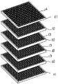
以下、図面を参照して、本発明の実施形態について説明する。図1は誘電体基板を示す斜視図で、使用される誘電体基板は所定の厚みとされ、表面はフォトリソグラフィーが可能な程度に研磨されて平坦化される。図2は複数の誘電体基板を重ねる工程を示す斜視図である。この例では、4素子の誘電体導波管フィルタを構成するもので、4枚の誘電体基板10の表裏面に結合調整用の導体パターン13を形成し、それらの両端に厚みの薄い誘電体基板12を配置して挟むようにしたものである。誘電体基板の表面への導体パターンの形成はフォトリソグラフィー技術を利用できるので、高精度の導体パターンが形成できる。
Embodiments of the present invention will be described below with reference to the drawings. FIG. 1 is a perspective view showing a dielectric substrate. The dielectric substrate used has a predetermined thickness, and the surface is polished and flattened to the extent that photolithography is possible. FIG. 2 is a perspective view showing a process of stacking a plurality of dielectric substrates. In this example, a dielectric waveguide filter having four elements is formed.
4枚の誘電体基板10の表面に形成される導体パターンは、金属膜に縦横に誘電体材料が露出する窓が形成されたパターン13となっている。両端の2枚の薄い誘電体基板11の表面の導体パターンも一部に誘電体が露出したパターンと14なっているが、これは入出力用の導体パターンの端部が誘電体導波管フィルタのアース導体と導通されないようにするためのものである。誘電体基板の厚みや枚数は、フィルタの特性に対応して任意に選択することができる。
The conductor pattern formed on the surface of the four
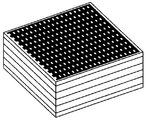
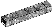
上記のようにして導体パターンが形成された誘電体基板を図3に示したように接合する。接合方法は任意であり、一般的な接着または接合技術を利用すればよい。重ねられて接合された基板を、図4に示したように、切断し、分離する。この工程は水晶振動子の切断等に使用されているマルチワイヤソーなどを用いることができ、切断加工は高精度に一括して行うことができる。切断されて分離されたそれぞれの誘電体ブロック16の端面および内部には図5に示したような導体パターンが形成されていることになる。すなわち、この例では5つの結合調整用パターンが内部に形成され、端面には一部を除いてアース導体となる導体パターンが形成されている。これらの導体パターンは図9に示した導体パターンと同じようになっている。
The dielectric substrates on which the conductor patterns are formed as described above are joined as shown in FIG. A joining method is arbitrary, and a general adhesion or joining technique may be used. The stacked and bonded substrates are cut and separated as shown in FIG. In this step, a multi-wire saw or the like used for cutting a crystal unit can be used, and cutting can be performed collectively with high accuracy. A conductor pattern as shown in FIG. 5 is formed on the end face and inside of each
個々の誘電体ブロックの切断面の一面に入出力用の導体パターンが形成される。この入出力用の導体パターンは図10に示した底面の導体ストリップとして単面に引き出す形状とすればよい。導体ストリップの端部は端面の導体パターンに接続されないように、誘電体が露出した部分に接するように引き出される。残りの3つの切断面には前面に導体膜が形成されて、外観が図6に示したような誘電体導波管フィルタが得られる。 Input / output conductor patterns are formed on one side of the cut surface of each dielectric block. The input / output conductor pattern may be drawn to a single surface as the bottom conductor strip shown in FIG. The end of the conductor strip is drawn out so as to be in contact with the exposed portion of the dielectric so as not to be connected to the conductor pattern on the end face. A conductor film is formed on the front surface of the remaining three cut surfaces, and a dielectric waveguide filter having an appearance as shown in FIG. 6 is obtained.
共振器間の結合調整用の導体パターンは、上記の例では図7(a)のものを挙げたが、その形状は任意に選択することができる。例えば、図7(b)のような単純な形状や、図7(c)のようなH形としてもよい。この開口の位置と大きさで共振器間の結合を調整することができる。 In the above example, the conductor pattern for adjusting the coupling between the resonators is the one shown in FIG. 7A, but the shape thereof can be arbitrarily selected. For example, a simple shape as shown in FIG. 7B or an H shape as shown in FIG. The coupling between the resonators can be adjusted by the position and size of the opening.
本発明による誘電体導波管フィルタの製造方法は、図8に示すように、アイリス共振型フィルタに応用することができる。導波管フィルタにおいては、通常、不連続部で仕切られた半波長または1波長の区間が共振器として動作するように設計される。しかしながら、本発明の生産手法では、導体パターンをミクロンの精度で形成することができるため、導体パターン自体を共振素子として形成し、非常に高い精度で共振周波数を制御することができる。そこで、導体パターンを共振素子としたフィルタを構成することも容易となる。この場合、導体パターン間の距離は管内波長の4分の1程度になり、通常の導波管フィルタは結合パターン間の距離が2分の1となるのに比較して、フィルタ全体の大きさをより小型にすることができる。 The dielectric waveguide filter manufacturing method according to the present invention can be applied to an iris resonant filter as shown in FIG. A waveguide filter is usually designed so that a half-wavelength or one-wavelength section partitioned by discontinuous parts operates as a resonator. However, in the production method of the present invention, since the conductor pattern can be formed with micron accuracy, the conductor pattern itself can be formed as a resonance element, and the resonance frequency can be controlled with very high accuracy. Therefore, it is easy to configure a filter using the conductive pattern as a resonance element. In this case, the distance between the conductor patterns is about one-fourth of the guide wavelength, and a normal waveguide filter has a size of the entire filter as compared with the one-half distance between the coupling patterns. Can be made smaller.
本発明は、マイクロ波帯からミリ波帯に利用できる誘電体導波管フィルタのあらゆる帯域に応用できる。 The present invention can be applied to all bands of dielectric waveguide filters that can be used from the microwave band to the millimeter wave band.
10、11:誘電体基板
13、14:導体パターン
16:誘電体ブロック
10, 11: Dielectric substrate
13, 14: Conductor pattern
16: Dielectric block
Claims (3)
それらの複数の誘電体基板を接合し、
接合された誘電体基板を表面に垂直な方向に切断して内部に導体パターンを具えた複数の誘電体ブロックを形成し、
切断面の1つに入出力用の導体パターンを形成し、当該切断面の入出力用の導体パターンが形成された部分以外のと、その他の3つの切断面の全面に導体膜を形成する誘電体導波管フィルタの製造方法。 Forming a conductor pattern having a coupling window on the joint surface of a plurality of dielectric substrates;
Bond these multiple dielectric substrates,
Cutting the bonded dielectric substrate in a direction perpendicular to the surface to form a plurality of dielectric blocks having a conductor pattern inside,
A dielectric that forms an input / output conductor pattern on one of the cut surfaces and forms a conductor film on the entire surface of the other three cut surfaces other than the portion where the input / output conductor pattern is formed on the cut surface. Method for manufacturing a body waveguide filter.
それらの複数の誘電体基板を接合し、
接合された誘電体基板を表面に垂直な方向に切断して内部に導体パターンを具えた複数の誘電体ブロックを形成し、
切断面の1つに端面まで伸びる入出力用の導体ストリップを形成し、当該切断面の入出力用の導体パターンが形成された部分以外のと、その他の3つの切断面の全面に導体膜を形成する誘電体導波管フィルタの製造方法。 A conductor pattern having a coupling window is formed on the joint surfaces of a plurality of dielectric substrates, and a conductor film is formed on a portion other than the portion in contact with the input / output conductor pattern on the surface other than the joint surface,
Bond these multiple dielectric substrates,
Cutting the bonded dielectric substrate in a direction perpendicular to the surface to form a plurality of dielectric blocks having a conductor pattern inside,
An input / output conductor strip extending to the end face is formed on one of the cut surfaces, and a conductor film is formed on the entire surface of the other three cut surfaces other than the portion where the input / output conductor pattern of the cut surface is formed. A method of manufacturing a dielectric waveguide filter to be formed.
Priority Applications (1)
| Application Number | Priority Date | Filing Date | Title |
|---|---|---|---|
| JP2005163811A JP2006340141A (en) | 2005-06-03 | 2005-06-03 | Manufacturing method of dielectric waveguide filter |
Applications Claiming Priority (1)
| Application Number | Priority Date | Filing Date | Title |
|---|---|---|---|
| JP2005163811A JP2006340141A (en) | 2005-06-03 | 2005-06-03 | Manufacturing method of dielectric waveguide filter |
Publications (1)
| Publication Number | Publication Date |
|---|---|
| JP2006340141A true JP2006340141A (en) | 2006-12-14 |
Family
ID=37560269
Family Applications (1)
| Application Number | Title | Priority Date | Filing Date |
|---|---|---|---|
| JP2005163811A Withdrawn JP2006340141A (en) | 2005-06-03 | 2005-06-03 | Manufacturing method of dielectric waveguide filter |
Country Status (1)
| Country | Link |
|---|---|
| JP (1) | JP2006340141A (en) |
Cited By (4)
| Publication number | Priority date | Publication date | Assignee | Title |
|---|---|---|---|---|
| CN109216842A (en) * | 2017-07-07 | 2019-01-15 | 日本电产株式会社 | The manufacturing method of waveguide assembly |
| JP2019097205A (en) * | 2013-09-23 | 2019-06-20 | シーティーエス・コーポレーションCts Corporation | Dielectric waveguide filter with direct coupling and alternative cross-coupling |
| CN114006144A (en) * | 2021-11-24 | 2022-02-01 | 天津大学 | Method for manufacturing dielectric waveguide radio frequency device |
| US11437691B2 (en) | 2019-06-26 | 2022-09-06 | Cts Corporation | Dielectric waveguide filter with trap resonator |
-
2005
- 2005-06-03 JP JP2005163811A patent/JP2006340141A/en not_active Withdrawn
Cited By (5)
| Publication number | Priority date | Publication date | Assignee | Title |
|---|---|---|---|---|
| JP2019097205A (en) * | 2013-09-23 | 2019-06-20 | シーティーエス・コーポレーションCts Corporation | Dielectric waveguide filter with direct coupling and alternative cross-coupling |
| CN109216842A (en) * | 2017-07-07 | 2019-01-15 | 日本电产株式会社 | The manufacturing method of waveguide assembly |
| US11437691B2 (en) | 2019-06-26 | 2022-09-06 | Cts Corporation | Dielectric waveguide filter with trap resonator |
| CN114006144A (en) * | 2021-11-24 | 2022-02-01 | 天津大学 | Method for manufacturing dielectric waveguide radio frequency device |
| CN114006144B (en) * | 2021-11-24 | 2022-05-03 | 天津大学 | Method for manufacturing dielectric waveguide radio frequency device |
Similar Documents
| Publication | Publication Date | Title |
|---|---|---|
| JP3166897B2 (en) | Non-radiative dielectric line and its integrated circuit | |
| EP0856903B1 (en) | Multiple-mode dielectric resonator and method of adjusting characteristic of the resonator | |
| US7102469B2 (en) | Open loop resonator filter using aperture | |
| JP4021773B2 (en) | Waveguide type dielectric filter and manufacturing method thereof | |
| WO2002005379A1 (en) | Filter | |
| JPH0375081B2 (en) | ||
| MX2015002935A (en) | Band-pass filter. | |
| US6600392B2 (en) | Metal window filter assembly using non-radiative dielectric waveguide | |
| JP2006340141A (en) | Manufacturing method of dielectric waveguide filter | |
| JPH0211163B2 (en) | ||
| JPH07263998A (en) | End face reflecting surface wave resonator | |
| JP2765396B2 (en) | Stripline filter and microstrip line filter | |
| US5291162A (en) | Method of adjusting frequency response in a microwave strip-line filter device | |
| US20020190822A1 (en) | Metal post filter assembly using non-radiative dielectric waveguide | |
| JP2004312287A (en) | Dielectric resonator, dielectric filter, composite dielectric filter, and communication apparatus | |
| JP3812505B2 (en) | Cavity resonator, cavity resonator filter and module substrate | |
| JP2002217602A (en) | Dielectric filter and method for manufacturing the same | |
| JPS58194402A (en) | Dielectric filter | |
| JP2869332B2 (en) | Dielectric filter and method of manufacturing the same | |
| JP2869331B2 (en) | Dielectric filter and method of manufacturing the same | |
| JPH09223904A (en) | Dielectric filter | |
| JP2869329B2 (en) | Dielectric filter and method of manufacturing the same | |
| JPH07283608A (en) | Dielectric filter and its production | |
| JP2869333B2 (en) | Dielectric filter and method of manufacturing the same | |
| KR100446258B1 (en) | Bulk Acoustic Wave Device for High Frequency Using Piezoelectric Single Crystal and Process of The Same |
Legal Events
| Date | Code | Title | Description |
|---|---|---|---|
| A621 | Written request for application examination |
Free format text: JAPANESE INTERMEDIATE CODE: A621 Effective date: 20071220 |
|
| A977 | Report on retrieval |
Free format text: JAPANESE INTERMEDIATE CODE: A971007 Effective date: 20090217 |
|
| A131 | Notification of reasons for refusal |
Free format text: JAPANESE INTERMEDIATE CODE: A131 Effective date: 20090224 |
|
| A761 | Written withdrawal of application |
Free format text: JAPANESE INTERMEDIATE CODE: A761 Effective date: 20090327 |