JP2006324310A - INTEGRAL SiC-CMP DRESSER PAD - Google Patents
INTEGRAL SiC-CMP DRESSER PAD Download PDFInfo
- Publication number
- JP2006324310A JP2006324310A JP2005143921A JP2005143921A JP2006324310A JP 2006324310 A JP2006324310 A JP 2006324310A JP 2005143921 A JP2005143921 A JP 2005143921A JP 2005143921 A JP2005143921 A JP 2005143921A JP 2006324310 A JP2006324310 A JP 2006324310A
- Authority
- JP
- Japan
- Prior art keywords
- pad
- dresser
- polishing
- sic
- abrasive grains
- Prior art date
- Legal status (The legal status is an assumption and is not a legal conclusion. Google has not performed a legal analysis and makes no representation as to the accuracy of the status listed.)
- Pending
Links
- 238000005498 polishing Methods 0.000 claims abstract description 53
- 239000006061 abrasive grain Substances 0.000 claims abstract description 28
- 239000004065 semiconductor Substances 0.000 claims abstract description 8
- PXHVJJICTQNCMI-UHFFFAOYSA-N Nickel Chemical compound [Ni] PXHVJJICTQNCMI-UHFFFAOYSA-N 0.000 description 34
- 229910003460 diamond Inorganic materials 0.000 description 23
- 239000010432 diamond Substances 0.000 description 23
- 229910052759 nickel Inorganic materials 0.000 description 17
- 238000000034 method Methods 0.000 description 14
- 238000005422 blasting Methods 0.000 description 9
- 238000004070 electrodeposition Methods 0.000 description 8
- 239000002245 particle Substances 0.000 description 8
- 239000002002 slurry Substances 0.000 description 8
- 238000005260 corrosion Methods 0.000 description 3
- 230000007797 corrosion Effects 0.000 description 3
- 239000000463 material Substances 0.000 description 3
- 230000002378 acidificating effect Effects 0.000 description 2
- 238000011109 contamination Methods 0.000 description 2
- 230000001771 impaired effect Effects 0.000 description 2
- 230000000873 masking effect Effects 0.000 description 2
- 230000003287 optical effect Effects 0.000 description 2
- 239000002699 waste material Substances 0.000 description 2
- 229910018072 Al 2 O 3 Inorganic materials 0.000 description 1
- 238000010586 diagram Methods 0.000 description 1
- 239000006185 dispersion Substances 0.000 description 1
- 238000009713 electroplating Methods 0.000 description 1
- 238000010828 elution Methods 0.000 description 1
- 238000005516 engineering process Methods 0.000 description 1
- 230000010354 integration Effects 0.000 description 1
- 239000002184 metal Substances 0.000 description 1
- 229910052751 metal Inorganic materials 0.000 description 1
- 238000000206 photolithography Methods 0.000 description 1
- 238000007747 plating Methods 0.000 description 1
- 238000007517 polishing process Methods 0.000 description 1
- 230000003014 reinforcing effect Effects 0.000 description 1
- 238000005507 spraying Methods 0.000 description 1
- 239000000126 substance Substances 0.000 description 1
- 238000009736 wetting Methods 0.000 description 1
Images

Landscapes
- Finish Polishing, Edge Sharpening, And Grinding By Specific Grinding Devices (AREA)
- Mechanical Treatment Of Semiconductor (AREA)
- Grinding-Machine Dressing And Accessory Apparatuses (AREA)
Abstract
Description
本発明は、半導体ウェーハの表面研磨等に用いられる研磨パッドの目立て装置(ドレッサーパッド)に関する。 The present invention relates to a polishing pad dressing device (dresser pad) used for polishing a surface of a semiconductor wafer.
LSIの高集積化は、多層配線化及び配線微細化により達成されている。多層化は表面段差を増大させ、微細化はフォトリソ工程での焦点深度を小さくする。こうした背景のもと、ウェーハ全面の均一な平坦化にはCMP(化学機械研磨)技術は必須となっている半導体プロセスの一つである。 High integration of LSI is achieved by multilayer wiring and wiring miniaturization. Multi-layering increases the surface level difference, and miniaturization reduces the depth of focus in the photolithography process. Against this background, CMP (Chemical Mechanical Polishing) technology is one of the semiconductor processes that is essential for uniform planarization of the entire wafer surface.
CMPは研磨スラリーを用いて半導体ウェーハの表面を研磨するもので、円盤状の定盤にセットされた半導体ウェーハと、ポリッシングパッド(研磨パッド)を相対的に接触、回転させることによって研磨作業を行う。通常このような研磨作業を長時間行っていると、被研磨部材の削屑や研磨スラリー等が研磨パッドの微細な穴に入り込んで目詰りを起こす。また、研磨パッド表面が平坦化されて研磨速度が著しく低下する。 CMP polishes the surface of a semiconductor wafer using a polishing slurry, and performs polishing work by relatively contacting and rotating a semiconductor wafer set on a disk-shaped surface plate and a polishing pad (polishing pad). . Normally, when such a polishing operation is performed for a long time, chips or polishing slurry of the member to be polished enters a fine hole of the polishing pad and clogs. In addition, the polishing pad surface is flattened and the polishing rate is significantly reduced.
この研磨速度の安定化には研磨パッドのドレッシング(目立て)が必須である。一般に、研磨パッド用のドレッサーパッドは、複数のダイヤモンド砥粒と、これらの砥粒を保持する固着層(メッキ層)とを備えている。ダイヤモンド砥粒は、先端部分のみが研磨パッド側に突出した状態で固着層に保持される。従来の研磨パッド用ドレッサーパッドにおいては、一般に粒径が0.2〜0.3mmのダイヤモンド砥粒が使用されている。 To stabilize the polishing rate, dressing (sharpening) of the polishing pad is essential. Generally, a dresser pad for a polishing pad includes a plurality of diamond abrasive grains and a fixing layer (plating layer) that holds the abrasive grains. The diamond abrasive grains are held by the fixing layer with only the tip portion protruding toward the polishing pad. In conventional dresser pads for polishing pads, diamond abrasive grains having a particle size of 0.2 to 0.3 mm are generally used.
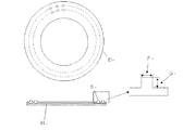
上記のような従来の研磨パッド用ドレッサーパッドにおいて、一般に、ダイヤモンド砥粒の固着にはニッケル電着法が用いられる。図1にニッケル電着法の模式図を示す。ニッケル電着法は、ニッケルの電解メッキに類似した方法であり、ダイヤモンド粒の間の隙間もニッケルで埋めて(図1B)、ダイヤモンド砥粒(図1A)を保持している。しかしながら、ダイヤモンド砥粒とニッケルとの間のぬれはほとんど皆無であり、ダイヤモンド砥粒とニッケルとの間の接合強度は低い。ここで保持できず、脱落してしまったダイヤモンド砥粒はウェーハのスクラッチ傷の原因となる。(図1C:ダイヤモンド砥粒脱落部) In the conventional dresser pad for a polishing pad as described above, generally, a nickel electrodeposition method is used for fixing diamond abrasive grains. FIG. 1 shows a schematic diagram of the nickel electrodeposition method. The nickel electrodeposition method is similar to nickel electroplating, and the gaps between the diamond grains are filled with nickel (FIG. 1B) to hold the diamond abrasive grains (FIG. 1A). However, there is almost no wetting between the diamond abrasive grains and nickel, and the bonding strength between the diamond abrasive grains and nickel is low. The diamond abrasive grains that cannot be held here and fall off cause scratch scratches on the wafer. (FIG. 1C: Diamond abrasive grain dropout part)
さらに、上記のような従来の研磨パッド用ドレッサーパッドにおいては、ダイヤモンド砥粒を無作為に配置しているため、ドレッシングの均一性を向上させるのにも限界があった。また、研磨パッドに対してダイヤモンド砥粒が一様に接触しないと、ドレッシングの均一性が損なわれ、その結果、ウェーハの研磨の均一性が悪化する。 Furthermore, in the conventional dresser pad for a polishing pad as described above, since diamond abrasive grains are randomly arranged, there is a limit to improving the uniformity of dressing. Further, if the diamond abrasive grains do not uniformly contact the polishing pad, the uniformity of the dressing is impaired, and as a result, the uniformity of polishing of the wafer is deteriorated.
さらに、ニッケル電着法を用いる従来の研磨パッド用ドレッサーパッドは、研磨パッド研磨時に研磨パッドに残留したCMPスラリーに対してニッケルの溶出等の問題もある。 Further, the conventional dresser pad for a polishing pad using the nickel electrodeposition method has a problem such as elution of nickel with respect to the CMP slurry remaining on the polishing pad during polishing of the polishing pad.
従って、本発明の目的は、ドレッシング装置におけるドレッサーパッドを一体構造とし、ドレッシングの安定性を向上させることにある。 Accordingly, an object of the present invention is to improve the dressing stability by integrating the dresser pad in the dressing apparatus.
本発明は、半導体ウェーハの研磨に用いられるCMP装置の研磨パッドをドレッシングするドレッシング装置において、従来、複数のダイヤモンド砥粒と、これらの砥粒を保持する固着層とを備えていた研磨パッド用ドレッサーパッドを一体構造型とするものである。このようなドレッサーパッドの一態様としては、一体構造型ドレッサーパッドにはSiCを用い、研磨表面にはダイヤモンド砥粒に代替するSiCピンをブラスト加工を用いて形成したものをあげることができる。 The present invention relates to a dressing device for dressing a polishing pad of a CMP apparatus used for polishing a semiconductor wafer, and conventionally comprising a plurality of diamond abrasive grains and a fixing layer for holding these abrasive grains. The pad is an integral structure type. As one aspect of such a dresser pad, there can be mentioned one in which SiC is used for the monolithic dresser pad, and a SiC pin that replaces diamond abrasive grains is formed on the polishing surface by blasting.
本発明における一体構造型SiC−CMPドレッサーパッドは、従来のダイヤモンド砥粒に代替するピンをブラスト加工によって一体型として形成するため、従来問題であったダイヤモンド砥粒の脱落のような、ピンの脱落などはない。さらに、ピンはブラスト加工によって形成するため、規則的かつ正確に配置できる。無作為にしか配置できなかったダイヤモンド砥粒を用いた従来の研磨パッド用ドレッサーパッドとは違い、研磨パッドを均一にドレスすることが可能となる。 Since the monolithic SiC-CMP dresser pad according to the present invention forms a pin that replaces the conventional diamond abrasive grains as an integral type by blasting, the pin omission such as the omission of diamond abrasive grains, which has been a problem in the past, There is no such thing. Further, since the pins are formed by blasting, they can be arranged regularly and accurately. Unlike a conventional polishing pad dresser pad using diamond abrasive grains that could only be randomly arranged, the polishing pad can be dressed uniformly.
また、ニッケル電着法を用いた従来ドレッサーパッドは、ダイヤモンド砥粒を固着するニッケルがCMPスラリーに溶出し、ウェーハを汚染するのに対して、SiCは金属成分を含有せず、ウェーハの汚染はない。 Also, in the conventional dresser pad using the nickel electrodeposition method, nickel fixing diamond abrasive grains is eluted into the CMP slurry and contaminates the wafer, whereas SiC does not contain a metal component, and the contamination of the wafer is Absent.
本発明は以下の実施の形態を図面を用いて説明するが、本発明はここで説明する実施の形態に限定されるものではない。下記実施の形態は発明の目的を逸脱しない限りにおいて多様に変形することができる。 The following embodiments of the present invention will be described with reference to the drawings, but the present invention is not limited to the embodiments described herein. The following embodiments can be variously modified without departing from the object of the invention.
図2に、本発明におけるSiCドレッサーパッドの概略図を示す。図2に示すように、本発明のSiCドレッサーパッドは円盤状のドレッサーパッドDにSiCピンEを複数個(図では簡単のため6点のみ記載してある)形成した構造になっている。ピンの形成方法は、まず、SiC焼結体のドレッサー面とする面に対して、平面研磨加工を行う。次にブラスト加工を行い、SiCピンを形成する。 In FIG. 2, the schematic of the SiC dresser pad in this invention is shown. As shown in FIG. 2, the SiC dresser pad of the present invention has a structure in which a plurality of SiC pins E (only six points are shown for simplicity) are formed on a disk-shaped dresser pad D. As a method for forming the pins, first, a surface polishing process is performed on the surface of the SiC sintered body as a dresser surface. Next, blasting is performed to form SiC pins.
ブラスト加工は、被加工物に対して研磨粒子を高圧で噴射して研磨する方法で、研磨しない箇所にはマスキングを施すことで多様なパターンを形成することができる。 Blasting is a method in which abrasive particles are sprayed onto a workpiece at a high pressure for polishing, and various patterns can be formed by masking portions that are not polished.
以下に上記ブラスト加工の一例を説明する。まず、平面研磨加工を施した面に、直径φ0.2mm、同心円状、等間隔のマスクパターンを形成した。マスキングはマスクの直径、パターンとも自在に選択可能である。マスクパターン形成には露光法を用いる。露光法は、紫外線によって感光するフィルムを被加工物に貼り、パターンを形成したマスクを重ね合わせ、フィルムに感光させる。感光後、被加工物を現像液中に浸漬することによってネガフィルムによって感光しなかった箇所はブラストマスクとして被加工物に形成される。 An example of the blasting will be described below. First, a mask pattern having a diameter of 0.2 mm, concentric circles, and equal intervals was formed on the surface subjected to the surface polishing. Masking can be freely selected with respect to the mask diameter and pattern. An exposure method is used for forming the mask pattern. In the exposure method, a film that is exposed to ultraviolet rays is attached to a workpiece, a mask on which a pattern is formed is superimposed, and the film is exposed to light. After the exposure, the portion that is not exposed to light by the negative film is immersed in the developer by forming a blast mask on the workpiece.
次に、前記マスクパターンを形成したSiC焼結体のドレッサー面とする面に対して、ブラスト加工を行う。研磨粒子にはSiC粒子を用い、前記面に噴射することでマスクパターンの形成、すなわち、直径φ0.2mm、高さ0.05mmのSiCピンの形成ができる。ピン寸法は、研磨粒子、加工圧力、加工時間、加工回数を変更することで調整することができる。たとえば研磨粒子径を小さくすればピン寸法はより精度の高いものが形成でき、加工圧力を高くすれば高いピンを形成することができる傾向がある。 Next, blasting is performed on the surface of the SiC sintered body on which the mask pattern is formed as a dresser surface. By using SiC particles as the abrasive particles and spraying onto the surface, a mask pattern can be formed, that is, an SiC pin having a diameter of 0.2 mm and a height of 0.05 mm can be formed. The pin size can be adjusted by changing abrasive particles, processing pressure, processing time, and number of processing. For example, if the abrasive particle diameter is reduced, a pin with a higher accuracy can be formed, and if the processing pressure is increased, a higher pin tends to be formed.
従来のニッケル電着法を用いたドレッサーパッドでは、ダイヤモンド砥粒のバラツキの及び、ニッケルによる固着のため、ドレッサー面が研磨パッドに均一に接触せず、ドレッシングの均一性が損なわれてしまう。 In a dresser pad using a conventional nickel electrodeposition method, the dresser surface is not uniformly in contact with the polishing pad due to the dispersion of diamond abrasive grains and the fixation by nickel, and the dressing uniformity is impaired.
これに対して、本発明によるドレッサーパッドは、ドレッサー面のSiCピンの研磨面は、平面研磨によって形成されており、研磨パッドへの接触の均一性は高い。加えて、SiCピンの直径、高さとも均一に形成することができる。 On the other hand, in the dresser pad according to the present invention, the polishing surface of the SiC pin on the dresser surface is formed by flat polishing, and the uniformity of contact with the polishing pad is high. In addition, the diameter and height of the SiC pin can be formed uniformly.
さらに、従来のドレッサーパッドではドレッサー面のダイヤモンド砥粒の配置は無作為であったのに対し、本発明によるドレッサーパッドのSiCピンは規則的かつ精密に配置することができる。 Further, in the conventional dresser pad, the arrangement of the diamond abrasive grains on the dresser surface is random, whereas the SiC pins of the dresser pad according to the present invention can be arranged regularly and precisely.
次に、本発明のドレッサーパッドの一実施態様についてさらに詳しく説明する。まずピン部分の大きさ(以下ピン径という)としては、半導体ウェーハ用研磨パッド用という点でφ0.1〜0.3mmが好ましく、ピンの研磨パッドとの接触面積とピンの数の最適条件からφ0.1〜0.2mmがより好ましい。なお、本発明においてピン径とは、ドレッサーパッドを光学顕微鏡で観察したときの写真から、図2においてFで表される部分を測定することで定義する。 Next, one embodiment of the dresser pad of the present invention will be described in more detail. First, the size of the pin portion (hereinafter referred to as the pin diameter) is preferably 0.1 to 0.3 mm in terms of a semiconductor wafer polishing pad. From the optimum conditions of the contact area of the pins with the polishing pad and the number of pins φ0.1 to 0.2 mm is more preferable. In the present invention, the pin diameter is defined by measuring a portion represented by F in FIG. 2 from a photograph when the dresser pad is observed with an optical microscope.
次にピン部分の高さについては、研磨パッドのドレッシング能力とピン強度の点で0.05〜0.1mmが好ましい。ピン高さが高すぎると、研磨パッド研磨時に、強度不足となりピンが破損してしまう。なお、本発明においてピン高さとは、ドレッサーパッドを光学顕微鏡で観察したときの写真から、図2においてGで表される部分を測定することで定義する。 Next, the height of the pin portion is preferably 0.05 to 0.1 mm in terms of dressing ability of the polishing pad and pin strength. If the pin height is too high, the strength will be insufficient during polishing of the polishing pad and the pin will be damaged. In the present invention, the pin height is defined by measuring a portion represented by G in FIG. 2 from a photograph when the dresser pad is observed with an optical microscope.
次にドレッサーパッドの形状については、ウェーハ研磨に使用する研磨パッドサイズに依存し、外径φ80〜120mm、内径φ50〜60mm、厚み2〜10mmが好ましい。また、研磨時に回転することと、研磨屑が発生することとから、研磨屑を逃がすため、円盤リング状が好ましい。 Next, the shape of the dresser pad is preferably an outer diameter φ80 to 120 mm, an inner diameter φ50 to 60 mm, and a thickness 2 to 10 mm, depending on the size of the polishing pad used for wafer polishing. Moreover, since it rotates at the time of grinding | polishing and a grinding | polishing waste generate | occur | produces, in order to escape grinding | polishing waste, a disk ring shape is preferable.
本発明のドレッサーパッドの材質としては、CMPスラリーに耐食性のある材料、ある程度の強度、硬度、耐摩耗性を有する材料を選択することが好ましく、具体的にはたとえば、SiC、Si3N4、Al2O3、ZrO2、SUS、WCなどをあげることができる。中でも、SiC、Si3N4が好ましく、特にSiCが好ましい。 As the material of the dresser pad of the present invention, it is preferable to select a material having corrosion resistance for the CMP slurry, and a material having a certain degree of strength, hardness, and wear resistance. Specifically, for example, SiC, Si 3 N 4 , Al 2 O 3 , ZrO 2 , SUS, WC and the like can be mentioned. Among these, SiC and Si 3 N 4 are preferable, and SiC is particularly preferable.
なお本発明のドレッサーパッドの一態様として、図2Hに示すように、ドレッサーパッド部の下に補強部材を設けた構造であってもよい。 As an aspect of the dresser pad of the present invention, as shown in FIG. 2H, a structure in which a reinforcing member is provided below the dresser pad portion may be used.
以下、実施例により本発明を説明するが、本発明はこれに制限されるものではない。
実施例1
外径φ100mm、内径φ60mm、厚さ2mmのSiC焼結体リングの表面に平面研磨加工を施した後、ブラスト加工によって、高さ0.05mmのピンを同心円上に形成し一体構造型SiC―CMPドレッサーパッドを得た。露光条件は露光量350mJ/cm2である。ブラスト加工条件は、研磨粒子SiC粒子(#220)、加工圧力0.34MPaである。
EXAMPLES Hereinafter, although an Example demonstrates this invention, this invention is not restrict | limited to this.
Example 1
The surface of the SiC sintered body ring having an outer diameter of φ100 mm, an inner diameter of φ60 mm, and a thickness of 2 mm is subjected to surface polishing, and then a pin having a height of 0.05 mm is formed on a concentric circle by blasting, so that the monolithic SiC-CMP A dresser pad was obtained. The exposure condition is an exposure amount of 350 mJ / cm 2 . The blasting conditions are abrasive particles SiC particles (# 220) and a processing pressure of 0.34 MPa.
次に上記、一体構造型SiC−CMPドレッサーパッドの研磨後の面状態について評価した。 Next, the surface state after polishing of the monolithic SiC-CMP dresser pad was evaluated.
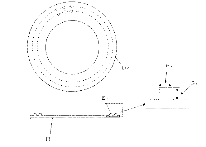
表1に示されるように、本発明による一体構造型SiC−CMPドレッサーパッドは、従来のニッケル電着法を用いたドレッサーパッドのようなダイヤモンド砥粒の脱落、といった問題はなく、かつ、SiCピン径、ピン高さも自由に選択・制御可能であり、研磨の安定性が向上する。 As shown in Table 1, the monolithic SiC-CMP dresser pad according to the present invention has no problem of dropping diamond abrasive grains like a conventional dresser pad using a nickel electrodeposition method. The diameter and pin height can also be freely selected and controlled, improving the stability of polishing.
次に上記、一体構造型SiC−CMPドレッサーパッドの耐食性について評価した。 Next, the corrosion resistance of the monolithic SiC-CMP dresser pad was evaluated.
表2に示されるように、本発明による一体構造型SiC−CMPドレッサーパッドは、アルカリスラリー、及び酸性スラリーに対しても不溶であり、極めて耐食性が高くウェーハへの汚染がないことがわかる。これに対して従来のニッケル電着法を用いたドレッサーパッドは、酸性スラリーに対してニッケル成分を溶出した。 As shown in Table 2, it can be seen that the monolithic SiC-CMP dresser pad according to the present invention is insoluble in alkaline slurry and acidic slurry, and has extremely high corrosion resistance and no contamination to the wafer. On the other hand, the dresser pad using the conventional nickel electrodeposition method eluted the nickel component with respect to the acidic slurry.
A・・・ダイヤモンド砥粒
B・・・ニッケル層
C・・・ダイヤモンド砥粒脱落箇所
D・・・ドレッサーパッド
E・・・SiCピン
F・・・ピン径
G・・・ピン高さ
A ... Diamond abrasive grain B ... Nickel layer C ... Diamond abrasive grain drop-off point D ... Dresser pad E ... SiC pin F ... Pin diameter G ... Pin height
Claims (2)
2. The monolithic SiC-CMP dresser pad according to claim 1, comprising a SiC sintered body.
Priority Applications (1)
| Application Number | Priority Date | Filing Date | Title |
|---|---|---|---|
| JP2005143921A JP2006324310A (en) | 2005-05-17 | 2005-05-17 | INTEGRAL SiC-CMP DRESSER PAD |
Applications Claiming Priority (1)
| Application Number | Priority Date | Filing Date | Title |
|---|---|---|---|
| JP2005143921A JP2006324310A (en) | 2005-05-17 | 2005-05-17 | INTEGRAL SiC-CMP DRESSER PAD |
Publications (1)
| Publication Number | Publication Date |
|---|---|
| JP2006324310A true JP2006324310A (en) | 2006-11-30 |
Family
ID=37543790
Family Applications (1)
| Application Number | Title | Priority Date | Filing Date |
|---|---|---|---|
| JP2005143921A Pending JP2006324310A (en) | 2005-05-17 | 2005-05-17 | INTEGRAL SiC-CMP DRESSER PAD |
Country Status (1)
| Country | Link |
|---|---|
| JP (1) | JP2006324310A (en) |
Cited By (2)
| Publication number | Priority date | Publication date | Assignee | Title |
|---|---|---|---|---|
| JP2008183659A (en) * | 2007-01-30 | 2008-08-14 | Disco Abrasive Syst Ltd | Grinding equipment |
| US11583975B2 (en) | 2019-03-08 | 2023-02-21 | Kioxia Corporation | Dresser, polishing device, and method of dressing polishing pad |
Citations (3)
| Publication number | Priority date | Publication date | Assignee | Title |
|---|---|---|---|---|
| JPH10138120A (en) * | 1996-10-31 | 1998-05-26 | Kyocera Corp | Dressing jig |
| JP2003053665A (en) * | 2001-08-10 | 2003-02-26 | Mitsubishi Materials Corp | dresser |
| JP2004291129A (en) * | 2003-03-26 | 2004-10-21 | Mitsubishi Materials Corp | Soft material processing tool |
-
2005
- 2005-05-17 JP JP2005143921A patent/JP2006324310A/en active Pending
Patent Citations (3)
| Publication number | Priority date | Publication date | Assignee | Title |
|---|---|---|---|---|
| JPH10138120A (en) * | 1996-10-31 | 1998-05-26 | Kyocera Corp | Dressing jig |
| JP2003053665A (en) * | 2001-08-10 | 2003-02-26 | Mitsubishi Materials Corp | dresser |
| JP2004291129A (en) * | 2003-03-26 | 2004-10-21 | Mitsubishi Materials Corp | Soft material processing tool |
Cited By (2)
| Publication number | Priority date | Publication date | Assignee | Title |
|---|---|---|---|---|
| JP2008183659A (en) * | 2007-01-30 | 2008-08-14 | Disco Abrasive Syst Ltd | Grinding equipment |
| US11583975B2 (en) | 2019-03-08 | 2023-02-21 | Kioxia Corporation | Dresser, polishing device, and method of dressing polishing pad |
Similar Documents
| Publication | Publication Date | Title |
|---|---|---|
| JP2896657B2 (en) | Dresser and manufacturing method thereof | |
| CN107206567B (en) | Wafer Pin Chuck Manufacturing and Repair | |
| JP3527448B2 (en) | Dresser for CMP polishing cloth and its manufacturing method | |
| US6540597B1 (en) | Polishing pad conditioner | |
| JP2009260142A (en) | Wafer-polishing apparatus and wafer-polishing method | |
| TWI898132B (en) | Processing methods | |
| CN110091265B (en) | Method for manufacturing polishing pad conditioner by reverse plating and polishing pad conditioner manufactured thereby | |
| US9505166B2 (en) | Rectangular mold-forming substrate | |
| CN113400176A (en) | Silicon wafer edge polishing device and method | |
| JPH08139169A (en) | Method for manufacturing ceramic member for wafer holding table | |
| TW201524686A (en) | Dressing method and dressing device | |
| KR100645748B1 (en) | Diamond tool manufacturing method and diamond tool using the same | |
| JP2006324310A (en) | INTEGRAL SiC-CMP DRESSER PAD | |
| JPH09232257A (en) | Polishing method | |
| JP4624293B2 (en) | CMP pad conditioner | |
| JP2007118120A (en) | Polishing method and device | |
| JPH1177535A (en) | Conditioner and method of manufacturing the same | |
| JP2000141204A (en) | Dressing apparatus, polishing apparatus and CMP apparatus using the same | |
| TW202436029A (en) | Repair components | |
| JP2003071717A (en) | Polishing pad adjusting tool | |
| JP2003080457A (en) | Cutting tool and manufacturing method therefor | |
| WO2008082056A1 (en) | Diamond tool and method for manufacturing the same | |
| JP2005254343A (en) | Notch wheel | |
| KR200303718Y1 (en) | CMP pad conditioner | |
| JP2000190199A (en) | Plane correcting method for surface plate |
Legal Events
| Date | Code | Title | Description |
|---|---|---|---|
| A621 | Written request for application examination |
Free format text: JAPANESE INTERMEDIATE CODE: A621 Effective date: 20080430 |
|
| A977 | Report on retrieval |
Free format text: JAPANESE INTERMEDIATE CODE: A971007 Effective date: 20101203 |
|
| A131 | Notification of reasons for refusal |
Free format text: JAPANESE INTERMEDIATE CODE: A131 Effective date: 20101209 |
|
| A02 | Decision of refusal |
Free format text: JAPANESE INTERMEDIATE CODE: A02 Effective date: 20110331 |