JP2006295142A - Piezoelectric element - Google Patents
Piezoelectric element Download PDFInfo
- Publication number
- JP2006295142A JP2006295142A JP2006068779A JP2006068779A JP2006295142A JP 2006295142 A JP2006295142 A JP 2006295142A JP 2006068779 A JP2006068779 A JP 2006068779A JP 2006068779 A JP2006068779 A JP 2006068779A JP 2006295142 A JP2006295142 A JP 2006295142A
- Authority
- JP
- Japan
- Prior art keywords
- layer
- thin film
- piezoelectric element
- piezoelectric
- electrode layer
- Prior art date
- Legal status (The legal status is an assumption and is not a legal conclusion. Google has not performed a legal analysis and makes no representation as to the accuracy of the status listed.)
- Pending
Links
Images


Abstract
Description
本発明は例えばセンサ、アクチュエータなどに用いられる圧電薄膜を用いた圧電素子に関するものである。 The present invention relates to a piezoelectric element using a piezoelectric thin film used for, for example, a sensor or an actuator.
ペロブスカイト型構造を有する強誘電体の圧電薄膜は優れた誘電性・圧電性・焦電性を有しており、各種センサ、アクチュエータ、トランスデューサなど幅広い圧電デバイスへの応用が期待されている。 A ferroelectric piezoelectric thin film having a perovskite structure has excellent dielectric properties, piezoelectric properties, and pyroelectric properties, and is expected to be applied to various piezoelectric devices such as various sensors, actuators, and transducers.
圧電体は内部に自発分極を有しており、これに外圧が加わるとそのひずみによって分極電荷に変化が生じ、電流が発生する。逆に、圧電体に電圧を印加するとそれに応じて圧電体は伸縮する。 The piezoelectric body has spontaneous polarization inside. When an external pressure is applied to the piezoelectric body, the polarization charge is changed by the distortion, and a current is generated. Conversely, when a voltage is applied to the piezoelectric body, the piezoelectric body expands and contracts accordingly.
このような圧電体を薄膜技術にて形成した圧電素子は基板の上に下部電極層、圧電薄膜層および上部電極層を順次積層形成することにより構成することができ、この下部電極層と上部電極層との間に電圧を印加すると圧電薄膜層は伸縮し、機械的変位が得られるものである。 A piezoelectric element in which such a piezoelectric body is formed by thin film technology can be configured by sequentially laminating a lower electrode layer, a piezoelectric thin film layer, and an upper electrode layer on a substrate. When a voltage is applied between the layers, the piezoelectric thin film layer expands and contracts, and mechanical displacement is obtained.
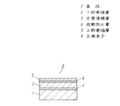
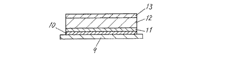
このような圧電薄膜による圧電素子の構造としては図7に示すようなものがある。図7は従来の圧電素子の構造を示す断面図であり、その構造はシリコン基板の上に、熱酸化もしくはCVD法により形成されたSiO2からなる振動板9を形成した後、スパッタ法もしくは蒸着法で形成された密着層(Ti)10および下部電極層(Pt)11、ゾルゲル法により形成された圧電薄膜層(PZT)12、電子ビーム蒸着法もしくはスパッタ法で形成された上部電極層13とからなっている。
A structure of a piezoelectric element using such a piezoelectric thin film is as shown in FIG. FIG. 7 is a cross-sectional view showing the structure of a conventional piezoelectric element. In the structure, a diaphragm 9 made of SiO 2 formed by thermal oxidation or CVD is formed on a silicon substrate, and then sputtering or vapor deposition is performed. An adhesion layer (Ti) 10 and a lower electrode layer (Pt) 11 formed by a method, a piezoelectric thin film layer (PZT) 12 formed by a sol-gel method, an
このとき、密着層(Ti)10は振動板9と下部電極層11との密着力を高める観点から設けられているものである。
At this time, the adhesion layer (Ti) 10 is provided from the viewpoint of increasing the adhesion between the diaphragm 9 and the
そして、この密着層10および下部電極層11には、PZTを結晶化するための焼成工程において、印加される熱によって密着層10を構成するTiが圧電薄膜層(PZT)12中に拡散することを防止するためにPbを含有させている(例えば、特許文献1参照)。
しかしながら、前記従来の構成では、圧電薄膜層12の焼成工程における圧電薄膜層12と下部電極層11および密着層10との拡散のみしか考慮されておらず、焼成工程の後、特に上部電極層13を形成した後に印加される熱や電界等の負荷に関しては考慮されていない。例えば、圧電素子を自動車のエンジンルーム内の高温下で使用した場合、上部電極層13を構成する原子の圧電薄膜層12への拡散および圧電薄膜層12を構成する原子の上部電極層13への拡散などによって、圧電薄膜層12に電流リークが発生するという問題点を有していた。この理由として、例えば圧電薄膜層12にPb(Zr1-xTix)O3(PZT)を用いたとき、拡散反応によってPZT中の酸素原子が欠損すると、PZT中にPb過剰領域ができることによって電流のリークパスができるものと考えられる。あるいは、PbリッチのPZTはPbが結晶粒界にPbOとして偏析しており、その酸素原子が拡散すると結晶粒界に残ったPbがリークパスになるものとも考えられる。
However, in the conventional configuration, only diffusion of the piezoelectric
本発明は、前記従来の課題を解決するものであり、熱や電界等の負荷での圧電素子の上部電極層と圧電薄膜層との間で生じる拡散等の反応を抑制し、熱や電界が印加された状態においても信頼性に優れた圧電薄膜からなる圧電素子を提供することを目的とする。 The present invention solves the above-described conventional problems, suppresses reactions such as diffusion between the upper electrode layer of the piezoelectric element and the piezoelectric thin film layer under a load such as heat and electric field, and generates heat and electric field. An object of the present invention is to provide a piezoelectric element composed of a piezoelectric thin film having excellent reliability even in an applied state.
前記従来の課題を解決するために、本発明は、基板の一面に下部電極層、圧電薄膜層および上部電極層を順次積層して形成した圧電素子において、上部電極層と圧電薄膜層との間に拡散防止層を設けた構成とするものである。 In order to solve the above-described conventional problems, the present invention provides a piezoelectric element formed by sequentially laminating a lower electrode layer, a piezoelectric thin film layer, and an upper electrode layer on one surface of a substrate, and between the upper electrode layer and the piezoelectric thin film layer. It is set as the structure which provided the diffusion prevention layer.
本発明の圧電素子は熱や電界等の負荷による圧電薄膜層と上部電極層との間で生じる拡散反応を抑制することができることから、大きな負荷のかかる環境下においても安定した特性を発揮することができる圧電素子を提供することができる。 Since the piezoelectric element of the present invention can suppress a diffusion reaction that occurs between the piezoelectric thin film layer and the upper electrode layer due to a load such as heat or an electric field, it exhibits stable characteristics even under a heavy load environment. It is possible to provide a piezoelectric element capable of
(実施の形態1)
以下、本発明の実施の形態1における圧電素子について、図面を参照しながら説明する。
(Embodiment 1)
Hereinafter, the piezoelectric element according to the first embodiment of the present invention will be described with reference to the drawings.
図1は本発明の実施の形態1における圧電素子の構造を説明するための断面図、図2〜図5は本発明の実施の形態1における圧電素子の製造工程を説明するための断面図である。 FIG. 1 is a cross-sectional view for explaining the structure of the piezoelectric element according to the first embodiment of the present invention, and FIGS. 2 to 5 are cross-sectional views for explaining the manufacturing process of the piezoelectric element according to the first embodiment of the present invention. is there.
図1において、本実施の形態1における圧電素子8は、シリコンなどの基板1の上にTiとPt薄膜を積層することによって下部電極層2を形成し、その上に圧電性に優れたPb(Zr1-xTix)O3薄膜などの圧電薄膜層3を形成している。この下部電極層2を形成する際には、基板1と下部電極層2の密着力を確保することが圧電素子の信頼性の観点から重要であり、そのために基板1と下部電極層2に対して親和性のあるTiなどの材料を用いて形成することが好ましく、さらに前記親和性のある材料とAu、Ptなどの低抵抗の金属材料を積層して形成することで密着力を確保することも効果的である。
In FIG. 1, a piezoelectric element 8 according to the first embodiment forms a
また、圧電薄膜層3としてはPZT膜が圧電特性の観点からより好ましく、このPZT膜からなる圧電薄膜層3の結晶を(001)に配向させることによって圧電特性をより高めることが可能である。
The piezoelectric
次に、前記圧電薄膜層3の上に拡散防止層4を形成している。この拡散防止層4は圧電薄膜層3と結晶粒径あるいは格子定数などが異なるペロブスカイト型結晶構造を有する誘電体酸化物が好ましい。また、このときの拡散防止層4の厚みとしては300〜2000Åが好ましい。
Next, a
次に、この拡散防止層4の上にTiとAu薄膜を積層することによって上部電極層5を構成している。この上部電極層5を形成する際、上部電極層5と圧電薄膜層3の密着力を確保することが圧電素子の信頼性の観点から重要であり、そのために上部電極層5と圧電薄膜層3に対して親和性のあるTiなどの材料を用いて形成することが好ましく、さらに前記親和性のある材料とAu、Ptなどの低抵抗率の材料を積層して形成することで密着力を確保することも効果的である。このような上部電極層5と圧電薄膜層3に対して親和性のあるTiと同様の効果を発揮する金属としてはCr、Al、Cuなどの金属がある。
Next, the
このような構成を有する圧電素子の圧電薄膜層3と拡散防止層4の結晶粒界は、その断面方向において不連続性を実現しておくことが重要であり、さらにこの拡散防止層4には圧電素子の電気特性を阻害するような材料は好ましくない。例えば、SiO2、Al2O3などの誘電体酸化物は拡散防止には効果があることが分かったが、このような酸化物を拡散防止層4に用いて作製した圧電素子は十分な圧電特性を示さないことが分かった。特に圧電薄膜層3と比べて拡散防止層4の誘電率が低いと、圧電素子を駆動するために印加した電圧は圧電薄膜層3に印加されずに拡散防止層4にその大半が印加されてしまうことになる。このような電気特性への弊害を防止するために拡散防止層4の構成材料について検討した結果、ABO3ペロブスカイト構造を有する誘電体酸化物が好ましいことが分かった。このABO3ペロブスカイト構造は単位格子の8つの頂点位置にAイオンが、体心位置にBイオンが、面心位置にOイオンが位置したものである。このような結晶構造を有する誘電体酸化物のc軸方向に電界を印加すると、BイオンとOイオンが相対的に逆方向に変位し、この電荷の相対的な偏位によって分極を生じる。このABO3型の誘電体酸化物としてはBaTiO3、Pb1-xLaxTiO3などがあり、SiO2、Al2O3などの誘電体酸化物に対して誘電率が比較的高い材料である。このペロブスカイト型構造を有する誘電体酸化物について、どの程度の誘電率が必要であるかについては圧電薄膜層3の誘電特性と拡散防止層4の誘電特性を加味するとともに圧電素子の等価回路定数に基づいて最適な回路定数になるように設計することが可能である。
It is important that the crystal grain boundaries of the piezoelectric
圧電薄膜層3と拡散防止層4の結晶の不連続性を実現するためには圧電薄膜層3と格子定数、原子間距離の異なるペロブスカイト構造を有する誘電体酸化物を拡散防止層4に用いることが有効である。
In order to realize crystal discontinuity between the piezoelectric
また、スパッタ法で形成した(001)配向したPZTからなる圧電薄膜層3の上にスパッタ法とは異なる、例えばCVD法あるいはゾルゲル法などを用いて誘電体酸化物を形成することによって圧電薄膜層3と拡散防止層4との間に結晶の不連続性を有した薄膜積層構造を実現することができる。このような結晶の不連続性を持たせることによって、圧電薄膜層3の結晶粒界に上部電極層5を構成するTiが拡散したり、圧電薄膜層3の結晶粒界近傍の酸素原子が上部電極層5へ拡散することを防止することができるものである。
Also, a piezoelectric thin film layer is formed by forming a dielectric oxide on the piezoelectric
さらに、このような圧電薄膜層3にPb(Zr1-xTix)O3を形成したとき、このPb(Zr1-xTix)O3層と拡散防止層4との結晶界面において、結晶の不連続性を実現することができる材料としては、Mg添加のPb1-xLaxTiO3、無配向のPb(Zr1-xTix)O3などの誘電体酸化物が挙げられ、このような材料を拡散防止層4として用いることで、熱や電界等の負荷下における圧電素子の上部電極層5と圧電薄膜層3との間で生じる拡散等の反応をより抑制できるとともに、電気特性の安定した圧電薄膜からなる圧電素子8を実現することができる。
Further, when Pb (Zr 1-x Ti x ) O 3 is formed on such a piezoelectric
その結果、このような構成を有する圧電素子8を例えば自動車のエンジンルーム内の高温下で使用した場合、上部電極層5を構成する原子の圧電薄膜層3の結晶粒界への拡散および圧電薄膜層3を構成する原子の上部電極層5への拡散移動を抑制することができることから、圧電薄膜層3で発生するリーク電流を抑制できる圧電素子8を実現することができる。
As a result, when the piezoelectric element 8 having such a configuration is used at a high temperature in an engine room of an automobile, for example, diffusion of atoms constituting the
次に、このような構成を有する圧電素子8の製造方法について図面を用いて説明する。 Next, a method for manufacturing the piezoelectric element 8 having such a configuration will be described with reference to the drawings.
まず、図2に示すように厚みが500μmのシリコンからなる基板1の上に、基板1とその上に形成する圧電薄膜層3と親和性を有する材料としてTiを100〜200Åの厚みで形成し、その上にPtを4000〜5000Åの厚みで積層することによって下部電極層2を形成する。この下部電極層2を形成する方法としてはDCまたはRFマグネトロンスパッタリング等の方法が代表的である。
First, as shown in FIG. 2, on a
次に、図3に示すようにPb(Zr1-xTix)O3をスパッタリング等の方法により2〜3μmの厚みで圧電薄膜層3として形成する。(001)に配向したPb(Zr1-xTix)O3は高い圧電性を有することから、電気特性に優れた圧電素子8を実現することができる。
Next, as shown in FIG. 3, Pb (Zr 1-x Ti x ) O 3 is formed as a piezoelectric
次に、図4に示すように、Mg添加のPb1-xLaxTiO3膜を300〜2000Åの厚みで拡散防止層4として圧電薄膜層3の上に形成する。この拡散防止層4に用いることができる材料としては圧電薄膜層3の結晶粒を核生成サイトとすることなく形成することができるペロブスカイト型構造を有する誘電体酸化物であることが好ましい。さらに、拡散防止層4の誘電体酸化物の結晶は圧電薄膜層3の結晶とは異なる位置もしくは異なる結晶サイズで成長させておくことが重要であり、その断面方向において不連続となるように形成している。
Next, as shown in FIG. 4, an Mg-added Pb 1-x La x TiO 3 film is formed on the piezoelectric
また、この拡散防止層4を無配向のペロブスカイト型の誘電体酸化物とした場合、その結晶は配向した圧電薄膜層3の結晶とは異なることから、拡散防止層4と圧電薄膜層3の結晶粒界はその断面方向において不連続とすることができる。圧電薄膜層3を配向したPb(Zr1-xTix)O3として形成したとき、拡散防止層4を無配向性結晶構造のPb(Zr1-xTix)O3を形成することが圧電特性、親和性の観点からより好ましい。このような構成を有する積層膜は薄膜形成プロセスを異ならせることによって実現することができる。
Further, when the
例えば、配向性を有するPb(Zr1-xTix)O3膜をスパッタ法で形成し、その上にCVD法あるいはゾルゲル法で無配向のPb(Zr1-xTix)O3膜を形成することによって作製することができる。
For example, a Pb (Zr 1-x Ti x) O 3 film having orientation is formed by sputtering, a non-oriented by a CVD method or a sol-gel method on the Pb a (Zr 1-x Ti x)
次に、図5に示すように上部電極層5として、例えば下地にCrやTi等、酸化物と親和性を有する金属を50〜200Åの厚みで薄く形成し、その後Au等をスパッタリング、真空蒸着法の方法により2000〜4000Åの厚みで形成することによって密着強度に優れた上部電極層5を形成することができる。
Next, as shown in FIG. 5, as the
その後、この積層した薄膜をウェットエッチングまたはドライエッチングで目的の圧電素子の形状に加工することによってそれぞれの圧電素子8を作製することができる。 Thereafter, the laminated thin film is processed into the shape of the target piezoelectric element by wet etching or dry etching, whereby each piezoelectric element 8 can be manufactured.
このような積層構造を有する圧電素子8(実施例)と、圧電薄膜層3と上部電極層5との間に拡散防止層4を形成していない圧電素子(従来例)に熱ストレスおよび電界ストレスを印加し、その時に生じるリーク電流の経時変化をモニタすることで、拡散防止層4の効果を評価した。評価には電極パターンを1cm×1cmの形状に形成した圧電素子を試料として用いた。加速試験として、これらの試料をホットプレート上で170℃まで加熱し、その状態で上部電極層5と下部電極層2に10V/μmの電界を印加し、そのときの圧電素子のリーク電流量を測定した。
Thermal stress and electric field stress are applied to the piezoelectric element 8 (Example) having such a laminated structure and the piezoelectric element (conventional example) in which the
その結果、拡散防止層4を形成していない従来の圧電素子(従来例)は10秒以下でリーク電流が発生するのに対して、拡散防止層4を導入した圧電素子8(実施例)は10000秒以上の時間が経過してもリーク電流は発生せず、優れた信頼性を有する圧電素子を実現していることが確認できた。
As a result, a leakage current is generated in 10 seconds or less in the conventional piezoelectric element (conventional example) in which the
(実施の形態2)
以下、本発明の実施の形態2における圧電素子について、図面を参照しながら説明する。
(Embodiment 2)
Hereinafter, a piezoelectric element according to
図6は本発明の実施の形態2における圧電素子の断面図である。 FIG. 6 is a sectional view of the piezoelectric element according to the second embodiment of the present invention.
図6において、特に実施の形態1と異なっている点は拡散防止層7として非晶質の誘電体材料を形成していることである。例えば、このような材料としては非晶質のPb(Zr1-xTix)O3を用いることができ、この拡散防止層7の上に上部電極層5を実施の形態1と同じ構成によって順次積層して構成している。この非晶質のPb(Zr1-xTix)O3膜は、例えば基板温度を約300℃前後の温度に設定してスパッタ法にて成膜することによって作製することができる。この非晶質のPb(Zr1-xTix)O3膜からなる拡散防止層7は結晶粒界が存在しないことから、このような構成を有する圧電素子8Aを、例えば自動車のエンジンルーム内の高温下で使用した場合においても、上部電極層5の構成原子の圧電薄膜層3の結晶粒界への拡散および圧電薄膜層3の構成原子が上部電極層5へ拡散移動することを抑制することができ、圧電薄膜層3のリーク電流の発生を抑制することができる圧電素子8Aを実現することができる。
In FIG. 6, the difference from the first embodiment is that an amorphous dielectric material is formed as the
次に、このような圧電素子8Aの作製方法について説明する。
Next, a method for producing such a
まず、厚み500μmのシリコンからなる基板1の上に、基板1および圧電薄膜層3と親和性を有する材料であるTiを100〜200Åの膜厚で形成し、このTiの上にPtを4000〜5000Åの膜厚で積層形成することにより下部電極層2を形成する。この下部電極層2を形成する方法としては、DCまたはRFのマグネトロンスパッタリング等の方法が代表的である。
First, Ti having a film thickness of 100 to 200 mm is formed on a
次に、圧電薄膜層3として、Pb(Zr1-xTix)O3をスパッタリング等の方法により形成する。
Next, Pb (Zr 1-x Ti x ) O 3 is formed as the piezoelectric
その後、拡散防止層7として非晶質のPb(Zr1-xTix)O3を圧電薄膜層3の上に形成する。この非晶質のPb(Zr1-xTix)O3は、例えば成膜温度を300℃に下げてスパッタリングによって300〜2000Åの膜厚に成膜することによって形成することができる。このような積層構造とすることにより、圧電薄膜層3の粒界と拡散防止層4の結晶粒界は断面方向において不連続となるように形成できる。
Thereafter, amorphous Pb (Zr 1−x Ti x ) O 3 is formed on the piezoelectric
次に、上部電極層5として、下地に酸化物と親和性を有するCrやTi等を50〜200Åの膜厚で薄く形成し、さらにその上にAuを真空蒸着法により2000〜4000Åの膜厚で形成した。
Next, as the
その後、この積層体をウェットエッチングまたはドライエッチングで所定の圧電素子8Aの形状に個片化処理することによって所望の圧電素子を作製した。
Thereafter, the laminate was singulated into a predetermined shape of the
このような構成を有する圧電素子8Aを実施例1の同様の方法によって信頼性試験を実施した結果、非晶質のPb(Zr1-xTix)O3膜からなる拡散防止層4を導入した圧電素子(実施例2)は10000秒以上の時間が経過してもリーク電流は発生せず、優れた信頼性を有する圧電素子を実現していることが確認できた。
As a result of performing a reliability test on the
本発明の圧電素子は、基板の一面に下部電極層、圧電薄膜層、拡散防止層および上部電極層からなる圧電素子とすることにより圧電薄膜層と拡散防止層の結晶粒界がその断面方向において不連続となることから、負荷される熱や電界等に対して信頼性に優れた圧電素子に有用である。 The piezoelectric element of the present invention is a piezoelectric element comprising a lower electrode layer, a piezoelectric thin film layer, a diffusion prevention layer and an upper electrode layer on one surface of a substrate, so that the crystal grain boundaries of the piezoelectric thin film layer and the diffusion prevention layer are in the cross-sectional direction. Since it becomes discontinuous, it is useful for a piezoelectric element having excellent reliability with respect to applied heat, electric field, and the like.
1 基板
2 下部電極層
3 圧電薄膜層
4 拡散防止層
5 上部電極層
7 拡散防止層
8 圧電素子
8A 圧電素子
DESCRIPTION OF
Claims (8)
Priority Applications (1)
| Application Number | Priority Date | Filing Date | Title |
|---|---|---|---|
| JP2006068779A JP2006295142A (en) | 2005-03-15 | 2006-03-14 | Piezoelectric element |
Applications Claiming Priority (2)
| Application Number | Priority Date | Filing Date | Title |
|---|---|---|---|
| JP2005072532 | 2005-03-15 | ||
| JP2006068779A JP2006295142A (en) | 2005-03-15 | 2006-03-14 | Piezoelectric element |
Publications (1)
| Publication Number | Publication Date |
|---|---|
| JP2006295142A true JP2006295142A (en) | 2006-10-26 |
Family
ID=37415325
Family Applications (1)
| Application Number | Title | Priority Date | Filing Date |
|---|---|---|---|
| JP2006068779A Pending JP2006295142A (en) | 2005-03-15 | 2006-03-14 | Piezoelectric element |
Country Status (1)
| Country | Link |
|---|---|
| JP (1) | JP2006295142A (en) |
Cited By (6)
| Publication number | Priority date | Publication date | Assignee | Title |
|---|---|---|---|---|
| JP2008042192A (en) * | 2006-07-14 | 2008-02-21 | Canon Inc | Piezoelectric element, method for manufacturing piezoelectric, and liquid jet head |
| JP2008270629A (en) * | 2007-04-24 | 2008-11-06 | Matsushita Electric Ind Co Ltd | Piezoelectric device and method for manufacturing same |
| JP2014060267A (en) * | 2012-09-18 | 2014-04-03 | Hitachi Metals Ltd | Piezoelectric film element and piezoelectric film device including the same |
| CN104851972A (en) * | 2014-02-13 | 2015-08-19 | 日立金属株式会社 | Piezoelectric Thin Film Element, Method For Manufacturing The Same, And Electronic Device Including Piezoelectric Thin Film Element |
| WO2022070522A1 (en) * | 2020-09-30 | 2022-04-07 | 富士フイルム株式会社 | Piezoelectric laminate and piezoelectric element |
| WO2022070523A1 (en) * | 2020-09-30 | 2022-04-07 | 富士フイルム株式会社 | Piezoelectric element |
-
2006
- 2006-03-14 JP JP2006068779A patent/JP2006295142A/en active Pending
Cited By (8)
| Publication number | Priority date | Publication date | Assignee | Title |
|---|---|---|---|---|
| JP2008042192A (en) * | 2006-07-14 | 2008-02-21 | Canon Inc | Piezoelectric element, method for manufacturing piezoelectric, and liquid jet head |
| JP2008270629A (en) * | 2007-04-24 | 2008-11-06 | Matsushita Electric Ind Co Ltd | Piezoelectric device and method for manufacturing same |
| JP2014060267A (en) * | 2012-09-18 | 2014-04-03 | Hitachi Metals Ltd | Piezoelectric film element and piezoelectric film device including the same |
| CN104851972A (en) * | 2014-02-13 | 2015-08-19 | 日立金属株式会社 | Piezoelectric Thin Film Element, Method For Manufacturing The Same, And Electronic Device Including Piezoelectric Thin Film Element |
| JP2015153850A (en) * | 2014-02-13 | 2015-08-24 | 株式会社サイオクス | Piezoelectric material thin film element, manufacturing method thereof, and electronic device with piezoelectric material thin film element |
| CN104851972B (en) * | 2014-02-13 | 2019-03-29 | 住友化学株式会社 | Piezoelectric film element, its manufacturing method and electronic equipment |
| WO2022070522A1 (en) * | 2020-09-30 | 2022-04-07 | 富士フイルム株式会社 | Piezoelectric laminate and piezoelectric element |
| WO2022070523A1 (en) * | 2020-09-30 | 2022-04-07 | 富士フイルム株式会社 | Piezoelectric element |
Similar Documents
| Publication | Publication Date | Title |
|---|---|---|
| JP4218350B2 (en) | Ferroelectric thin film element and manufacturing method thereof, thin film capacitor and piezoelectric actuator using the same | |
| EP2846370A1 (en) | Piezoelectric element | |
| JP5556966B2 (en) | Piezoelectric element | |
| JP2007123683A (en) | Ferroelectric thin film and manufacturing method thereof | |
| JP5024858B2 (en) | Piezoelectric actuator | |
| JP2006295142A (en) | Piezoelectric element | |
| JP2013161896A (en) | Piezoelectric actuator and method for manufacturing the same | |
| JP6367331B2 (en) | Multilayer film and manufacturing method thereof | |
| JP5909656B2 (en) | Dielectric element base material, manufacturing method thereof, and piezoelectric element using the dielectric element base material | |
| JP2002043644A (en) | Thin film piezoelectric element | |
| US9705070B2 (en) | Ferroelectric thin film, method of manufacturing same and method of manufacturing piezoelectric element | |
| JP3282085B2 (en) | Method for manufacturing piezoelectric / electrostrictive film element | |
| JP3999473B2 (en) | Integral piezoelectric / electrostrictive membrane element having excellent durability and method for manufacturing the same | |
| JP2010135669A (en) | Substrate with thin-film piezoelectric material, thin-film piezoelectric element, thin-film piezoelectric device, and method of manufacturing substrate with thin-film piezoelectric material | |
| JP2007123494A (en) | Variable capacitance capacitor | |
| JP2001223403A (en) | Ferroelectric substance thin film, its forming method and ferroelectric substance thin film element using the thin film | |
| JPH07131086A (en) | Piezoelectric film type element and its treatment method and drive method | |
| JP2006332368A (en) | Piezoelectric thin film element and its manufacturing method | |
| JP2021166302A (en) | Film forming device and membrane structure | |
| US8692443B2 (en) | Electrical component comprising a material with a perovskite structure and optimized electrodes and fabrication process | |
| JP4528950B2 (en) | Method for manufacturing ferroelectric film structure | |
| JPH0597437A (en) | Piezoelectric/electrostrictive film type element | |
| JP6282735B2 (en) | Manufacturing method of PZT thin film laminate | |
| TW202137590A (en) | Piezoelectric film, piezoelectric stack up, piezoelectric device, and method of producing piezoelectric stack up | |
| JP5934540B2 (en) | Piezoelectric / electrostrictive actuator and manufacturing method thereof |