JP2006294894A - Semiconductor apparatus and its manufacturing method - Google Patents
Semiconductor apparatus and its manufacturing method Download PDFInfo
- Publication number
- JP2006294894A JP2006294894A JP2005114270A JP2005114270A JP2006294894A JP 2006294894 A JP2006294894 A JP 2006294894A JP 2005114270 A JP2005114270 A JP 2005114270A JP 2005114270 A JP2005114270 A JP 2005114270A JP 2006294894 A JP2006294894 A JP 2006294894A
- Authority
- JP
- Japan
- Prior art keywords
- film
- nitrogen
- hafnium
- gate electrode
- insulating film
- Prior art date
- Legal status (The legal status is an assumption and is not a legal conclusion. Google has not performed a legal analysis and makes no representation as to the accuracy of the status listed.)
- Pending
Links
Images


Abstract
Description
本発明は、トランジスタ特性として高い移動度が得られる半導体装置およびその製造方法に関するものである。 The present invention relates to a semiconductor device capable of obtaining high mobility as transistor characteristics and a manufacturing method thereof.
トランジスタの高集積化、高速化は、スケーリング則に基づき、トランジスタの微細化によって実現してきている。ゲート絶縁膜の薄膜化が進められ、例えばゲート長が0.1μm以下のトランジスタでは、ゲート絶縁膜を2nm以下の厚さの薄膜にする必要がある。通常、ゲート電極材料には多結晶シリコン(以下Poly−Siという)が用いられてきている。この理由としては、ゲート電極直下のゲート絶縁膜との界面が安定している点や、イオンインプランテーション、拡散等の技術を用いてPoly−Si内部へ不純物を導入することが容易なので、不純物の元素や濃度を選択して、NチャネルMOS型電界効果トランジスタ(以下NMOSFETという)およびPチャネルMOS型電界効果トランジスタ(以下PMOSFETという)各々に、最適な仕事関数を持つゲート電極を形成し、最適なしきい値を得ることが可能である点が挙げられる。 High integration and high speed of transistors have been realized by miniaturization of transistors based on scaling rules. For example, in a transistor having a gate length of 0.1 μm or less, the gate insulating film needs to be a thin film having a thickness of 2 nm or less. Usually, polycrystalline silicon (hereinafter referred to as Poly-Si) has been used as a gate electrode material. This is because the interface with the gate insulating film directly under the gate electrode is stable, and it is easy to introduce impurities into the poly-Si using techniques such as ion implantation and diffusion. A gate electrode having an optimal work function is formed on each of an N channel MOS field effect transistor (hereinafter referred to as NMOSFET) and a P channel MOS field effect transistor (hereinafter referred to as PMOSFET) by selecting an element and a concentration. The threshold can be obtained.
しかしながら、トランジスタの微細化が進むにしたがって、ゲート電極の空乏化の問題が顕著になってきている。このゲート電極の空乏化はPoly−Siが半導体であるがゆえに抑制困難な現象である。そこで、Poly−Siに変わって金属膜を直接ゲート絶縁膜上に成膜することによって、ゲート電極の空乏化が抑制できることが報告され、金属ゲートの開発が注目されている。 However, as transistor miniaturization progresses, the problem of depletion of the gate electrode has become more prominent. This depletion of the gate electrode is a phenomenon that is difficult to suppress because Poly-Si is a semiconductor. Thus, it has been reported that depletion of the gate electrode can be suppressed by forming a metal film directly on the gate insulating film instead of Poly-Si, and development of the metal gate has attracted attention.
しかし、金属ゲートを1種類の金属で形成した場合は、ゲート電極の仕事関数はNMOSFET、PMOSFETともに同じ値となるので、従来のPoly−Siゲートのように、NMOSFET、PMOSFETのゲート電極の仕事関数を調整することが困難になり、適正なしきい値を得ることができない。これを克服するためには、デュアル金属ゲート、すなわち、NMOSFETの金属ゲート電極にはN型Poly−Siと同様の仕事関数を有し、PMOSFETの金属ゲート電極にはP型Poly−Siと同様の仕事関数を得るように、各々の金属材料を選択することが提案されている(例えば、非特許文献1参照。)。 However, when the metal gate is formed of one kind of metal, the work function of the gate electrode is the same for both the NMOSFET and the PMOSFET. Therefore, like the conventional Poly-Si gate, the work function of the gate electrode of the NMOSFET and PMOSFET. It is difficult to adjust the threshold value, and an appropriate threshold value cannot be obtained. In order to overcome this, the dual metal gate, that is, the metal gate electrode of the NMOSFET has the same work function as that of N-type Poly-Si, and the metal gate electrode of the PMOSFET has the same work function as that of P-type Poly-Si. It has been proposed to select each metal material so as to obtain a work function (see, for example, Non-Patent Document 1).
NMOSFETに適するしきい値を得るためには、4.0eV近辺の仕事関数を有する金属材料が適している。ハフニウム(Hf)、ジルコニウム(Zr)等はNMOSFETに適した仕事関数を有しているが、反応性が高く、下地のゲート絶縁膜を還元するという問題点がある(例えば、非特許文献2参照。)。またゲート絶縁膜とゲート電極との反応性が高いので、ゲート絶縁膜が薄くなり、リーク電流が増大する懸念がある。 In order to obtain a threshold suitable for NMOSFET, a metal material having a work function in the vicinity of 4.0 eV is suitable. Hafnium (Hf), zirconium (Zr), and the like have work functions suitable for NMOSFETs, but have a problem of high reactivity and reduction of the underlying gate insulating film (for example, see Non-Patent Document 2). .) In addition, since the reactivity between the gate insulating film and the gate electrode is high, there is a concern that the gate insulating film becomes thin and leakage current increases.
そこで、本願発明者はゲート電極に窒化ハフニウム膜を用いたデバイスを作成し評価を実施した。上記した電流リークの問題は無いことが確認できた。しかし、新たに電子の移動度が劣化するという問題が判った。図11に電子の移動度を評価した結果を示す。この図11では、ゲート電極に、Poly−Si膜、窒化ハフニウム膜中の窒素の組成比を変化させた膜、ハフニウムシリサイド膜を用いた場合を示した。なお、ゲート絶縁膜には酸化シリコン(SiO2)膜を用いた。 Therefore, the present inventor made a device using a hafnium nitride film as a gate electrode and evaluated it. It was confirmed that there was no problem of the above current leakage. However, the problem that the mobility of electrons newly deteriorated was found. FIG. 11 shows the result of evaluating the mobility of electrons. FIG. 11 shows a case where a poly-Si film, a film in which the composition ratio of nitrogen in the hafnium nitride film is changed, or a hafnium silicide film is used as the gate electrode. Note that a silicon oxide (SiO 2 ) film was used as the gate insulating film.
図11に示すように、窒化ハフニウム膜をゲート電極として用いた場合、移動度が大きく劣化し、しかも、窒化ハフニウム膜中の窒素量が増加すると、移動度の劣化が大きくなる傾向にあることが分かった。 As shown in FIG. 11, when a hafnium nitride film is used as a gate electrode, the mobility is greatly deteriorated, and when the amount of nitrogen in the hafnium nitride film is increased, the mobility tends to be greatly deteriorated. I understood.
解決しようとする問題点は、窒化ハフニウム膜をゲート電極に用いると、移動度が大きく劣化するという点である。その結果、MOSFETの動作速度が遅くなることが問題点である。 The problem to be solved is that when a hafnium nitride film is used for the gate electrode, the mobility is greatly deteriorated. As a result, the operation speed of the MOSFET is slow.
本発明は、Poly−Siゲート電極と比較して移動度の劣化が少ないMOSFETを得ることが可能な、窒化ハフニウム膜中の窒素の組成比を規定することを課題とする。 An object of the present invention is to define the composition ratio of nitrogen in a hafnium nitride film, which can obtain a MOSFET with less mobility degradation compared to a Poly-Si gate electrode.
本発明の半導体装置は、半導体基板上にゲート絶縁膜を介してゲート電極を備えた電界効果トランジスタからなる半導体装置であって、前記ゲート電極は少なくとも前記ゲート絶縁膜側がハフニウムと窒素とを含む膜からなり、前記ハフニウムと窒素とを含む膜は少なくとも窒素を含みかつハフニウムと窒素とに対する窒素の組成比が51%以下であることを特徴とする。 The semiconductor device of the present invention is a semiconductor device comprising a field effect transistor provided with a gate electrode on a semiconductor substrate via a gate insulating film, wherein the gate electrode is a film containing hafnium and nitrogen at least on the gate insulating film side. The film containing hafnium and nitrogen contains at least nitrogen, and the composition ratio of nitrogen to hafnium and nitrogen is 51% or less.
本発明の半導体装置では、ゲート電極の少なくともゲート絶縁膜側がハフニウムと窒素とを含む膜からなり、ハフニウムと窒素とを含む膜は少なくとも窒素を含みかつハフニウムと窒素とに対する窒素の組成比が51%以下であることから、少なくともゲート絶縁膜との界面はハフニウムと窒素との化合物となっているので、ポリシリコンゲート電極と比較して移動度の劣化が少ないものとなっている。一方、窒素の組成比が51%よりも多くなると移動度が急激に低下してくるようになる。他方、窒素の組成比が51%以下であれば移動度はトランジスタとして要求される範囲内、例えばPoly−Si電極を用いた場合の移動度と比較して80%以上の値を有する範囲内にある。したがって、窒素の組成比は51%以下としている。 In the semiconductor device of the present invention, at least the gate insulating film side of the gate electrode is made of a film containing hafnium and nitrogen, the film containing hafnium and nitrogen contains at least nitrogen and the composition ratio of nitrogen to hafnium and nitrogen is 51%. Therefore, at least the interface with the gate insulating film is a compound of hafnium and nitrogen, so that the mobility is less deteriorated than that of the polysilicon gate electrode. On the other hand, when the composition ratio of nitrogen exceeds 51%, the mobility decreases rapidly. On the other hand, if the composition ratio of nitrogen is 51% or less, the mobility is within a range required as a transistor, for example, within a range having a value of 80% or more compared to the mobility when using a Poly-Si electrode. is there. Therefore, the composition ratio of nitrogen is set to 51% or less.
本発明の半導体装置の製造方法は、半導体基板上にゲート絶縁膜を介してゲート電極を形成する工程を備えた半導体装置の製造方法であって、前記ゲート電極を形成する工程は少なくとも前記ゲート絶縁膜側をハフニウムと窒素とを含む膜で形成する工程を含み、前記ハフニウムと窒素とを含む膜は少なくとも窒素を含みかつハフニウムと窒素とに対する窒素の組成比が51%以下の膜で形成されることを特徴とする。 The method for manufacturing a semiconductor device according to the present invention is a method for manufacturing a semiconductor device comprising a step of forming a gate electrode on a semiconductor substrate via a gate insulating film, wherein the step of forming the gate electrode includes at least the gate insulation. Forming a film side containing a film containing hafnium and nitrogen, and the film containing hafnium and nitrogen is formed of a film containing at least nitrogen and having a composition ratio of nitrogen to hafnium and nitrogen of 51% or less. It is characterized by that.
本発明の半導体装置の製造方法では、ゲート電極を形成する工程で、少なくともゲート絶縁膜側をハフニウムと窒素とを含む膜で形成することから、少なくともゲート絶縁膜との界面にはハフニウムと窒素との化合物層が形成される。このため、ポリシリコンゲート電極と比較して移動度の劣化が少ないものとなっている。一方、窒素の組成比が51%よりも多くなると移動度が急激に低下してくるようになる。他方、窒素の組成比が51%以下であれば移動度はトランジスタとして要求される範囲内、例えばPoly−Si電極を用いた場合の移動度と比較して80%以上の値を有する範囲内にある。したがって、窒素の組成比は51%以下としている。 In the method for manufacturing a semiconductor device of the present invention, in the step of forming the gate electrode, since at least the gate insulating film side is formed of a film containing hafnium and nitrogen, at least the interface with the gate insulating film contains hafnium and nitrogen. The compound layer is formed. For this reason, the deterioration of mobility is less than that of the polysilicon gate electrode. On the other hand, when the composition ratio of nitrogen exceeds 51%, the mobility decreases rapidly. On the other hand, if the composition ratio of nitrogen is 51% or less, the mobility is within a range required as a transistor, for example, within a range having a value of 80% or more compared to the mobility when using a Poly-Si electrode. is there. Therefore, the composition ratio of nitrogen is set to 51% or less.
本発明の半導体装置は、従来から用いられているPoly−Si電極とほぼ同レベルの良好な移動度を得ることが可能になる。 The semiconductor device of the present invention can obtain good mobility of almost the same level as a conventionally used Poly-Si electrode.
本発明の半導体装置の製造方法は、従来から用いられているPoly−Si電極とほぼ同レベルの良好な移動度を得ることが可能な半導体装置を得ることが可能になる。 The method for manufacturing a semiconductor device of the present invention makes it possible to obtain a semiconductor device capable of obtaining good mobility of almost the same level as a conventionally used Poly-Si electrode.
本発明の半導体装置は、例えば、ゲート絶縁膜上にゲート電極を有するNMOSFETにおいて、ゲート電極の少なくともゲート絶縁膜側が、ハフニウム(Hf)と窒素(N)とを含む膜で形成されていて、ハフニウムと窒素とに占める窒素の組成比N/(Hf+N)が51%以下となっているものである。 In the semiconductor device of the present invention, for example, in an NMOSFET having a gate electrode on a gate insulating film, at least the gate insulating film side of the gate electrode is formed of a film containing hafnium (Hf) and nitrogen (N). And the composition ratio N / (Hf + N) of nitrogen occupying 51% or less.
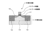
以下、本発明の半導体装置の一実施形態に係る第1例を、図1の概略構成断面図によって説明する。図1では、一例として、NMOSFETについて説明する。 Hereinafter, a first example according to an embodiment of a semiconductor device of the present invention will be described with reference to a schematic cross-sectional view of FIG. In FIG. 1, an NMOSFET will be described as an example.
図1に示すように、半導体基板11に素子分離領域12が形成され、素子形成領域13が区画されている。上記半導体基板11には、一例としてシリコン基板を用い、上記素子分離領域12は、例えばSTI(Shallow Trench Isolation)構造とする。なお、素子分離領域12の構造は、特に限定はされず、LOCOS(Local Oxidation of Silicon)構造、改良LOCOS構造等、種々の素子分離構造を採用することも可能である。上記半導体基板11の素子形成領域13上にはゲート絶縁膜14を介してゲート電極15が形成されている。上記ゲート絶縁膜14は、例えば酸化シリコン膜もしくは高誘電率膜(例えばハフニウムオキサイド(HfOx)、ハフニウムシリケート(HfSiOx)、ハフニウムアルミネート(HfAlOx)等)で形成されている。上記ゲート電極15は、ハフニウムと窒素とを含む膜で形成されている。したがって、ゲート電極15のゲート絶縁膜14側は少なくともハフニウムと窒素とを含む膜で形成されることになる。また、ゲート電極15の両側における半導体基板11にはソース・ドレイン領域16、17が形成されている。
As shown in FIG. 1, an
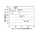
次に、ハフニウムと窒素とを含む膜(HfNx膜)中の窒素の組成比と移動度の関係について、図2および図3により説明する。図2では、縦軸に電子の移動度を示し、横軸に窒化ハフニウム中の窒素の組成比を示し、図3では、縦軸に電子の移動度を示し、横軸にゲートにかかる電界を示す。 Next, the relationship between the composition ratio and mobility of nitrogen in the film containing hafnium and nitrogen (HfN x film) will be described with reference to FIGS. In FIG. 2, the vertical axis represents the electron mobility, the horizontal axis represents the nitrogen composition ratio in hafnium nitride, and in FIG. 3, the vertical axis represents the electron mobility, and the horizontal axis represents the electric field applied to the gate. Show.
図2および図3に示すように、ハフニウム(Hf)のみでゲート電極を形成した場合には、ポリシリコンゲート電極に近い移動度を得ることができ、また、少なくとも窒素を含み、窒素の組成比が51%以下であれば、ポリシリコンゲート電極やハフニウムゲート電極を用いた場合とほぼ同等の280cm2/Vs(電界Eeff=0.8MV/cmにおける値)程度以上の移動度を得ることができる。特にゲート長が45nm以下の世代のトランジスタでは移動度がポリシリコンゲート電極を用いたトランジスタで得られる移動度の85%程度以上の移動度を確保したいという要求がある。このような要求も窒素の組成比を51%以下とすることで満たすことができる。 As shown in FIGS. 2 and 3, when the gate electrode is formed only of hafnium (Hf), mobility close to that of the polysilicon gate electrode can be obtained, and at least nitrogen is contained, and the composition ratio of nitrogen If it is 51% or less, a mobility of about 280 cm 2 / Vs (a value at an electric field Eeff = 0.8 MV / cm) or more, which is almost equivalent to the case where a polysilicon gate electrode or a hafnium gate electrode is used, can be obtained. . In particular, in the generation of transistors having a gate length of 45 nm or less, there is a demand for securing mobility of about 85% or more of the mobility obtained by a transistor using a polysilicon gate electrode. Such a requirement can also be satisfied by setting the nitrogen composition ratio to 51% or less.
また、ゲート長が45nm以下の世代のトランジスタでは、酸化シリコンのゲート絶縁膜の代わりに、酸化シリコンよりも誘電率の高い、いわゆる高誘電率膜(high−k膜)を用いるようになるといわれている。図4に示すように、ゲート電極にハフニウムと窒素とを含む膜(HfNx膜)を用いた場合、高誘電率膜を用いたトランジスタのほうがゲート絶縁膜に酸化シリコン膜を用いたトランジスタよりも移動度が高くなる。図示はしていないが、同様に、膜中の窒素の組成比が51%以下とするハフニウムと窒素とを含む膜(HfNx膜)を用いたゲート電極のトランジスタでも、酸化シリコン膜をゲート絶縁膜に用いた場合よりも高い移動度を得ることが可能になる。 In addition, it is said that in a generation of transistors having a gate length of 45 nm or less, a so-called high dielectric constant film (high-k film) having a dielectric constant higher than that of silicon oxide is used instead of a silicon oxide gate insulating film. Yes. As shown in FIG. 4, when a film containing hafnium and nitrogen (HfN x film) is used for the gate electrode, a transistor using a high dielectric constant film is more than a transistor using a silicon oxide film as a gate insulating film. Increases mobility. Although not shown, the silicon oxide film is similarly gate-insulated in a gate electrode transistor using a film containing hafnium and nitrogen (HfN x film) in which the composition ratio of nitrogen in the film is 51% or less. It is possible to obtain a higher mobility than when used for a film.
上記図2〜図4によって説明したように、ゲート電極15に用いるハフニウムと窒素とを含む膜(HfNx膜)の窒素の組成比〔N/(Hf+N)〕は、51%以下とすることが好ましく、より好ましくはポリシリコン電極を用いた場合とほぼ同等の移動度が得られるように、窒素の組成比を50%以下とする。
As described with reference to FIGS. 2 to 4 above, the nitrogen composition ratio [N / (Hf + N)] of the film containing hafnium and nitrogen (HfN x film) used for the
上記半導体装置1では、ゲート電極15がハフニウムと窒素とを含む膜からなり、その窒素の組成比が少なくとも窒素を含み51%以下であることから、本発明の半導体装置1は、従来から用いられているPoly−Si電極とほぼ同レベルの良好な移動度を得ることが可能になる。また、MOSFETに適した仕事関数を有する材料に少量の窒素(N2)を添加することによって形成することもできるため、MOSFETに適した仕事関数が得られ、MOSFETに適したしきい値電圧(Vth)を得ることができるので、MOSFETの性能の向上が図れる。また、少なくともゲート絶縁膜との界面にはハフニウムと窒素との化合物が形成されるため、下地のゲート絶縁膜との反応性を低減することができるので、ゲートリークが抑制できて、ゲート絶縁膜の薄膜化を実現することが可能になるという利点がある。
In the
次に、本発明の半導体装置の一実施形態に係る第2例を、図5の概略構成断面図によって説明する。 Next, a second example according to an embodiment of the semiconductor device of the present invention will be described with reference to a schematic sectional view of FIG.
図5に示すように、半導体基板11に素子分離領域12が形成され、素子形成領域13が区画されている。上記半導体基板11には、一例としてシリコン基板を用い、上記素子分離領域12は、例えばSTI(Shallow Trench Isolation)構造とする。なお、素子分離領域12の構造は、特に限定はされず、LOCOS(Local Oxidation of Silicon)構造、改良LOCOS構造等、種々の素子分離構造を採用することも可能である。上記半導体基板11の素子形成領域13上にはゲート絶縁膜14を介してゲート電極15が形成されている。上記ゲート絶縁膜14は、例えば酸化シリコン膜もしくは高誘電率膜(例えばハフニウムオキサイド(HfOx)、ハフニウムシリケート(HfSiOx)、ハフニウムアルミネート(HfAlOx)等)で形成されている。上記ゲート電極15は、上記ゲート絶縁膜14側のハフニウムと窒素とを含む膜18とその上層の導電膜19とで形成されている。したがって、ゲート電極15のゲート絶縁膜14側は少なくともハフニウムと窒素とを含む膜18で形成されることになる。また、ゲート電極15の両側における半導体基板11にはソース・ドレイン領域16、17が形成されている。
As shown in FIG. 5, an
上記導電膜19は、例えば、多結晶シリコン膜、1層以上の金属膜もしくは金属化合物膜、多結晶シリコン膜と金属膜との積層膜、または多結晶シリコン膜と金属化合物膜との積層膜とからなる。上記金属膜には、例えば、タングステン膜、タンタル膜等を用いることができ、上記金属化合物膜には、例えば、窒化タンタル膜、窒化チタン膜、窒化タングステン等を用いることができる。
The
上記ハフニウムと窒素とを含む膜(HfNx膜)18は、上記図2〜図4によって説明したように、ゲート電極15に用いるハフニウムと窒素とを含む膜(HfNx膜)の窒素の組成比〔N/(Hf+N)〕は、51%以下とすることが好ましく、より好ましくは、ポリシリコン電極を用いた場合とほぼ同等の移動度が得られるように、窒素の組成比を50%以下とする。
The film (HfN x film) 18 containing hafnium and nitrogen is the composition ratio of nitrogen of the film containing hafnium and nitrogen (HfN x film) used for the
上記半導体装置2では、ゲート電極15の少なくともゲート絶縁膜14側がハフニウムと窒素とを含む膜からなり、その窒素の組成比が少なくとも窒素を含み51%以下であることから、本発明の半導体装置2は、従来から用いられているPoly−Si電極とほぼ同レベルの良好な移動度を得ることが可能になる。また、MOSFETに適した仕事関数を有する材料に少量の窒素(N2)を添加することによって形成することもできるため、MOSFETに適した仕事関数が得られ、MOSFETに適したしきい値電圧(Vth)を得ることができるので、MOSFETの性能の向上が図れる。また、少なくともゲート絶縁膜との界面にはハフニウムと窒素との化合物が形成されるため、下地のゲート絶縁膜との反応性を低減することができるので、ゲートリークが抑制できて、ゲート絶縁膜の薄膜化を実現することが可能になるという利点がある。
In the
上記半導体装置1、2では、ゲート電極の構造としてプレーナ構造で説明したが、埋め込み型ゲート構造(例えばダマシンゲート構造)でも、上記ゲート電極を適用することができる。
In the
次に、本発明の半導体装置の一実施形態に係る第3例として埋め込み型ゲート構造の半導体装置の一例を、図6の概略構成断面図によって説明する。 Next, an example of a semiconductor device having a buried gate structure as a third example according to an embodiment of the semiconductor device of the present invention will be described with reference to the schematic cross-sectional view of FIG.
図6に示すように、半導体基板11には、トランジスタの形成領域を分離する素子分離領域12が、例えばSTI(Shallow Trench Isolation )技術により形成されている。この素子分離領域12はLOCOS(Local Oxidation of Silicon )技術により形成されたものであってもよい。上記半導体基板11のトランジスタの形成領域にはウエル(図示せず)が形成されていてもよい。また、上記ウエルの上層にしきい値電圧を調整するための不純物が導入されていてもよい。
As shown in FIG. 6, an
上記半導体基板11上には、第1絶縁膜31と第2絶縁膜32とが積層して形成され、この第1絶縁膜31と第2絶縁膜32のトランジスタの形成領域には溝33が形成されている。上記溝33の内面には、ゲート絶縁膜34が形成されている。さらに、上記溝33の内部には上記ゲート絶縁膜34を介してゲート電極35が形成されている。このゲート電極35は、例えば、ゲート絶縁膜34側がハフニウムと窒素とを含む膜38で形成され、その上層が導電膜39で形成されている。このハフニウムと窒素とを含む膜38は、窒素の組成比が少なくとも窒素を含み51%以下となるように形成されている。また、上記ゲート絶縁膜34は、例えば酸化シリコン膜もしくは高誘電率膜(例えばハフニウムオキサイド(HfOx)、ハフニウムシリケート(HfSiOx)、ハフニウムアルミネート(HfAlOx)等)で形成されている。
A first insulating
上記ゲート電極15は、ハフニウムと窒素とを含む膜38と導電膜39との積層構造としたが、ハフニウムと窒素とを含む膜38の単層構造として溝33内をハフニウムと窒素とを含む膜38で埋め込む構造とすることもできる。
The
また、トランジスタがLDD(Lightly Doped Drain)構造をなしている場合には、上記ゲート電極35の両側における上記半導体基板11上層には低濃度層41、42が形成されている。また上記ゲート電極35の側壁にはサイドウォール43が形成されている。さらに上記ゲート電極35の両側における上記半導体基板11(ウエル領域)上層には、上記低濃度層41、42を介してトランジスタのソース・ドレイン領域45、46が形成されている。
When the transistor has an LDD (Lightly Doped Drain) structure, low-
上記半導体装置3では、ゲート電極35の少なくともゲート絶縁膜34側がハフニウムと窒素とを含む膜38からなり、その窒素の組成比が少なくとも窒素を含み51%以下であることから、本発明の半導体装置3は、従来から用いられているPoly−Si電極とほぼ同レベルの良好な移動度を得ることが可能になる。また、MOSFETに適した仕事関数を有する材料に少量の窒素(N2)を添加することによって形成することもできるため、MOSFETに適した仕事関数が得られるので、MOSFETに適したしきい値電圧(Vth)を得ることができ、MOSFETの性能の向上が図れる。少なくともゲート絶縁膜34との界面にはハフニウムと窒素との化合物が形成されるため、下地のゲート絶縁膜34との反応性を低減することができるので、ゲートリークが抑制できて、ゲート絶縁膜34の薄膜化を実現することが可能になるという利点がある。
In the
また、ゲート電極35をハフニウムと窒素とを含む膜38と導電膜39との積層構造とすることによりハフニウムと窒素とを含む膜38の膜厚を薄膜化することができる。これによって、下地のゲート絶縁膜34と反応するハフニウムの量を低減することが可能になるので、ゲート電極35にハフニウムと窒素とを含む膜38を用いたことによるゲート絶縁膜14の薄膜化をさらに抑制することができる。
Further, the
次に、本発明の半導体装置の製造方法の一実施形態に係る第1例を、図7の製造工程断面図によって説明する。この製造方法は、前記図1によって説明した半導体装置1の製造方法である。
Next, a first example according to an embodiment of the method for manufacturing a semiconductor device of the present invention will be described with reference to the manufacturing process sectional view of FIG. This manufacturing method is a manufacturing method of the
図7(1)に示すように、半導体基板11に素子分離領域12を形成し、素子形成領域13を区画する。上記半導体基板11には、一例としてシリコン基板を用い、上記素子分離領域12を、例えばSTI(Shallow Trench Isolation)構造に形成する。なお、素子分離領域12の構造は、特に限定はされず、LOCOS(Local Oxidation of Silicon)構造、改良LOCOS構造等を採用することも可能である。上記半導体基板11上にゲート絶縁膜14を形成する。このゲート絶縁膜14は例えば酸化シリコン膜、もしくはハフニウムオキサイド(HfOx)、ハフニウムシリケート(HfSiOx)、ハフニウムアルミネート(HfAlOx)等の高誘電率膜で形成する。
As shown in FIG. 7A, an
次いで、図7(2)に示すように、ゲート絶縁膜14上にゲート電極形成膜51を形成する。上記ゲート電極形成膜51は、例えばハフニウムと窒素とを含む膜(HfNx膜)で形成され、その成膜方法の一例としてはスパッタリング法を用いることができる。上記HfNx膜は、ハフニウムと窒素とに対する窒素の組成比〔N/(Hf+Si)〕が少なくとも窒素を含み51%以下になる条件で成膜する。上記窒素の組成比を少なくとも窒素を含み51%以下とするのは、前記図2〜図4によって説明した通りである。
Next, as illustrated in FIG. 7B, a gate
上記ハフニウムと窒素とを含む膜(HfNx膜)の成膜条件の一例を以下に説明する。成膜条件としては、スパッタリングのターゲットにハフニウムを用いる。プロセス雰囲気の圧力を13.3mPa以上13.3Pa以下の範囲で設定し、プロセスガスにArと窒素との混合ガスを用いる。その際、アルゴン(Ar)に対する窒素の流量比を0.2以下とすることが好ましい。また基板温度を室温以上150℃以下の範囲に設定する。なお、HfNx膜のスパッタ成膜条件は上記に限定する必要は無く、例えばターゲットとしてN組成比が51%以下であるようなHfNxを用いても良い。また成膜方法をスパッタリング法に限定する必要も無く、例えば化学的気相成長(CVD)法によって成膜を行うこともできる。 An example of film formation conditions for the film containing hafnium and nitrogen (HfN x film) will be described below. As film formation conditions, hafnium is used as a sputtering target. The pressure of the process atmosphere is set in the range of 13.3 mPa to 13.3 Pa, and a mixed gas of Ar and nitrogen is used as the process gas. At that time, the flow rate ratio of nitrogen to argon (Ar) is preferably 0.2 or less. The substrate temperature is set in the range of room temperature to 150 ° C. The sputter deposition conditions for the HfN x film need not be limited to the above. For example, HfN x having an N composition ratio of 51% or less may be used as a target. Further, it is not necessary to limit the film forming method to the sputtering method, and the film can be formed by, for example, a chemical vapor deposition (CVD) method.
その後、図7(3)に示すように、例えば通常のレジスタ塗布、フォトリソグラフィー技術およびエッチング技術によって、上記ゲート電極形成膜51をエッチング加工して、ゲート絶縁膜14上にゲート電極形成膜51からなるゲート電極15を形成する。さらに、通常のMOSトランジスタのソース・ドレイン領域の形成技術によって、ゲート電極15の両側における半導体基板11にソース・ドレイン領域16、17を形成する。このソース・ドレイン領域16、17は、図示はしないが、例えばLDD(Lightly Doped Drain)構造としてもよい。このようにして、半導体装置1を得ることができる。
Thereafter, as shown in FIG. 7 (3), the gate
上記半導体装置1の製造方法では、ゲート電極15がハフニウムと窒素とを含む膜で形成され、その窒素の組成比が少なくとも窒素を含み51%以下となるように成膜されることから、本発明の半導体装置は、従来から用いられているPoly−Si電極と同レベルの良好な移動度を得ることが可能になる。また、MOSFETに適した仕事関数を有する材料に少量の窒素(N2)を添加することによって形成できるため、MOSFETに適した仕事関数が得られるので、MOSFETに適したしきい値電圧(Vth)を得ることができる。よって、性能の高いMOSFETを製造することができる。また、少なくともゲート絶縁膜との界面にはハフニウムと窒素との化合物が形成されるため、下地のゲート絶縁膜との反応性を低減することができるので、ゲートリークが抑制できて、ゲート絶縁膜の薄膜化を実現することが可能になるという利点がある。
In the method for manufacturing the
次に、本発明の半導体装置の製造方法の一実施形態に係る第2例を、図8の製造工程断面図によって説明する。この製造方法は前記図5によって説明した半導体装置2の製造方法である。
Next, a second example according to an embodiment of the method for manufacturing a semiconductor device of the present invention will be described with reference to the manufacturing process sectional view of FIG. This manufacturing method is the manufacturing method of the
図8(1)に示すように、半導体基板11に素子分離領域12を形成し、素子形成領域13を区画する。上記半導体基板11には、一例としてシリコン基板を用い、上記素子分離領域12を、例えばSTI(Shallow Trench Isolation)構造に形成する。なお、素子分離領域12の構造は、特に限定はされず、LOCOS(Local Oxidation of Silicon)構造、改良LOCOS構造等を採用することも可能である。上記半導体基板11上にゲート絶縁膜14を形成する。このゲート絶縁膜14は例えば酸化シリコン膜、もしくはハフニウムオキサイド(HfOx)、ハフニウムシリケート(HfSiOx)、ハフニウムアルミネート(HfAlOx)等の高誘電率膜で形成する。
As shown in FIG. 8A, an
次に、図8(2)に示すように、ゲート絶縁膜14上にゲート電極形成膜51の下層部分を、例えばハフニウムと窒素とを含む膜(HfNx膜)18で形成する。その成膜方法の一例としてはスパッタリング法を用いることができる。上記HfNx膜は、ハフニウムと窒素とに対する窒素の組成比〔N/(Hf+Si)〕が少なくとも窒素を含み51%以下になる条件で成膜する。上記窒素の組成比を少なくとも窒素を含み51%以下とするのは、前記図2〜図4によって説明したとおりである。
Next, as shown in FIG. 8B, the lower layer portion of the gate
上記ハフニウムと窒素とを含む膜(HfNx膜)18の成膜条件の一例を以下に説明する。成膜条件としては、スパッタリングのターゲットにハフニウムを用いる。プロセス雰囲気の圧力を13.3mPa以上13.3Pa以下の範囲で設定し、プロセスガスにArと窒素との混合ガスを用いる。その際、アルゴン(Ar)に対する窒素の流量比を0.2以下とすることが好ましい。また基板温度を室温以上150℃以下の範囲に設定する。なお、HfNx膜のスパッタ成膜条件は上記に限定する必要は無く、例えばターゲットとしてN組成比が51%以下であるようなHfNxを用いても良い。また成膜方法をスパッタリング法に限定する必要も無く、例えば化学的気相成長(CVD)法によって成膜を行うこともできる。 An example of film formation conditions for the film (HfN x film) 18 containing hafnium and nitrogen will be described below. As film formation conditions, hafnium is used as a sputtering target. The pressure of the process atmosphere is set in the range of 13.3 mPa to 13.3 Pa, and a mixed gas of Ar and nitrogen is used as the process gas. At that time, the flow rate ratio of nitrogen to argon (Ar) is preferably 0.2 or less. The substrate temperature is set in the range of room temperature to 150 ° C. The sputter deposition conditions for the HfN x film need not be limited to the above. For example, HfN x having an N composition ratio of 51% or less may be used as a target. Further, it is not necessary to limit the film forming method to the sputtering method, and the film can be formed by, for example, a chemical vapor deposition (CVD) method.
次に、図8(3)に示すように、上記ハフニウムと窒素とを含む膜(HfNx膜)18上に上部電極膜19を成膜して、ゲート電極形成膜51を形成する。上記上部電極膜19は、例えば、多結晶シリコン膜、1層以上の金属膜もしくは金属化合物膜、多結晶シリコン膜と金属膜との積層膜、または多結晶シリコン膜と金属化合物膜との積層膜で形成することができる。上記金属膜には、例えば、タングステン膜、タンタル等を用いることができ、上記金属化合物膜には、例えば、窒化タンタル膜、窒化チタン膜、窒化タングステン等を用いることができる。
Next, as shown in FIG. 8C, an
上記上部電極膜19の成膜条件の一例を以下に説明する。成膜方法として、例えばCVD法を用いる。成膜条件の一例として、プロセスガスに四塩化チタン(TiCl4)とアンモニア(NH3)とを用い、プロセス雰囲気の圧力を13.3Pa以上1.33kPa以下の範囲で設定し、また基板温度を400℃以上600℃以下の範囲に設定する。なお、上部電極膜19の成膜方法は上記に限定する必要は無く、スパッタリング法を用いて成膜することもできる。
An example of the conditions for forming the
その後、図8(4)に示すように、例えば通常のレジスタ塗布、フォトリソグラフィー技術およびエッチング技術によって、上記ゲート電極形成膜21をエッチング加工して、ゲート絶縁膜14上にゲート電極形成膜51からなるゲート電極15を形成する。さらに、通常のMOSトランジスタのソース・ドレイン領域の形成技術によって、ゲート電極15の両側における半導体基板11にソース・ドレイン領域16、17を形成する。このソース・ドレイン領域16、17は、図示はしないが、例えばLDD(Lightly Doped Drain)構造としてもよい。このようにして、半導体装置2を得ることができる。
Thereafter, as shown in FIG. 8 (4), the gate electrode forming film 21 is etched by, for example, ordinary register coating, photolithography technique, and etching technique, so that the gate
上記半導体装置2の製造方法では、ゲート電極15の少なくともゲート絶縁膜14側がハフニウムと窒素とを含む膜で形成され、その窒素の組成比が少なくとも窒素を含み51%以下となるように成膜されることから、本発明の半導体装置は、従来から用いられているPoly−Si電極と同レベルの良好な移動度を得ることが可能になる。また、MOSFETに適した仕事関数を有する材料に少量の窒素(N2)を添加することによって形成できるため、MOSFETに適した仕事関数が得られるので、MOSFETに適したしきい値電圧(Vth)を得ることができる。よって、性能の高いMOSFETを製造することができる。また、少なくともゲート絶縁膜との界面にはハフニウムと窒素との化合物が形成されるため、下地のゲート絶縁膜との反応性を低減することができるので、ゲートリークが抑制できて、ゲート絶縁膜の薄膜化を実現することが可能になるという利点がある。
In the manufacturing method of the
さらに、上記半導体装置2の製造方法では、ゲート電極15をハフニウムと窒素とを含む膜18と上部電極膜19との積層構造で形成することから、ハフニウムと窒素とを含む膜(HfNx膜)18を薄く形成することができる。このため、ハフニウムと窒素とを含む膜18の膜厚を薄膜化することができる。これによって、下地のゲート絶縁膜14と反応するハフニウムの量を低減することが可能になるので、ゲート電極15にハフニウムと窒素とを含む膜18を用いたことによるゲート絶縁膜14の薄膜化をさらに抑制することができる。
Further, in the manufacturing method of the
次に、本発明の半導体装置の製造方法の一実施形態に係る第3例を、図9、10の製造工程断面図によって説明する。この製造方法は前記図6によって説明した半導体装置3の製造方法である。
Next, a third example according to an embodiment of the semiconductor device manufacturing method of the present invention will be described with reference to the manufacturing process cross-sectional views of FIGS. This manufacturing method is the manufacturing method of the
図9(1)に示すように、半導体基板11としてシリコン基板を用意する。この半導体基板11に例えば通常のトレンチ素子分離形成技術によって、トランジスタの形成領域13を分離する素子分離領域12を形成する。その後、トランジスタの形成領域にウエル(図示せず)を形成する。
As shown in FIG. 9A, a silicon substrate is prepared as the
次に、しきい値電圧調整用の不純物をウエルに導入した後、上記半導体基板11のトランジスタの形成領域上に第1絶縁膜(ダミーゲート絶縁膜)71を形成する。この第1絶縁膜31は、例えばシリコン酸化膜を10nmの厚さに堆積して形成される。
Next, after an impurity for adjusting the threshold voltage is introduced into the well, a first insulating film (dummy gate insulating film) 71 is formed on the transistor formation region of the
次に、上記半導体基板11上に第1絶縁膜31を介してダミーゲート電極71を形成する。このダミーゲート電極71は、一例として、CVDによって多結晶シリコン膜を100nmの厚さに成膜する。次いで、通常のレジスト塗布、リソグラフィー技術によるレジストによるエッチングマスクを形成した後、そのエッチングマスクを用いて多結晶シリコン膜を異方性エッチングによりパターンニングすることで形成される。
Next, a
次に、上記ダミーゲート電極71の両側における上記半導体基板11にソース・ドレインを形成する。具体的には、イオン注入法によって、ダミーゲート電極71の両側における半導体基板11にLDD(Lightly Doped Drain)領域41、42を形成する。次いで、上記ダミーゲート電極71を被覆するサイドウォール形成膜を成膜した後、このサイドウォール形成膜をエッチバックして、ダミーゲート電極71の両側にサイドウォール絶縁膜43を形成する。次いで、イオン注入法によって、ダミーゲート電極71の一方側の半導体基板11に上記LDD領域41を介してソース・ドレイン領域45を形成するとともにダミーゲート電極71の他方側の半導体基板11に上記LDD領域42を介してソース・ドレイン領域46を形成する。
Next, a source / drain is formed in the
次に、図9(2)に示すように、上記半導体基板11に形成された第1絶縁膜31上にダミーのゲート電極71を被覆する第2絶縁膜32を形成する。この第2絶縁膜32は、配線との層間絶縁膜になるものであり、例えば化学的気相成長(以下CVDという、CVDはChemical Vapor Depositionの略)法によって、酸化シリコンを堆積して形成する。この厚さは、例えば、ダミーゲート電極71よりも全面にわたって高くなるような厚さに形成することが好ましい。次に、化学的機械研磨(以下CMPという、CMPはChemical Mechanical Polishing)法によって、上記第2絶縁膜32を研磨して上記各ダミーゲート電極71上部を露出させるとともに平坦化する。
Next, as shown in FIG. 9B, a second insulating
その後、エッチングによって、上記ダミーゲート電極71を除去する。この結果、図9(3)に示すように、上記サイドウォール絶縁膜43を側壁とする溝33が形成される。
Thereafter, the
次に、図10(4)に示すように、上記各溝33の内面にゲート絶縁膜34を形成する。このゲート絶縁膜34は、例えば、ハフニウムオキサイド(HfOx)、ハフニウムシリケート(HfSiOx)、ハフニウムアルミネート(HfAlOx)等の高誘電率膜で形成する。もしくは酸化シリコン膜で形成する。
Next, as shown in FIG. 10 (4), a
次に、例えばスパッタリング法によって、上記ゲート絶縁膜34上の上記溝33内部にハフニウムと窒素とを含む膜(HfNx膜)38を形成する。
Next, a film (HfN x film) 38 containing hafnium and nitrogen is formed inside the
上記ハフニウムと窒素とを含む膜(HfNx膜)38の成膜条件の一例を以下に説明する。成膜条件としては、スパッタリングのターゲットにハフニウムを用いる。プロセス雰囲気の圧力を13.3mPa以上13.3Pa以下の範囲で設定し、プロセスガスにArと窒素との混合ガスを用いる。その際、アルゴン(Ar)に対する窒素の流量比を0.2以下とすることが好ましい。また基板温度を室温以上150℃以下の範囲に設定する。なお、HfNx膜のスパッタ成膜条件は上記に限定する必要は無く、例えばターゲットとしてN組成比が51%以下であるようなHfNxを用いても良い。また成膜方法をスパッタリング法に限定する必要も無く、例えば化学的気相成長(CVD)法によって成膜を行うこともできる。 An example of film formation conditions for the film (HfN x film) 38 containing hafnium and nitrogen will be described below. As film formation conditions, hafnium is used as a sputtering target. The pressure of the process atmosphere is set in the range of 13.3 mPa to 13.3 Pa, and a mixed gas of Ar and nitrogen is used as the process gas. At that time, the flow rate ratio of nitrogen to argon (Ar) is preferably 0.2 or less. The substrate temperature is set in the range of room temperature to 150 ° C. The sputter deposition conditions for the HfN x film need not be limited to the above. For example, HfN x having an N composition ratio of 51% or less may be used as a target. Further, it is not necessary to limit the film forming method to the sputtering method, and the film can be formed by, for example, a chemical vapor deposition (CVD) method.
さらに、上記溝33内部を完全に埋め込むように、上記ハフニウムと窒素とを含む膜(HfNx膜)38上に導電膜39を成膜して、ゲート電極形成膜51を形成する。上記導電膜39は、例えば、多結晶シリコン膜、1層以上の金属膜もしくは金属化合物膜、多結晶シリコン膜と金属膜との積層膜、または多結晶シリコン膜と金属化合物膜との積層膜で形成することができる。上記金属膜には、例えば、タングステン膜、タンタル等を用いることができ、上記金属化合物膜には、例えば、窒化タンタル膜、窒化チタン膜、窒化タングステン等を用いることができる。
Further, a
上記導電膜39の成膜条件の一例を以下に説明する。成膜方法として、例えばCVD法を用いる。成膜条件の一例として、プロセスガスに四塩化チタン(TiCl4)とアンモニア(NH3)とを用い、プロセス雰囲気の圧力を13.3Pa以上1.33kPa以下の範囲で設定し、また基板温度を400℃以上600℃以下の範囲に設定する。なお、導電膜39の成膜方法は上記に限定する必要は無く、スパッタリング法を用いて成膜することもできる。
An example of film formation conditions for the
次に、図10(5)に示すように、CMP法によって、溝33以外の部分の上記ハフニウムと窒素とを含む膜(HfNx膜)38と導電膜39とを除去して平坦化して、溝33の内部のみに残した上記ハフニウムと窒素とを含む膜(HfNx膜)38と導電膜39とからなるゲート電極35を形成する。
Next, as shown in FIG. 10 (5), by CMP, the film (HfN x film) 38 and the
このようにして、埋め込みゲート構造の半導体装置3が形成される。
In this way, the
上記半導体装置3の製造方法では、ゲート電極35の少なくともゲート絶縁膜34側がハフニウムと窒素とを含む膜38で形成され、その窒素の組成比が少なくとも窒素を含み51%以下となるように成膜されることから、本発明の半導体装置3は、従来から用いられているPoly−Si電極と同レベルの良好な移動度を得ることが可能になる。また、MOSFETに適した仕事関数を有する材料に少量の窒素(N2)を添加することによって形成できるため、MOSFETに適した仕事関数が得られるので、MOSFETに適したしきい値電圧(Vth)を得ることができる。よって、性能の高いMOSFETを製造することができる。また、少なくともゲート絶縁膜34との界面にはハフニウムと窒素との化合物が形成されるため、下地のゲート絶縁膜34との反応性を低減することができるので、ゲートリークが抑制できて、ゲート絶縁膜34の薄膜化を実現することが可能になるという利点がある。
In the method of manufacturing the
さらに、上記半導体装置3の製造方法では、ゲート電極35をハフニウムと窒素とを含む膜38と導電膜39との積層構造で形成することから、ハフニウムと窒素とを含む膜(HfNx膜)38を薄く形成することができる。このため、ハフニウムと窒素とを含む膜38の膜厚を薄膜化することができる。これによって、下地のゲート絶縁膜34と反応するハフニウムの量を低減することが可能になるので、ゲート電極35にハフニウムと窒素とを含む膜38を用いたことによるゲート絶縁膜34の薄膜化をさらに抑制することができる。
Further, in the manufacturing method of the
上記半導体装置および半導体装置の製造方法において、上記ハフニウムと窒素とを含む膜は、窒素の組成比が51%以下であれば、ハフニウムと窒素以外の元素も含ませることができる。そのような元素としては、例えば、炭素(C)、タンタル(Ta)、チタン(Ti)、タングステン(W)、ジルコニウム(Zr)、モリブデン(Mo)等が挙げられる。上記元素のうち、タンタル(Ta)、ジルコニウム(Zr)はハフニウムと同程度(4.0eV程度)の仕事関数値を有している。また、チタン(Ti)、タングステン(W)、モリブデン(Mo)はハフニウムより大きな仕事関数値を有していて、その値はミッドギャップ付近(4.6eV程度)である。これらの金属をハフニウムと窒素とを含む膜に添加すると、添加した金属の仕事関数値の方向に仕事関数が移行するので、ゲート電極の仕事関数値の調整にこれらの金属を添加することもできる。 In the semiconductor device and the method for manufacturing a semiconductor device, the film containing hafnium and nitrogen can contain elements other than hafnium and nitrogen as long as the composition ratio of nitrogen is 51% or less. Examples of such elements include carbon (C), tantalum (Ta), titanium (Ti), tungsten (W), zirconium (Zr), molybdenum (Mo), and the like. Of the above elements, tantalum (Ta) and zirconium (Zr) have work function values similar to hafnium (about 4.0 eV). Titanium (Ti), tungsten (W), and molybdenum (Mo) have a work function value larger than that of hafnium, and the value is near the mid gap (about 4.6 eV). When these metals are added to a film containing hafnium and nitrogen, the work function shifts in the direction of the work function value of the added metal. Therefore, these metals can be added to adjust the work function value of the gate electrode. .
また、本発明の半導体装置および半導体装置の製造方法によれば、NMOSFETに適したしきい値電圧(Vth)が得られる。そして、ハフニウムと窒素とを含む膜を用いたゲート電極と下地のゲート絶縁膜との反応性を低減することが可能になるので、ゲートリークを抑制することができ、ゲート絶縁膜の薄膜化を実現することが可能になる。また、ハフニウムと窒素とを含む膜の膜厚をより薄膜化することによって、ハフニウムと窒素とを含む膜のハフニウムと下地のゲート絶縁膜との反応量を低減することが可能になり、ゲート絶縁膜の薄膜化をさらに抑制することができる。 Further, according to the semiconductor device and the method of manufacturing the semiconductor device of the present invention, a threshold voltage (Vth) suitable for NMOSFET can be obtained. And, it becomes possible to reduce the reactivity between the gate electrode using the film containing hafnium and nitrogen and the underlying gate insulating film, so that gate leakage can be suppressed and the gate insulating film can be made thinner. Can be realized. Further, by reducing the film thickness of the film containing hafnium and nitrogen, it becomes possible to reduce the amount of reaction between the hafnium of the film containing hafnium and nitrogen and the underlying gate insulating film. Thinning of the film can be further suppressed.
1…半導体装置、11…半導体基板、14…ゲート絶縁膜、15…ゲート電極
DESCRIPTION OF
Claims (2)
前記ゲート電極は少なくとも前記ゲート絶縁膜側がハフニウムと窒素とを含む膜からなり、
前記ハフニウムと窒素とを含む膜は少なくとも窒素を含みかつハフニウムと窒素とに対する窒素の組成比が51%以下である
ことを特徴とする半導体装置。 A semiconductor device comprising a field effect transistor having a gate electrode on a semiconductor substrate via a gate insulating film,
The gate electrode is made of a film containing at least the gate insulating film side containing hafnium and nitrogen,
The semiconductor device characterized in that the film containing hafnium and nitrogen contains at least nitrogen and a composition ratio of nitrogen to hafnium and nitrogen is 51% or less.
前記ゲート電極を形成する工程は少なくとも前記ゲート絶縁膜側をハフニウムと窒素とを含む膜で形成する工程を含み、
前記ハフニウムと窒素とを含む膜は少なくとも窒素を含みかつハフニウムと窒素とに対する窒素の組成比が51%以下の膜で形成される
ことを特徴とする半導体装置の製造方法。
A method for manufacturing a semiconductor device comprising a step of forming a gate electrode on a semiconductor substrate via a gate insulating film,
The step of forming the gate electrode includes a step of forming at least the gate insulating film side with a film containing hafnium and nitrogen,
The method for manufacturing a semiconductor device, wherein the film containing hafnium and nitrogen includes at least nitrogen and a composition ratio of nitrogen to hafnium and nitrogen is 51% or less.
Priority Applications (1)
| Application Number | Priority Date | Filing Date | Title |
|---|---|---|---|
| JP2005114270A JP2006294894A (en) | 2005-04-12 | 2005-04-12 | Semiconductor apparatus and its manufacturing method |
Applications Claiming Priority (1)
| Application Number | Priority Date | Filing Date | Title |
|---|---|---|---|
| JP2005114270A JP2006294894A (en) | 2005-04-12 | 2005-04-12 | Semiconductor apparatus and its manufacturing method |
Publications (1)
| Publication Number | Publication Date |
|---|---|
| JP2006294894A true JP2006294894A (en) | 2006-10-26 |
Family
ID=37415135
Family Applications (1)
| Application Number | Title | Priority Date | Filing Date |
|---|---|---|---|
| JP2005114270A Pending JP2006294894A (en) | 2005-04-12 | 2005-04-12 | Semiconductor apparatus and its manufacturing method |
Country Status (1)
| Country | Link |
|---|---|
| JP (1) | JP2006294894A (en) |
Citations (5)
| Publication number | Priority date | Publication date | Assignee | Title |
|---|---|---|---|---|
| JP2000031296A (en) * | 1998-06-30 | 2000-01-28 | Motorola Inc | Cmos semiconductor element and manufacture thereof |
| JP2003273350A (en) * | 2002-03-15 | 2003-09-26 | Nec Corp | Semiconductor device and method for manufacturing the same |
| JP2005005603A (en) * | 2003-06-13 | 2005-01-06 | Toshiba Corp | Semiconductor device and its manufacturing method |
| JP2005142539A (en) * | 2003-10-17 | 2005-06-02 | Toshiba Corp | Semiconductor device and manufacturing method therefor |
| JP2006295123A (en) * | 2005-03-18 | 2006-10-26 | Fujitsu Ltd | Mos field effect semiconductor device and manufacturing method thereof |
-
2005
- 2005-04-12 JP JP2005114270A patent/JP2006294894A/en active Pending
Patent Citations (5)
| Publication number | Priority date | Publication date | Assignee | Title |
|---|---|---|---|---|
| JP2000031296A (en) * | 1998-06-30 | 2000-01-28 | Motorola Inc | Cmos semiconductor element and manufacture thereof |
| JP2003273350A (en) * | 2002-03-15 | 2003-09-26 | Nec Corp | Semiconductor device and method for manufacturing the same |
| JP2005005603A (en) * | 2003-06-13 | 2005-01-06 | Toshiba Corp | Semiconductor device and its manufacturing method |
| JP2005142539A (en) * | 2003-10-17 | 2005-06-02 | Toshiba Corp | Semiconductor device and manufacturing method therefor |
| JP2006295123A (en) * | 2005-03-18 | 2006-10-26 | Fujitsu Ltd | Mos field effect semiconductor device and manufacturing method thereof |
Similar Documents
| Publication | Publication Date | Title |
|---|---|---|
| US10505008B2 (en) | Method for manufacturing insulated gate field effect transistor | |
| US7229873B2 (en) | Process for manufacturing dual work function metal gates in a microelectronics device | |
| US7126199B2 (en) | Multilayer metal gate electrode | |
| US8294202B2 (en) | Metal gate structure of a semiconductor device | |
| US7279413B2 (en) | High-temperature stable gate structure with metallic electrode | |
| JP5326274B2 (en) | Semiconductor device and manufacturing method of semiconductor device | |
| JP4770885B2 (en) | Semiconductor device | |
| TWI458049B (en) | Semiconductor device and a method of manufacturing the same | |
| US20070178634A1 (en) | Cmos semiconductor devices having dual work function metal gate stacks | |
| JP2008147393A (en) | Semiconductor device and its manufacturing method therefor | |
| EP1848033A2 (en) | Semiconductor Device and Fabrication Method Therefor | |
| JP2009033032A (en) | Semiconductor device, and method of manufacturing semiconductor device | |
| JP2012004455A (en) | Method of manufacturing semiconductor device, and semiconductor device | |
| US9076857B2 (en) | Semiconductor device and manufacturing method thereof | |
| JP2008053283A (en) | Manufacturing method for semiconductor device | |
| JP2004319952A (en) | Semiconductor device and manufacturing method therefor | |
| TW201104837A (en) | Semiconductor device and the manufacturing method thereof | |
| JP2009059761A (en) | Semiconductor device and manufacturing method of semiconductor device | |
| US20080197429A1 (en) | Semiconductor device and method of manufacturing same | |
| US7391089B2 (en) | Semiconductor device and method of manufacturing the same | |
| JP2008244331A (en) | Semiconductor device and method of manufacturing the same | |
| JP2006294894A (en) | Semiconductor apparatus and its manufacturing method | |
| JP5195421B2 (en) | Semiconductor device | |
| JP2006086272A (en) | Semiconductor device | |
| JP2008130798A (en) | Semiconductor device, and manufacturing method thereof |
Legal Events
| Date | Code | Title | Description |
|---|---|---|---|
| A621 | Written request for application examination |
Free format text: JAPANESE INTERMEDIATE CODE: A621 Effective date: 20080306 |
|
| RD02 | Notification of acceptance of power of attorney |
Free format text: JAPANESE INTERMEDIATE CODE: A7422 Effective date: 20091009 |
|
| RD04 | Notification of resignation of power of attorney |
Free format text: JAPANESE INTERMEDIATE CODE: A7424 Effective date: 20091104 |
|
| A131 | Notification of reasons for refusal |
Free format text: JAPANESE INTERMEDIATE CODE: A131 Effective date: 20100511 |
|
| A977 | Report on retrieval |
Free format text: JAPANESE INTERMEDIATE CODE: A971007 Effective date: 20100513 |
|
| A521 | Written amendment |
Free format text: JAPANESE INTERMEDIATE CODE: A523 Effective date: 20100702 |
|
| A02 | Decision of refusal |
Free format text: JAPANESE INTERMEDIATE CODE: A02 Effective date: 20100727 |