JP2006269632A - Electric circuit board housing box - Google Patents
Electric circuit board housing box Download PDFInfo
- Publication number
- JP2006269632A JP2006269632A JP2005083952A JP2005083952A JP2006269632A JP 2006269632 A JP2006269632 A JP 2006269632A JP 2005083952 A JP2005083952 A JP 2005083952A JP 2005083952 A JP2005083952 A JP 2005083952A JP 2006269632 A JP2006269632 A JP 2006269632A
- Authority
- JP
- Japan
- Prior art keywords
- electric circuit
- connector
- board
- circuit board
- housing
- Prior art date
- Legal status (The legal status is an assumption and is not a legal conclusion. Google has not performed a legal analysis and makes no representation as to the accuracy of the status listed.)
- Granted
Links
Images


Classifications
-
- H—ELECTRICITY
- H05—ELECTRIC TECHNIQUES NOT OTHERWISE PROVIDED FOR
- H05K—PRINTED CIRCUITS; CASINGS OR CONSTRUCTIONAL DETAILS OF ELECTRIC APPARATUS; MANUFACTURE OF ASSEMBLAGES OF ELECTRICAL COMPONENTS
- H05K5/00—Casings, cabinets or drawers for electric apparatus
- H05K5/0026—Casings, cabinets or drawers for electric apparatus provided with connectors and printed circuit boards [PCB], e.g. automotive electronic control units
- H05K5/0065—Casings, cabinets or drawers for electric apparatus provided with connectors and printed circuit boards [PCB], e.g. automotive electronic control units wherein modules are associated together, e.g. electromechanical assemblies, modular structures
-
- B—PERFORMING OPERATIONS; TRANSPORTING
- B60—VEHICLES IN GENERAL
- B60R—VEHICLES, VEHICLE FITTINGS, OR VEHICLE PARTS, NOT OTHERWISE PROVIDED FOR
- B60R16/00—Electric or fluid circuits specially adapted for vehicles and not otherwise provided for; Arrangement of elements of electric or fluid circuits specially adapted for vehicles and not otherwise provided for
- B60R16/02—Electric or fluid circuits specially adapted for vehicles and not otherwise provided for; Arrangement of elements of electric or fluid circuits specially adapted for vehicles and not otherwise provided for electric constitutive elements
- B60R16/023—Electric or fluid circuits specially adapted for vehicles and not otherwise provided for; Arrangement of elements of electric or fluid circuits specially adapted for vehicles and not otherwise provided for electric constitutive elements for transmission of signals between vehicle parts or subsystems
- B60R16/0238—Electrical distribution centers
-
- G—PHYSICS
- G11—INFORMATION STORAGE
- G11B—INFORMATION STORAGE BASED ON RELATIVE MOVEMENT BETWEEN RECORD CARRIER AND TRANSDUCER
- G11B33/00—Constructional parts, details or accessories not provided for in the other groups of this subclass
- G11B33/12—Disposition of constructional parts in the apparatus, e.g. of power supply, of modules
-
- H—ELECTRICITY
- H05—ELECTRIC TECHNIQUES NOT OTHERWISE PROVIDED FOR
- H05K—PRINTED CIRCUITS; CASINGS OR CONSTRUCTIONAL DETAILS OF ELECTRIC APPARATUS; MANUFACTURE OF ASSEMBLAGES OF ELECTRICAL COMPONENTS
- H05K5/00—Casings, cabinets or drawers for electric apparatus
- H05K5/0021—Side-by-side or stacked arrangements
-
- H—ELECTRICITY
- H05—ELECTRIC TECHNIQUES NOT OTHERWISE PROVIDED FOR
- H05K—PRINTED CIRCUITS; CASINGS OR CONSTRUCTIONAL DETAILS OF ELECTRIC APPARATUS; MANUFACTURE OF ASSEMBLAGES OF ELECTRICAL COMPONENTS
- H05K7/00—Constructional details common to different types of electric apparatus
- H05K7/14—Mounting supporting structure in casing or on frame or rack
- H05K7/1422—Printed circuit boards receptacles, e.g. stacked structures, electronic circuit modules or box like frames
Abstract
Description
本発明は、複数の電気回路基板を積層するように収容する電気回路基板収容箱に関する。 The present invention relates to an electric circuit board storage box for storing a plurality of electric circuit boards in a stacked manner.
自動車等の車両には、多数の車載電装品および該電装品を制御する電子制御ユニット(以下、『電子制御ユニット』或いはその略称として『ECU』と記述する。)が各部に分散して搭載されている。各ECUは、一般に該ECUが搭載された電気回路基板であるECU基板(換言すれば、電子制御基板)が個別に収容箱に収容されて適宜、車両の各部に分散して配置される。 A vehicle such as an automobile has a large number of in-vehicle electrical components and an electronic control unit that controls the electrical components (hereinafter referred to as “electronic control unit” or abbreviated as “ECU”) dispersedly mounted in each part. ing. In each ECU, an ECU board (in other words, an electronic control board), which is an electric circuit board on which the ECU is mounted, is individually housed in a housing box and appropriately dispersed in each part of the vehicle.
近年、自動車等の車両の高付加価値化に伴ってECUの数量も増加する傾向にあるため、ECUの設置スペースが増大すると共に、各電装品とECUを接続するワイヤハーネスおよびこれらを接続するためのコネクタ数が著しく増加している。このため、コネクタ嵌合およびワイヤハーネスの配索が複雑化し、更にまたその配索空間も増大している。このように、ECU設置のために必要となる空間は、ますます高まる自動車等の車両の高付加価値化と共に増大し続けている。 In recent years, as the number of ECUs tends to increase with the increase in added value of vehicles such as automobiles, the installation space of the ECU increases, and the wire harness for connecting each electrical component and the ECU and for connecting them The number of connectors has increased significantly. For this reason, the connector fitting and the wiring harness wiring are complicated, and the wiring space is also increased. As described above, the space required for installing the ECU continues to increase with the increasing value added of vehicles such as automobiles.
その一方で、快適な車室内空間を提供できるように車室内空間を広げることが強く要求されており、車室内空間の確保とECUの設置スペース、ワイヤハーネスの配索空間の確保との相反する問題の解決が急務となっている。 On the other hand, it is strongly required to widen the vehicle interior space so that a comfortable vehicle interior space can be provided, and there is a conflict between securing the vehicle interior space and installing the ECU and the wiring harness. There is an urgent need to resolve the problem.
複数のECU基板を積層して収容箱内に収容し、ECUの設置スペースを抑制するようにしたECU集中収容箱が知られている(例えば、特許文献1参照)。特許文献1に開示されているECU集中収容箱によると、複数のECU基板を収容箱内に積層状態で収容すると共に、それぞれのECU基板の一端に形成された導体端部にバスバーを接続し、バスバーによって各ECU基板の共通回路を構成して、複数のECU基板の共通回路を一括して接続している。また、各ECU基板の他端には、直付けコネクタが固定されており、ワイヤハーネスに設けられた相手方コネクタが直付けコネクタに嵌合され、これにより各部に配置された電装品にECU基板が電気的に導通することになる。 There is known an ECU centralized storage box in which a plurality of ECU boards are stacked and stored in a storage box so as to suppress the installation space of the ECU (see, for example, Patent Document 1). According to the ECU centralized storage box disclosed in Patent Document 1, a plurality of ECU boards are stored in a stacked state in the storage box, and a bus bar is connected to a conductor end formed at one end of each ECU board. The bus bar constitutes a common circuit for each ECU board, and the common circuits for a plurality of ECU boards are connected together. Further, a direct connector is fixed to the other end of each ECU board, and a mating connector provided on the wire harness is fitted to the direct connector, whereby the ECU board is attached to the electrical components arranged in each part. It will be electrically conductive.
特許文献1に開示されているECU集中収容箱は、複数のECU基板をケース内に積層状態で収容すると共に、各ECU基板をバスバーで接続して共通回路を形成している。従って、ECUを分散配置し、ワイヤハーネスによって各ECU間を接続した場合と比較すると、設置スペースを低減する効果がある。しかし、要求される仕様に応じてECU基板の回路パターンが変更されると、その都度、仕様に合わせてバスバーを新設する必要がある。 The ECU centralized storage box disclosed in Patent Document 1 houses a plurality of ECU boards in a stacked state in a case and connects each ECU board with a bus bar to form a common circuit. Therefore, there is an effect of reducing the installation space as compared with the case where the ECUs are arranged in a distributed manner and the ECUs are connected by wire harnesses. However, whenever the circuit pattern of the ECU board is changed according to the required specifications, it is necessary to newly install a bus bar in accordance with the specifications.
また、特許文献1のECU集中収容箱のECUケースの一側面はECU基板を挿入するために大きく開口し、その開口を覆うECUケース蓋にはワイヤハーネスの相手方コネクタを挿入するための多数の挿入孔が設けられている。このため特許文献1のECU集中収容箱の機械的強度は低い。 Further, one side surface of the ECU case of the ECU central storage box of Patent Document 1 is greatly opened to insert the ECU board, and a large number of insertions for inserting the mating connector of the wire harness into the ECU case cover covering the opening. A hole is provided. For this reason, the mechanical strength of the ECU central storage box of Patent Document 1 is low.
一般に、ECU集中収容箱に収容される各ECU基板に配置されたコネクタは、配索系統が同じであってもバラバラに配置されている場合が多く、コネクタ接続作業の都度、接続すべきコネクタ同士を探して接続する煩雑な接続作業が要求される。このような、接続すべきコネクタを探す負担は、ECU集中収容箱に収容されるECU基板の枚数が増加すればするほどコネクタ数が増加するため、飛躍的に増える。その上、コネクタ接続作業に多くの工数を要し、また誤接続の可能性が高くなる虞がある。更に、コネクタ接続された各ワイヤハーネスは、複雑に入り乱れた状態で配索され、メンテナンス作業がやり難いばかりでなく、製品の品質低下を招く。
本発明は、上述した事情に鑑みてなされたものであり、その目的は、積層されるように収容した複数の電気回路基板のコネクタ(即ち、ボードコネクタ)とワイヤハーネスの相手方コネクタとの接続作業効率を大幅に向上でき、且つ機械的強度の高い電気回路基板収容箱を提供することにある。 The present invention has been made in view of the above-described circumstances, and an object of the present invention is to connect a plurality of electrical circuit board connectors (that is, board connectors) accommodated so as to be stacked and a mating connector of a wire harness. An object of the present invention is to provide an electric circuit board storage box that can greatly improve the efficiency and has high mechanical strength.
前述した目的を達成するため、本発明に係る電気回路基板収容箱は、下記(1)および(2)を特徴としている。
(1) 電気回路パターンが形成されたベースボードと当該ベースボードの一端縁に沿って該ベースボード上に配置され且つ前記電気回路パターンに電気的に接続するボードコネクタとを有する電気回路基板を複数、積層するように収容可能な電気回路基板収容箱であって、
開口が形成された一側面を有し且つ、前記ボードコネクタそれぞれが前記開口から露出されながら前記ベースボードがそれぞれ間隔をあけて並べられるように複数の前記電気回路基板を収容する収容箱本体と、
ワイヤハーネスの相手方コネクタと電気的に接続可能な入出力端子を収容するためのコネクタハウジングが一体成形された蓋部材と、
前記蓋部材と前記収容箱本体とに介在するように前記蓋部材に固定され、前記ボードコネクタとそれぞれ嵌合且つ電気的に接続するための複数のコネクタを有し、且つ当該コネクタと前記入出力端子とが電気的に導通する接続回路部材と、
を具備し、
前記接続回路部材の前記コネクタを前記ボードコネクタに一括して嵌合させながら前記蓋部材が前記収容箱本体の前記開口を覆うように前記収容箱本体に取り付けられること。
(2)電気回路パターンが形成されたベースボードと当該ベースボードの一端縁に沿って該ベースボード上に配置され且つ前記電気回路パターンに電気的に接続するボードコネクタとを有する電気回路基板を複数、積層するように収容可能な電気回路基板収容箱であって、
開口が形成された一側面を有し且つ、前記ボードコネクタそれぞれが前記開口から露出されながら前記ベースボードがそれぞれ間隔をあけて並べられるように複数の前記電気回路基板を収容する収容箱本体と、
ワイヤハーネスの相手方コネクタと電気的に接続可能な入出力端子を収容するためのコネクタハウジングが形成された蓋部材と、
前記蓋部材と前記収容箱本体とに介在するように前記蓋部材に固定され、前記ボードコネクタとそれぞれ嵌合且つ電気的に接続するための複数のコネクタを有し、且つ当該コネクタと前記入出力端子とが電気的に導通する接続回路部材と、
を具備し、
前記接続回路部材が、その前記複数のコネクタの接続端子を収容するコネクタハウジングが一体成形された一体ハウジング蓋を備え、
前記接続回路部材の前記コネクタを前記ボードコネクタに一括して嵌合させながら前記一体ハウジング蓋が前記収容箱本体の前記開口を覆うように前記収容箱本体に取り付けられること。
In order to achieve the above-described object, an electric circuit board storage box according to the present invention is characterized by the following (1) and (2).
(1) A plurality of electric circuit boards each having a base board on which an electric circuit pattern is formed and a board connector disposed on the base board along one edge of the base board and electrically connected to the electric circuit pattern An electric circuit board storage box that can be stored so as to be laminated,
An accommodation box body that accommodates a plurality of the electric circuit boards so that the base boards are arranged at intervals while each of the board connectors is exposed from the opening;
A lid member integrally formed with a connector housing for accommodating an input / output terminal that can be electrically connected to the mating connector of the wire harness;
A plurality of connectors that are fixed to the lid member so as to be interposed between the lid member and the housing main body, and are respectively fitted and electrically connected to the board connector; and the connector and the input / output A connection circuit member electrically connected to the terminal;
Comprising
The lid member is attached to the receiving box body so as to cover the opening of the receiving box body while fitting the connectors of the connection circuit members together with the board connector.
(2) A plurality of electric circuit boards each including a base board on which an electric circuit pattern is formed and a board connector disposed on the base board along one edge of the base board and electrically connected to the electric circuit pattern. An electric circuit board storage box that can be stored so as to be laminated,
An accommodation box body that accommodates a plurality of the electric circuit boards so that the base boards are arranged at intervals while each of the board connectors is exposed from the opening;
A lid member formed with a connector housing for accommodating an input / output terminal that can be electrically connected to the mating connector of the wire harness;
A plurality of connectors that are fixed to the lid member so as to be interposed between the lid member and the housing main body, and are respectively fitted and electrically connected to the board connector; and the connector and the input / output A connection circuit member electrically connected to the terminal;
Comprising
The connection circuit member includes an integral housing lid integrally formed with a connector housing that accommodates connection terminals of the plurality of connectors;
The integrated housing lid is attached to the housing box body so as to cover the opening of the housing box body while fitting the connectors of the connection circuit members together with the board connector.
上記(1)の構成の電気回路基板収容箱によれば、収容箱本体に収容された複数の電気回路基板のボードコネクタに接続回路部材の複数のコネクタを一括して嵌合させながら蓋部材が収容箱本体の開口を覆うように収容箱本体に取り付けられるので、接続作業効率が大幅に向上する。換言すれば、接続すべきコネクタ同士をいちいち探して接続する煩雑な接続作業を行なう必要がなく、コネクタ同士の接続作業が容易となる。更に、コネクタの誤接続、即ち、誤配索を確実に防止することができ、信頼性の高い配索を行なうことができる。その上、収容箱本体の開口を覆う蓋部材が、ワイヤハーネスの相手方コネクタと電気的に接続可能な入出力端子を収容するためのコネクタハウジングと一体成形されているので、蓋部材の機械的強度が高く、このような蓋部材が取り付けられた収容箱本体は補強される。
同様に、上記(2)の構成の電気回路基板収容箱によれば、収容箱本体に収容された複数の電気回路基板のボードコネクタに接続回路部材の複数のコネクタを一括して嵌合させながら接続回路部材の一体ハウジング蓋が収容箱本体の開口を覆うように収容箱本体に取り付けられるので、接続作業効率が大幅に向上する。換言すれば、接続すべきコネクタ同士をいちいち探して接続する煩雑な接続作業を行なう必要がなく、コネクタ同士の接続作業が容易となる。更に、コネクタの誤接続、即ち、誤配索を確実に防止することができ、信頼性の高い配索を行なうことができる。その上、接続回路部材の一体ハウジング蓋は、ボードコネクタとそれぞれ嵌合且つ電気的に接続するための複数のコネクタの接続端子を収容するコネクタハウジングが一体成形された部材であるので、一体ハウジング蓋の機械的強度が高く、このような一体ハウジング蓋が取り付けられた収容箱本体は補強される。
According to the electric circuit board housing box having the configuration of (1) above, the lid member is fitted together with the plurality of connectors of the connection circuit member to the board connectors of the plurality of electric circuit boards housed in the housing box body. Since it is attached to the storage box body so as to cover the opening of the storage box body, the connection work efficiency is greatly improved. In other words, it is not necessary to perform complicated connection work for searching for and connecting connectors to be connected to each other, and the connection work between the connectors is facilitated. Furthermore, it is possible to reliably prevent connector misconnection, that is, incorrect wiring, and perform highly reliable wiring. In addition, since the lid member covering the opening of the housing box body is integrally formed with the connector housing for housing the input / output terminal that can be electrically connected to the mating connector of the wire harness, the mechanical strength of the lid member The storage box body to which such a lid member is attached is reinforced.
Similarly, according to the electric circuit board storage box having the configuration (2), the plurality of connectors of the connection circuit member are collectively fitted to the board connectors of the plurality of electric circuit boards stored in the storage box body. Since the integrated housing lid of the connection circuit member is attached to the storage box body so as to cover the opening of the storage box body, the connection work efficiency is greatly improved. In other words, it is not necessary to perform complicated connection work for searching for and connecting connectors to be connected to each other, and the connection work between the connectors is facilitated. Furthermore, it is possible to reliably prevent connector misconnection, that is, incorrect wiring, and perform highly reliable wiring. In addition, since the integrated housing lid of the connection circuit member is a member in which a connector housing that accommodates connection terminals of a plurality of connectors that are respectively fitted and electrically connected to the board connector is formed as an integral housing lid. The container box body to which such an integral housing lid is attached is reinforced.
本発明によれば、積層されるように収容した複数の電気回路基板のボードコネクタとワイヤハーネスの相手方コネクタとの接続作業効率を大幅に向上でき、且つ機械的強度の高い電気回路基板収容箱を提供することができる。 According to the present invention, it is possible to significantly improve the connection work efficiency between a board connector of a plurality of electric circuit boards accommodated so as to be stacked and a mating connector of a wire harness, and an electric circuit board containing box having high mechanical strength. Can be provided.
以上、本発明について簡潔に説明した。更に、以下に説明される発明を実施するための最良の形態を添付の図面を参照して通読することにより、本発明の詳細は更に明確化されるであろう。 The present invention has been briefly described above. Furthermore, the details of the present invention will be further clarified by reading through the best mode for carrying out the invention described below with reference to the accompanying drawings.
以下、本発明に係る好適な実施形態を図面に基づいて詳細に説明する。 DESCRIPTION OF EMBODIMENTS Hereinafter, preferred embodiments according to the present invention will be described in detail with reference to the drawings.
(第1実施形態)
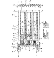
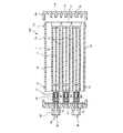
図1は本発明の第1実施形態である電気回路基板収容箱の分解斜視図、図2は図1に示す接続回路部材および蓋部材の分解斜視図、そして図3は図1に示す電気回路基板が収容された電気回路基板収容箱の縦断面図である。
(First embodiment)
1 is an exploded perspective view of an electric circuit board housing box according to a first embodiment of the present invention, FIG. 2 is an exploded perspective view of a connection circuit member and a lid member shown in FIG. 1, and FIG. 3 is an electric circuit shown in FIG. It is a longitudinal cross-sectional view of the electric circuit board | substrate accommodation box in which the board | substrate was accommodated.
図1〜図3に示されるように、本発明に係る電気回路基板収容箱の第1実施形態は、電気回路パターン27が形成されたベースボード29と当該ベースボード29の一端縁29bに沿って該ベースボード29上に配置され且つ電気回路パターン27に電気的に接続するボードコネクタ23とを有する電気回路基板21を複数、積層するように収容可能な電気回路基板収容箱であって、
開口が形成された一側面を有し且つ、ボードコネクタ23それぞれが当該開口から露出されながらベースボード29がそれぞれ間隔をあけて並べられるように複数の電気回路基板21を収容する収容箱本体11と、
ワイヤハーネス51の相手方コネクタ57と電気的に接続可能な入出力端子39を収容するためのコネクタハウジング13fが一体成形された蓋部材13と、
蓋部材13と収容箱本体11とに介在するように蓋部材13に固定され、ボードコネクタ23とそれぞれ嵌合且つ電気的に接続するための複数のコネクタ43を有し、且つ当該コネクタ43と入出力端子39とが電気的に導通する接続回路部材37と、
を具備し、
接続回路部材37のコネクタ43をボードコネクタ23に一括して嵌合させながら蓋部材13が収容箱本体11の開口を覆うように収容箱本体11に取り付けられる。
As shown in FIGS. 1 to 3, the first embodiment of the electric circuit board storage box according to the present invention is along the
An
A
The
Comprising
The
このように構成された電気回路基板収容箱100について以下に詳細に説明する。
The electric circuit
電気回路基板収容箱100は、収容箱本体11と、蓋部材13と、裏蓋15とを有する。収容箱本体11は、上面11a、下面11b、および該上下面11a、11bに連続して形成された左右側壁11c,11dと、を備え、略中空4角柱状に形成されている。収容箱本体11の中空の内部は、複数の仕切り壁11eにより仕切られて、複数の基板収容室17が形成されている。各基板収容室17は、前後方向に貫通しており、外部に開口する。各基板収容室17には、内ケース25に収容された電気回路基板21が収容される。
The electric circuit
ここで、電気回路基板21のボードコネクタ23の挿抜方向を前後方向、これと直交し且つ図3における紙面に垂直方向を左右方向、前後方向および左右方向と直交する方向を上下方向と定義し、以後本明細書においては、これに従って説明する。
Here, the insertion / removal direction of the
収容箱本体11の上下面11a、11bの前方側には、その左右方向略中央に、前後方向中央に向かうに従って次第に高くなる傾斜面を有する断面略3角形の係止突起11fがそれぞれ設けられている。また、収容箱本体11の後方側には、上下面11a、11bの左右方向略中央、および左右側壁11c,11dの上下方向略中央に、係止突起11fと同様の形状を有する断面略3角形の係止突起11gが、それぞれ設けられている。
On the front side of the upper and
電気回路基板21は、電子制御ユニット28が電気的に接続された電気回路パターン27が形成された電気回路パターン面29aを有するベースボード29を備える。電気回路基板21は、ベースボード29の一端縁29bに沿って電気回路パターン面29a上に配置された少なくとも一つのボードコネクタ23を有する。電気回路基板21は、内ケース25に収容されて、それぞれの基板収容室17に積層されるようにそれぞれ間隔をあけて並べられる。尚、第1実施形態におけるボードコネクタ23は、一端がベースボード29のスルーホールに貫通してハンダ付けされ、他端が直角に曲げられてベースボード29と並行に形成された雄接続端子33と、該雄接続端子33を収容する雌ハウジング31とからなり、電気回路基板21と平行にコネクタが挿抜される基板直付け形のアングルコネクタである。
The
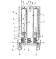
蓋部材13は、収容箱本体11の一方の開口を塞ぐものであり、矩形板状の蓋本体13aと、該蓋本体13aの4辺から立設する上壁13b、下壁13c、左右壁13d,13eを有する有底箱状に形成されている。蓋本体13aには、後述する接続回路部材37の入出力端子39を挿入する貫通穴13gが設けられたフード状のコネクタハウジング(雌コネクタハウジング)13fが、外方に突出して形成されている。上壁13bおよび下壁13cの左右方向略中央には、収容箱本体11の係止突起11fと係合する係止穴35が形成されている。
The
図2に示されるように、蓋部材13の内面には、接続回路部材37が固定される。接続回路部材37の一方の面には、基板収容室17に収容された電気回路基板21のボードコネクタ23に対応して、雌接続端子45を収容したコネクタ43が配設されている。本実施形態のコネクタ43は、雌接続端子45が接続回路部材37に面実装される雄コネクタとなっている。また、接続回路部材37の他方の面には、入出力端子39が配設されている。
As shown in FIG. 2, a
入出力端子39は、その後端が接続回路部材37に設けられたスルーホール41に挿入、ハンダ付けされ、先端が蓋部材13の貫通穴13gに挿入されてコネクタハウジング13f内に突出して配置されている。即ち、コネクタハウジング13fと入出力端子39とにより、入出力コネクタ49が形成され、ワイヤハーネス51に設けられた相手方コネクタ57と嵌合する。各コネクタ43の雌接続端子45は、接続回路部材37に形成された電気回路パターン53によって整理され、或いは統合されて入出力端子39に電気的に接続している。
The input /
裏蓋15は、基板収容室17(収容箱本体11)の後部の開口を塞ぐものであり、開口と略同じ大きさを有する矩形板状蓋部15aと、該矩形板状蓋部15aの4辺から立設された四角枠状の側壁15bを有し、有底箱状に形成されている。矩形板状蓋部15aの内面には、基板収容室17に収容された内ケース25を押さえるための押圧片15cが左右方向に形成されている。また、上部および下部の側壁15bの左右方向略中央、および左右の側壁15bの上下方向略中央には、収容箱本体11の係止突起11gと係合する係合穴55が形成されている。
The
本発明の第1実施形態の電気回路基板収容箱の組付けについて説明する。第1実施形態の電気回路基板収容箱100は、収容箱本体11の後部に裏蓋15を嵌合し、収容箱本体11の係止突起11gと裏蓋15の係合穴55を係合して組み付ける。次に、収容箱本体11の前方の開口から、電気回路基板21が収容された内ケース25を裏蓋15の押圧片15cに当接するまで挿入して、基板収容室17内に収容する。そして、電気回路基板21の各ボードコネクタ23に、接続回路部材37のコネクタ43を嵌合させつつ、蓋部材13を収容箱本体11の前部に嵌合し、収容箱本体11の係止突起11fと蓋部材13の係止穴35を係合して組み付ける。
The assembly of the electric circuit board storage box of the first embodiment of the present invention will be described. In the electric circuit
これにより、基板収容室17に収容された内ケース25、即ち電気回路基板21は、裏蓋15の押圧片15cと接続回路部材37のコネクタ43によって挟持される。また、同時に収容箱本体11の前方の開口は蓋部材13のカバー面である蓋本体13aによって塞がれ、また収容箱本体11の後方の開口は裏蓋15によって塞がれる。これにより、前後に開口を有する収容箱本体11の機械的強度は大幅に向上する。また、電気回路基板21のボードコネクタ23は、コネクタ43、接続回路部材37に形成された電気回路パターン53を介して、入出力コネクタ49の入出力端子39に電気的に接続される。
Thereby, the
電気回路基板収容箱100によれば、収容箱本体11に収容された複数の電気回路基板21のボードコネクタ23に接続回路部材37の複数のコネクタ43を一括して嵌合させながら蓋部材13が収容箱本体11の開口を覆うように収容箱本体11に取り付けられるので、接続作業効率が大幅に向上する。換言すれば、接続すべきコネクタ同士をいちいち探して接続する煩雑な接続作業を行なう必要がなく、コネクタ同士の接続作業が容易となる。更に、コネクタの誤接続、即ち、誤配索を確実に防止することができ、信頼性の高い配索を行なうことができる。その上、収容箱本体11の開口を覆う蓋部材13が、ワイヤハーネス51の相手方コネクタ57と電気的に接続可能な入出力端子39を収容するためのコネクタハウジング13fと一体成形されており、相手方コネクタ57を挿入するための大きな貫通穴は必要ないので、蓋部材13の機械的強度が高い。よって、このような蓋部材13が取り付けられた収容箱本体11は補強される。
According to the electric circuit
また、電気回路基板収容箱100によれば、接続回路部材37に形成された電気回路パターン53により、ボードコネクタ23との接続関係が整理され、或いは統合された入出力端子39が接続回路部材37に設けられているので、入出力コネクタ49の数を低減することができ、ワイヤハーネス51の相手方コネクタ57を入出力コネクタに接続するだけで、複数の電気回路基板21の接続を確実且つ容易に行なうことができる。また、電気回路基板21のパターンが変更されても、接続回路部材37の電気回路パターン53を変更することにより、容易に対応することが可能となる。更に、複数のコネクタ43の雌接続端子45は、接続回路部材37の電気回路パターン53により整理され、或いは統合された状態で入出力端子39に接続されているので、以後のメンテナンスも容易となる。
Further, according to the electric circuit
(変形例)
ここで、本発明に係る電気回路基板収容箱の第1実施形態の変形例について、図4および図5を参照して説明する。図4は変形例の電気回路基板収容箱の分解斜視図、図5は図4に示す接続回路部材および蓋部材の分解斜視図である。尚、変形例の電気回路基板収容箱は、接続回路部材の形態が第1実施形態の電気回路基板収容箱と異なるだけで、他の部分は同様であるので、同一部分には同一符号又は相当符号を付して説明を簡略化又は省略する。
(Modification)
Here, the modification of 1st Embodiment of the electric circuit board | substrate accommodation box which concerns on this invention is demonstrated with reference to FIG. 4 and FIG. FIG. 4 is an exploded perspective view of a modified example of the electric circuit board housing box, and FIG. 5 is an exploded perspective view of the connection circuit member and the lid member shown in FIG. The electric circuit board storage box of the modified example is the same as the electric circuit board storage box of the first embodiment except for the configuration of the connection circuit member, and the other parts are the same. The description is simplified or omitted with reference numerals.
図4および図5に示されるように、本発明に係る電気回路基板収容箱の第1実施形態の変形例は、電気回路パターン27が形成されたベースボード29と当該ベースボード29の一端縁29bに沿って該ベースボード29上に配置され且つ電気回路パターン27に電気的に接続するボードコネクタ23とを有する電気回路基板21を複数、積層するように収容可能な電気回路基板収容箱150であって、
開口が形成された一側面を有し且つ、ボードコネクタ23それぞれが当該開口から露出されながらベースボード29がそれぞれ間隔をあけて並べられるように複数の電気回路基板21を収容する収容箱本体11と、
ワイヤハーネス51の相手方コネクタ57と電気的に接続可能な入出力端子39を収容するためのコネクタハウジング13fが一体成形された蓋部材13と、
蓋部材13と収容箱本体11とに介在するように蓋部材13に固定され、ボードコネクタ23とそれぞれ嵌合且つ電気的に接続するための複数のコネクタ43を有し、且つ当該コネクタ43と入出力端子39とが電気的に導通する接続回路部材151と、
を具備し、
接続回路部材151が、その複数のコネクタ43の接続端子45を収容するコネクタハウジング155eが一体成形された一体ハウジング蓋155を備え、
接続回路部材151のコネクタ43をボードコネクタ23に一括して嵌合させながら一体ハウジング蓋155が収容箱本体11の開口を覆うように収容箱本体11に取り付けられる。
4 and 5, the modification of the first embodiment of the electric circuit board storage box according to the present invention includes a
An
A
The
Comprising
The
The
このように構成された電気回路基板収容箱150について以下に詳細に説明する。
The electric circuit
電気回路基板収容箱150は、収容箱本体11と、蓋部材13と、裏蓋15と、接続回路部材151を有する。収容箱本体11の側壁11c,11dの上下方向略中央には、断面略3角形の係止突起11hが形成されている。接続回路部材151は、接続基板153と一体ハウジング蓋155を備える。接続基板153の一方の面は、基板収容室17に収容された電気回路基板21のボードコネクタ23に対応して、複数の雌接続端子45が配設されている。また、接続基板153の他方の面は、入出力端子39が配設されている。
The electric circuit
一体ハウジング蓋155は、矩形板部155aの四辺に上下壁155b、および左右側壁155cが連続して立設した有底箱状に形成されている。上下壁155bの左右方向略中央には、蓋部材13の係止穴35と係合するための断面略3角形の係止突起155dが形成されている。また、左右側壁155cの上下方向略中央には、収容箱本体11の係止突起11hと係合するための係止穴157が設けられている。矩形板部155aには、基板収容室17に収容された電気回路基板21のボードコネクタ23に対応して、複数のコネクタハウジング155eが突出して形成されており、該コネクタハウジング155eに接続基板153の雌接続端子45を収容して接続基板153と一体ハウジング蓋155が組み付けられる。このように接続回路部材151には、コネクタハウジング155eと雌接続端子45によって構成されたコネクタ43が配設される。
The
このように構成された電気回路基板収容箱150によれば、収容箱本体11に収容された複数の電気回路基板21のボードコネクタ23に接続回路部材151の複数のコネクタ43を一括して嵌合させながら接続回路部材151の一体ハウジング蓋155が収容箱本体11の開口を覆うように収容箱本体11に取り付けられるので、電気回路基板収容箱100と同様に、接続作業効率が大幅に向上する。換言すれば、接続すべきコネクタ同士をいちいち探して接続する煩雑な接続作業を行なう必要がなく、コネクタ同士の接続作業が容易となる。更に、コネクタの誤接続、即ち、誤配索を確実に防止することができ、信頼性の高い配索を行なうことができる。その上、接続回路部材151の一体ハウジング蓋155は、ボードコネクタ23とそれぞれ嵌合且つ電気的に接続するための複数のコネクタ43の接続端子45を収容するコネクタハウジング155eが一体成形された部材であり、相手方コネクタ57を挿入するための大きな貫通穴は必要ないので、一体ハウジング蓋155の機械的強度が高い。従って、このような一体ハウジング蓋が取り付けられた収容箱本体は補強される。
According to the electric circuit
また、接続回路部材151において、ボードコネクタ23と接続するコネクタ43のコネクタハウジング155eが、一体ハウジング蓋155に一体に形成されるので、コネクタ43の相対位置精度が高く、積層された多数の電気回路基板21のボードコネクタ23と確実且つ容易に接続することができる。また仕様の異なる複数個の接続基板153および一体ハウジング蓋155を準備しておき、要求される仕様に合わせて最適な接続基板153および一体ハウジング蓋155を適宜選択して組み立てることにより、多くの仕様の接続回路部材151を最小の接続基板153および一体ハウジング蓋155で構成することができる。
その他の作用や効果については、電気回路基板収容箱100の上記説明から容易に類推可能であるため説明を省略する。
Further, in the
Other operations and effects can be easily inferred from the above description of the electric circuit
(第2実施形態)
次に、電気回路基板収容箱の第2実施形態について図6を参照して説明する。図6は本発明の第2実施形態である電気回路基板収容箱の縦断面図である。
図6に示されるように、第2実施形態の電気回路基板収容箱200は、裏蓋がなく、また収容箱本体121の形状が一部異なる以外は、第1実施形態の電気回路基板収容箱100と同様であるので、同一部分には同一符号又は相当符号を付して説明を簡略化又は省略する。
(Second Embodiment)
Next, a second embodiment of the electric circuit board storage box will be described with reference to FIG. FIG. 6 is a longitudinal sectional view of an electric circuit board storage box according to the second embodiment of the present invention.
As shown in FIG. 6, the electrical circuit
収容箱本体121に形成された各基板収容室17の左右側壁11c,11dの後部は、後端から前方に向かって平行に設けられた2本のスリット123により、上下が側壁11c,11dから分離され、前端だけが側壁11c,11dに連続する弾性片125を備える。弾性片125は、左右方向(図6において紙面に垂直方向)に弾性変形可能であり、その内面には後端から前方に向かうに従って次第に内側に突出する傾斜面125aと該傾斜面125aから側壁11c,11dに直角に形成された係止面125bを有する。
The rear portions of the left and
電気回路基板21が収容された内ケース25を、基板収容室17に前方から挿入すると、内ケース25の後端が係止面125bに当接して基板収容室17内での前後方向位置が位置決めされる。或いは、電気回路基板21が収容された内ケース25を、弾性片125を弾性変形させながら、後方の開口から基板収容室17に挿入するようにしてもよい。この場合、内ケース25の後端が係止面125bに達すると、弾性片125は弾性力により復帰して係止面125bが内ケース25の後端を係止し、以後、内ケース25の後方への移動を阻止する。
When the
電気回路基板収容箱200の他の作用や効果については、第1実施形態の電気回路基板収容箱100の上記説明から容易に類推可能であるため説明を省略する。尚、以下に述べる各実施形態においても同様であるので、特にことわりのない限り説明を省略する。
また、図4および図5において既に説明した変形例への展開、即ち、接続基板と一体ハウジング蓋とにより接続回路部材を構成することは、第2実施形態および以下に述べる各実施形態においても同様に可能であり、上記説明から容易に類推可能であるため説明を省略する。
Other actions and effects of the electric circuit
Further, the development to the modified example already described in FIGS. 4 and 5, that is, the configuration of the connection circuit member by the connection substrate and the integral housing lid is the same in the second embodiment and the embodiments described below. The description is omitted because it can be easily inferred from the above description.
(第3実施形態)
次に、本発明の電気回路基板収容箱の第3実施形態を説明する。図7は本発明の第3実施形態である電気回路基板収容箱の縦断面図である。
図7に示されるように、第3実施形態の電気回路基板収容箱300は、内ケースが使用されておらず、電気回路基板21が直接、収容箱本体131に収容される。収容箱本体131の左右側壁11c,11dの内面には、複数対の突提部131aが水平に形成されている。対を成す突堤部131aの間隔は、電気回路基板21の厚さより僅かに広い幅を有し、溝133が形成される。そして、電気回路基板21は、該溝133に挿入されて収容箱本体131に収容される。
(Third embodiment)
Next, a third embodiment of the electric circuit board storage box of the present invention will be described. FIG. 7 is a longitudinal sectional view of an electric circuit board storage box according to the third embodiment of the present invention.
As shown in FIG. 7, the electric circuit
また、裏蓋135の内面には、電気回路基板21の厚さより僅かに広い幅を有する溝137が水平に設けられた押さえリブ135aが左右方向に形成されている。裏蓋135は、溝137内に電気回路基板21の後端部を挿入して電気回路基板21を支持する。
その他の部分については、本発明の第1実施形態の電気回路基板収容箱100と同様であるので、同一部分には同一符号又は相当符号を付して説明を簡略化又は省略する。
In addition, on the inner surface of the
Since other parts are the same as those of the electric circuit
(第4実施形態)
次に、本発明の電気回路基板収容箱の第4実施形態を説明する。図8は本発明の第4実施形態である電気回路基板収容箱の縦断面図である。
第4実施形態の電気回路基板収容箱400は、接続回路部材37の他方の面に配設された入出力端子141が面実装されている以外は、図3に示された第1実施形態の電気回路基板収容箱100と同様である。入出力端子141は、接続回路部材37の電気回路パターン53に面実装によりハンダ付けされており、蓋部材13の貫通穴13gに挿入されてコネクタハウジング13f内に突出して配置される。これにより、入出力コネクタ49が形成される。
(Fourth embodiment)
Next, a fourth embodiment of the electric circuit board storage box of the present invention will be described. FIG. 8 is a longitudinal sectional view of an electric circuit board storage box according to the fourth embodiment of the present invention.
The electric circuit
(第5実施形態)
次に、本発明の電気回路基板収容箱の第5実施形態を説明する。図9は本発明の第5実施形態である電気回路基板収容箱の縦断面図である。
第5実施形態の電気回路基板収容箱500は、接続回路部材37の他方の面に配設された入出力端子141が面実装されている以外は、図6に示された第2実施形態の電気回路基板収容箱200と同様である。
(Fifth embodiment)
Next, a fifth embodiment of the electric circuit board storage box of the present invention will be described. FIG. 9 is a longitudinal sectional view of an electric circuit board storage box according to the fifth embodiment of the present invention.
The electric circuit
(第6実施形態)
次に、本発明の電気回路基板収容箱の第6実施形態を説明する。図10は本発明の第6実施形態である電気回路基板収容箱の縦断面図である。
第6実施形態の電気回路基板収容箱600は、接続回路部材37の他方の面に配設された入出力端子141が面実装されている以外は、図7に示された第3実施形態の電気回路基板収容箱300と同様である。
(Sixth embodiment)
Next, a sixth embodiment of the electric circuit board storage box of the present invention will be described. FIG. 10 is a longitudinal sectional view of an electric circuit board storage box according to the sixth embodiment of the present invention.
The electric circuit
(第7実施形態)
次に、本発明の電気回路基板収容箱の第7実施形態を説明する。図11は本発明の第7実施形態である電気回路基板収容箱の縦断面図である。
第7実施形態の電気回路基板収容箱700は、電気回路基板21の一端縁29bに沿って電気回路パターン面29a上に配置されたボードコネクタ171の雄接続端子173が電気回路基板21の電気回路パターン27に面実装されてハンダ付けされる面実装タイプのコネクタである以外は、図8に示された第4実施形態の電気回路基板収容箱400と同様である。
(Seventh embodiment)
Next, a seventh embodiment of the electric circuit board storage box of the present invention will be described. FIG. 11 is a longitudinal sectional view of an electric circuit board storage box according to the seventh embodiment of the present invention.
In the electric circuit
(第8実施形態)
次に、本発明の電気回路基板収容箱の第8実施形態を説明する。図12は本発明の第8実施形態である電気回路基板収容箱の縦断面図である。
第8実施形態の電気回路基板収容箱800は、電気回路基板21の一端縁29bに沿って電気回路パターン面29a上に配置されたボードコネクタ171の雄接続端子173が電気回路基板21の電気回路パターン27に面実装されてハンダ付けされる面実装タイプのコネクタである以外は、図9に示された第5実施形態の電気回路基板収容箱500と同様である。
(Eighth embodiment)
Next, an eighth embodiment of the electric circuit board storage box of the present invention will be described. FIG. 12 is a longitudinal sectional view of an electric circuit board storage box according to the eighth embodiment of the present invention.
In the electric circuit
(第9実施形態)
次に、本発明の電気回路基板収容箱の第9実施形態を説明する。図13は本発明の第9実施形態である電気回路基板収容箱の縦断面図である。
第9実施形態の電気回路基板収容箱900は、電気回路基板21の一端縁29bに沿って配置されたボードコネクタ191がオスコネクタであり、該ボードコネクタ191の雌接続端子193が電気回路パターン27に面実装されている。また、接続回路部材37の一方の面に配設されたコネクタ195が雌コネクタであり、該コネクタ195の雄接続端子197は接続回路部材37に面実装されている。その他の部分は、図11に示された第7実施形態の電気回路基板収容箱700と同様である。
(Ninth embodiment)
Next, a ninth embodiment of the electric circuit board storage box of the present invention will be described. FIG. 13 is a longitudinal sectional view of an electric circuit board storage box according to the ninth embodiment of the present invention.
In the electric circuit
(第10実施形態)
次に、本発明の電気回路基板収容箱の第10実施形態を説明する。図14は本発明の第10実施形態である電気回路基板収容箱の縦断面図である。
第10実施形態の電気回路基板収容箱1000は、電気回路基板21にオスコネクタであるボードコネクタ191の雌接続端子193が面実装され、また接続回路部材37の一方の面に雌コネクタであるコネクタ195の雄接続端子197が面実装されている以外は、図12に示される第8実施形態の電気回路基板収容箱800と同様である。
(10th Embodiment)
Next, a tenth embodiment of the electric circuit board storage box of the present invention will be described. FIG. 14 is a longitudinal sectional view of an electric circuit board storage box according to the tenth embodiment of the present invention.
In the electric circuit
(第11実施形態)
次に、本発明の電気回路基板収容箱の第11実施形態を説明する。図15は本発明の第11実施形態である電気回路基板収容箱の縦断面図である。
第11実施形態の電気回路基板収容箱1100は、電気回路基板21にボードコネクタが配設されておらず、電気回路基板21の一端縁29bに沿って電気回路パターン面29aに接続する電気接触部(図示せず)が形成されている。電気接触部は、電気回路基板21の片面に形成されていても、両面に形成されていてもよい。電気回路基板21は、電気接触部、即ち一端縁29bを露出させて内ケース25内に収容されている。また、接続回路部材37の一方の面に配設されたコネクタは、エッジコネクタ113であり、接続端子111が弾性力によって各電気回路基板21の電気接触部にそれぞれ接触して電気的に接続する。
(Eleventh embodiment)
Next, an eleventh embodiment of the electric circuit board storage box of the present invention will be described. FIG. 15 is a longitudinal sectional view of an electric circuit board storage box according to the eleventh embodiment of the present invention.
In the electric circuit
一部のエッジコネクタ113の接続端子111は入出力端子115としての機能も有し、蓋部材13に形成された貫通穴13gに挿入されてコネクタハウジング13fに収容されて入出力コネクタ49が形成される。蓋部材13の貫通穴13gに挿入されず、電気回路基板21の電気接触部にのみ接触する接続端子111(図15において中段に配置されたエッジコネクタ113の接続端子111)は、接続回路部材37の電気回路パターン53によって整理され、或いは統合されて入出力コネクタ49の入出力端子115に接続されている。
その他の部分は、図3に示される第1実施形態の電気回路基板収容箱100と同様であるので同一部分には同一符号又は相当符号を付して説明を簡略化又は省略する。
The
The other parts are the same as those of the electric circuit
(第12実施形態)
次に、本発明の電気回路基板収容箱の第12実施形態を説明する。図16は本発明の第12実施形態である電気回路基板収容箱の縦断面図である。
第12実施形態の電気回路基板収容箱1200は、第11実施形態の電気回路基板収容箱1100と同様に電気回路基板21に形成された電気接触部およびエッジコネクタ113を有しており、その他の部分は、図6に示される第2実施形態の電気回路基板収容箱200と同様であるので詳細な説明は省略する。
(Twelfth embodiment)
Next, a twelfth embodiment of the electric circuit board storage box of the present invention will be described. FIG. 16 is a longitudinal sectional view of an electric circuit board storage box according to the twelfth embodiment of the present invention.
The electric circuit
(第13実施形態)
次に、本発明の電気回路基板収容箱の第13実施形態を説明する。図17は本発明の第13実施形態である電気回路基板収容箱の縦断面図である。
第13実施形態の電気回路基板収容箱1300は、第11実施形態の電気回路基板収容箱1100と同様に電気回路基板21に形成された電気接触部およびエッジコネクタ113を有しており、その他の部分は、図7に示される第3実施形態の電気回路基板収容箱300と同様であるので詳細な説明は省略する。
(13th Embodiment)
Next, a thirteenth embodiment of the electric circuit board storage box of the present invention will be described. FIG. 17 is a longitudinal sectional view of an electric circuit board storage box according to a thirteenth embodiment of the present invention.
The electric circuit
尚、本発明は、前述した実施形態および変形例に限定されるものではなく、適宜、変形、改良、等が可能である。その他、前述した実施形態および変形例における各構成要素の材質、形状、寸法、数値、形態、数、配置箇所、等は本発明を達成できるものであれば任意であり、限定されない。 Note that the present invention is not limited to the above-described embodiments and modifications, and modifications, improvements, and the like can be made as appropriate. In addition, the material, shape, dimension, numerical value, form, number, arrangement location, and the like of each component in the embodiment and the modification described above are arbitrary and are not limited as long as the present invention can be achieved.
100 電気回路基板収容箱
150 電気回路基板収容箱
11 収容箱本体
13 蓋部材
13a 蓋本体
13f コネクタハウジング
21 電気回路基板
23 ボードコネクタ
27 電気回路パターン
29 ベースボード
29a 電気回路パターン面
29b 一端縁
37 接続回路部材
39 入出力端子
43 コネクタ
45 接続端子
51 ワイヤハーネス
53 電気回路パターン
57 相手方コネクタ
151 接続回路部材
153 接続基板
155 一体ハウジング蓋
155e コネクタハウジング
DESCRIPTION OF
Claims (2)
開口が形成された一側面を有し且つ、前記ボードコネクタそれぞれが前記開口から露出されながら前記ベースボードがそれぞれ間隔をあけて並べられるように複数の前記電気回路基板を収容する収容箱本体と、
ワイヤハーネスの相手方コネクタと電気的に接続可能な入出力端子を収容するためのコネクタハウジングが一体成形された蓋部材と、
前記蓋部材と前記収容箱本体とに介在するように前記蓋部材に固定され、前記ボードコネクタとそれぞれ嵌合且つ電気的に接続するための複数のコネクタを有し、且つ当該コネクタと前記入出力端子とが電気的に導通する接続回路部材と、
を具備し、
前記接続回路部材の前記コネクタを前記ボードコネクタに一括して嵌合させながら前記蓋部材が前記収容箱本体の前記開口を覆うように前記収容箱本体に取り付けられることを特徴とする電気回路基板収容箱。 A plurality of electric circuit boards having a base board on which an electric circuit pattern is formed and a board connector disposed on the base board along one edge of the base board and electrically connected to the electric circuit pattern are stacked. An electric circuit board storage box that can be stored as follows:
An accommodation box body that accommodates a plurality of the electric circuit boards so that the base boards are arranged at intervals while each of the board connectors is exposed from the opening;
A lid member integrally formed with a connector housing for accommodating an input / output terminal that can be electrically connected to the mating connector of the wire harness;
A plurality of connectors that are fixed to the lid member so as to be interposed between the lid member and the housing main body, and are respectively fitted and electrically connected to the board connector; and the connector and the input / output A connection circuit member electrically connected to the terminal;
Comprising
An electrical circuit board housing, wherein the lid member is attached to the housing box body so as to cover the opening of the housing body while the connectors of the connection circuit member are collectively fitted to the board connector. box.
開口が形成された一側面を有し且つ、前記ボードコネクタそれぞれが前記開口から露出されながら前記ベースボードがそれぞれ間隔をあけて並べられるように複数の前記電気回路基板を収容する収容箱本体と、
ワイヤハーネスの相手方コネクタと電気的に接続可能な入出力端子を収容するためのコネクタハウジングが形成された蓋部材と、
前記蓋部材と前記収容箱本体とに介在するように前記蓋部材に固定され、前記ボードコネクタとそれぞれ嵌合且つ電気的に接続するための複数のコネクタを有し、且つ当該コネクタと前記入出力端子とが電気的に導通する接続回路部材と、
を具備し、
前記接続回路部材が、その前記複数のコネクタの接続端子を収容するコネクタハウジングが一体成形された一体ハウジング蓋を備え、
前記接続回路部材の前記コネクタを前記ボードコネクタに一括して嵌合させながら前記一体ハウジング蓋が前記収容箱本体の前記開口を覆うように前記収容箱本体に取り付けられることを特徴とする電気回路基板収容箱。 A plurality of electric circuit boards having a base board on which an electric circuit pattern is formed and a board connector disposed on the base board along one edge of the base board and electrically connected to the electric circuit pattern are stacked. An electric circuit board storage box that can be stored as follows:
An accommodation box body that accommodates a plurality of the electric circuit boards so that the base boards are arranged at intervals while each of the board connectors is exposed from the opening;
A lid member formed with a connector housing for accommodating an input / output terminal that can be electrically connected to the mating connector of the wire harness;
A plurality of connectors that are fixed to the lid member so as to be interposed between the lid member and the housing main body, and are respectively fitted and electrically connected to the board connector; and the connector and the input / output A connection circuit member electrically connected to the terminal;
Comprising
The connection circuit member includes an integral housing lid integrally formed with a connector housing that accommodates connection terminals of the plurality of connectors;
The electric circuit board, wherein the integrated housing cover is attached to the housing box body so as to cover the opening of the housing box body while the connectors of the connection circuit members are collectively fitted to the board connector. Containment box.
Priority Applications (3)
| Application Number | Priority Date | Filing Date | Title |
|---|---|---|---|
| JP2005083952A JP4408826B2 (en) | 2005-03-23 | 2005-03-23 | Electrical circuit board storage box |
| US11/385,865 US20060216965A1 (en) | 2005-03-23 | 2006-03-22 | Receiving box |
| DE102006013525A DE102006013525A1 (en) | 2005-03-23 | 2006-03-23 | receiving housing |
Applications Claiming Priority (1)
| Application Number | Priority Date | Filing Date | Title |
|---|---|---|---|
| JP2005083952A JP4408826B2 (en) | 2005-03-23 | 2005-03-23 | Electrical circuit board storage box |
Publications (2)
| Publication Number | Publication Date |
|---|---|
| JP2006269632A true JP2006269632A (en) | 2006-10-05 |
| JP4408826B2 JP4408826B2 (en) | 2010-02-03 |
Family
ID=36999140
Family Applications (1)
| Application Number | Title | Priority Date | Filing Date |
|---|---|---|---|
| JP2005083952A Expired - Fee Related JP4408826B2 (en) | 2005-03-23 | 2005-03-23 | Electrical circuit board storage box |
Country Status (3)
| Country | Link |
|---|---|
| US (1) | US20060216965A1 (en) |
| JP (1) | JP4408826B2 (en) |
| DE (1) | DE102006013525A1 (en) |
Cited By (4)
| Publication number | Priority date | Publication date | Assignee | Title |
|---|---|---|---|---|
| JP2010182673A (en) * | 2009-02-06 | 2010-08-19 | Tyco Electronics Corp | End cap assembly |
| JP2011028856A (en) * | 2009-07-21 | 2011-02-10 | Denso Corp | Electronic device |
| JP2011210458A (en) * | 2010-03-29 | 2011-10-20 | Autonetworks Technologies Ltd | Electronic circuit unit which can achieve external connection |
| WO2018155691A1 (en) | 2017-02-27 | 2018-08-30 | 川崎重工業株式会社 | Casing and method for mounting substrate to casing |
Families Citing this family (17)
| Publication number | Priority date | Publication date | Assignee | Title |
|---|---|---|---|---|
| JP5088811B2 (en) * | 2007-01-10 | 2012-12-05 | 矢崎総業株式会社 | Electrical junction box |
| US7511967B2 (en) * | 2007-02-20 | 2009-03-31 | United Technologies Corporation | Avionics enclosure |
| JP4969364B2 (en) * | 2007-08-13 | 2012-07-04 | 株式会社ニフコ | Mounting structure |
| DE102010025085A1 (en) * | 2010-06-25 | 2011-12-29 | Continental Automotive Gmbh | Control device e.g. electrical control device, for motor car to control e.g. vehicle functions, has circuitry carriers designed such that electrical contact is arranged between contacting unit and one of circuitry carriers |
| DE102011076373B4 (en) | 2011-05-24 | 2024-02-15 | Bayerische Motoren Werke Aktiengesellschaft | Electrical control unit for vehicles |
| DE202013101369U1 (en) * | 2013-03-28 | 2013-04-12 | Waldemar Marinitsch | Housing for driver assistance systems |
| US9173304B2 (en) | 2013-07-18 | 2015-10-27 | Lenovo Enterprise Solutions (Singapore) Pte. Ltd. | Vertical blindmate scaling of identical system boards |
| CN104219915A (en) * | 2014-09-15 | 2014-12-17 | 国核电站运行服务技术有限公司 | Modularized human-computer interaction data acquisition terminal |
| CN105451499B (en) * | 2015-12-11 | 2018-03-30 | 中国航空工业集团公司西安航空计算技术研究所 | A kind of density three-dimensional stack assembly method of electronic module |
| JP6673888B2 (en) * | 2017-10-31 | 2020-03-25 | ファナック株式会社 | Control device |
| KR102030824B1 (en) * | 2017-11-01 | 2019-10-10 | 현대오트론 주식회사 | Electronic control device |
| DE102019002350B3 (en) * | 2019-03-29 | 2020-06-10 | Sinn Power Gmbh | MODULAR ELECTRONIC HOUSING CONCEPT |
| US11412626B2 (en) * | 2019-05-10 | 2022-08-09 | Volvo Truck Corporation | System for arranging ECUs in a chassis of a vehicle |
| TWI764177B (en) * | 2020-06-19 | 2022-05-11 | 仁寶電腦工業股份有限公司 | Fixing device |
| CN114423152B (en) * | 2021-12-31 | 2022-11-04 | 广州弘高科技股份有限公司 | Device with corrosion-resistant multilayer through-hole circuit board |
| DE102022203151A1 (en) * | 2022-03-31 | 2023-10-05 | Robert Bosch Gesellschaft mit beschränkter Haftung | Device with replaceable electronic components of a motor vehicle |
| DE102022207306A1 (en) | 2022-07-18 | 2024-01-18 | Robert Bosch Gesellschaft mit beschränkter Haftung | Device for holding replaceable electronic components of a motor vehicle |
Family Cites Families (2)
| Publication number | Priority date | Publication date | Assignee | Title |
|---|---|---|---|---|
| US5652695A (en) * | 1995-05-05 | 1997-07-29 | Dell Usa, L.P. | Hard drive carrier design permitting floating retention of a connector assembly to facilitate blind mating of the connector assembly in a hard drive bay |
| US5764487A (en) * | 1996-08-06 | 1998-06-09 | Yazaki Corporation | Junction block with integral printed circuit board and electrical connector for same |
-
2005
- 2005-03-23 JP JP2005083952A patent/JP4408826B2/en not_active Expired - Fee Related
-
2006
- 2006-03-22 US US11/385,865 patent/US20060216965A1/en not_active Abandoned
- 2006-03-23 DE DE102006013525A patent/DE102006013525A1/en not_active Withdrawn
Cited By (6)
| Publication number | Priority date | Publication date | Assignee | Title |
|---|---|---|---|---|
| JP2010182673A (en) * | 2009-02-06 | 2010-08-19 | Tyco Electronics Corp | End cap assembly |
| JP2011028856A (en) * | 2009-07-21 | 2011-02-10 | Denso Corp | Electronic device |
| JP2011210458A (en) * | 2010-03-29 | 2011-10-20 | Autonetworks Technologies Ltd | Electronic circuit unit which can achieve external connection |
| WO2018155691A1 (en) | 2017-02-27 | 2018-08-30 | 川崎重工業株式会社 | Casing and method for mounting substrate to casing |
| KR20190112790A (en) | 2017-02-27 | 2019-10-07 | 카와사키 주코교 카부시키 카이샤 | Installation method to casing and casing of board |
| US11013135B2 (en) | 2017-02-27 | 2021-05-18 | Kawasaki Jukogyo Kabushiki Kaisha | Casing and method for mounting substrate to casing |
Also Published As
| Publication number | Publication date |
|---|---|
| JP4408826B2 (en) | 2010-02-03 |
| US20060216965A1 (en) | 2006-09-28 |
| DE102006013525A1 (en) | 2006-10-05 |
Similar Documents
| Publication | Publication Date | Title |
|---|---|---|
| JP4408826B2 (en) | Electrical circuit board storage box | |
| US5822189A (en) | Electrical connection box, a connection construction, a busbar fixing construction and a connection terminal | |
| JP5333849B2 (en) | Electrical junction box | |
| US7699622B2 (en) | Electronic unit and assembling method thereof | |
| US6919509B2 (en) | Electrical junction box | |
| JP5423700B2 (en) | Case for electronic unit and method for manufacturing electronic unit | |
| US6835073B2 (en) | Junction box | |
| JP5149071B2 (en) | Power distribution structure for electrical junction box | |
| JP2009171763A (en) | Electrical junction box | |
| WO2015098482A1 (en) | Electric circuit device | |
| JP2019153572A (en) | Bus bar holding structure, electric connection box, and wire harness | |
| CN108174621B (en) | Connector unit, connector incorporating electrical component, and electrical component with connector | |
| JP2011165348A (en) | Connection structure of wire harness and printed circuit board | |
| JPH1141752A (en) | Electrical junction box | |
| JP2019050660A (en) | Electric connection box and wiring harness | |
| JP2022109562A (en) | Substrate unit, and method of manufacturing the same | |
| JP4250025B2 (en) | Reinforcement structure of electrical junction box | |
| KR20120018843A (en) | Junction box for vehicle | |
| JP2006286464A (en) | Substrate side edge insertion connector | |
| JPH07245155A (en) | Electronic unit installing structure | |
| JP5088946B2 (en) | Junction box | |
| JP2018068022A (en) | Fuse module | |
| JP2007227404A (en) | Joint connector | |
| JP2023045158A (en) | Connection member and electric connection box | |
| JP5381601B2 (en) | Electronic unit configuration module and electronic unit |
Legal Events
| Date | Code | Title | Description |
|---|---|---|---|
| A621 | Written request for application examination |
Free format text: JAPANESE INTERMEDIATE CODE: A621 Effective date: 20070924 |
|
| RD04 | Notification of resignation of power of attorney |
Free format text: JAPANESE INTERMEDIATE CODE: A7424 Effective date: 20071129 |
|
| A977 | Report on retrieval |
Free format text: JAPANESE INTERMEDIATE CODE: A971007 Effective date: 20091021 |
|
| TRDD | Decision of grant or rejection written | ||
| A01 | Written decision to grant a patent or to grant a registration (utility model) |
Free format text: JAPANESE INTERMEDIATE CODE: A01 Effective date: 20091104 |
|
| A01 | Written decision to grant a patent or to grant a registration (utility model) |
Free format text: JAPANESE INTERMEDIATE CODE: A01 |
|
| A61 | First payment of annual fees (during grant procedure) |
Free format text: JAPANESE INTERMEDIATE CODE: A61 Effective date: 20091110 |
|
| R150 | Certificate of patent or registration of utility model |
Ref document number: 4408826 Country of ref document: JP Free format text: JAPANESE INTERMEDIATE CODE: R150 |
|
| FPAY | Renewal fee payment (event date is renewal date of database) |
Free format text: PAYMENT UNTIL: 20121120 Year of fee payment: 3 |
|
| FPAY | Renewal fee payment (event date is renewal date of database) |
Free format text: PAYMENT UNTIL: 20121120 Year of fee payment: 3 |
|
| FPAY | Renewal fee payment (event date is renewal date of database) |
Free format text: PAYMENT UNTIL: 20131120 Year of fee payment: 4 |
|
| R250 | Receipt of annual fees |
Free format text: JAPANESE INTERMEDIATE CODE: R250 |
|
| R250 | Receipt of annual fees |
Free format text: JAPANESE INTERMEDIATE CODE: R250 |
|
| R250 | Receipt of annual fees |
Free format text: JAPANESE INTERMEDIATE CODE: R250 |
|
| R250 | Receipt of annual fees |
Free format text: JAPANESE INTERMEDIATE CODE: R250 |
|
| R250 | Receipt of annual fees |
Free format text: JAPANESE INTERMEDIATE CODE: R250 |
|
| LAPS | Cancellation because of no payment of annual fees |