JP2006221908A - Trigger switch circuit - Google Patents
Trigger switch circuit Download PDFInfo
- Publication number
- JP2006221908A JP2006221908A JP2005032943A JP2005032943A JP2006221908A JP 2006221908 A JP2006221908 A JP 2006221908A JP 2005032943 A JP2005032943 A JP 2005032943A JP 2005032943 A JP2005032943 A JP 2005032943A JP 2006221908 A JP2006221908 A JP 2006221908A
- Authority
- JP
- Japan
- Prior art keywords
- switch
- contact
- trigger
- motor
- circuit
- Prior art date
- Legal status (The legal status is an assumption and is not a legal conclusion. Google has not performed a legal analysis and makes no representation as to the accuracy of the status listed.)
- Granted
Links
Images


Abstract
Description
本発明は電動ドリル等の電動工具に搭載されているトリガースイッチ回路に関するものであり、詳しくはトリガースイッチ回路内の特に電源用スイッチと短絡用スイッチの接点磨耗を削減させるようにし、又、同工具に搭載されている発光手段であるLEDを電動工具のモータが回転する前に点灯するようにした回路構成を有する電動工具のトリガースイッチ回路に関する。 The present invention relates to a trigger switch circuit mounted on an electric tool such as an electric drill, and more particularly, to reduce contact wear of a power switch and a short-circuit switch in the trigger switch circuit. The present invention relates to a trigger switch circuit of an electric tool having a circuit configuration in which an LED, which is a light emitting means, is lit before a motor of the electric tool rotates.
従来のトリガースイッチ回路は、電動工具のトリガーを引き込むことで電源用スイッチをオンにしてモータや摺動回路基板に電源を供給し、モータが高速回転時においては短絡スイッチをオンにしてモータへの電源供給をスイッチング素子を経由しないで直接制御することで高速回転を維持するというものであり、その回路は、図24に示すように、摺動回路基板PCBと、スイッチング素子FETと、モータMと、還流用ダイオードD1と、短絡用スイッチSW−Aと、電源用スイッチSW−Bと、電源Eと、発光ダイオードLEDと、抵抗Rとから構成され、これらは次に示すように接続されている。 The conventional trigger switch circuit turns on the power switch by pulling the trigger of the electric tool and supplies power to the motor and sliding circuit board. When the motor rotates at high speed, the short-circuit switch is turned on and the motor is connected to the motor. The high-speed rotation is maintained by directly controlling the power supply without passing through the switching element. As shown in FIG. 24, the circuit includes a sliding circuit board PCB, a switching element FET, a motor M, The return diode D1, the short-circuit switch SW-A, the power switch SW-B, the power source E, the light-emitting diode LED, and the resistor R are connected as shown below. .
摺動回路基板PCBの端子V+と端子V−との間に直列にモータM、スイッチング素子FETを接続し、これらと並列に直列接続のダイオードD1及び短絡用スイッチSW−Aを接続し、やはり直列接続のモータM、スイッチング素子FETに並列に、直列に電源E及び電源用スイッチSW−B並びにモータブレーキ用スイッチSW−Dを接続した構成になっている。端子V+と端子V−の間には直列接続の発光ダイオードLED、抵抗Rを備えた構成になっている。電源用スイッチSW−B及び短絡用スイッチSW−A、モータブレーキ用スイッチSW−Dは図示しない操作レバーに連動してオン/オフする構成になっている。 A motor M and a switching element FET are connected in series between a terminal V + and a terminal V− of the sliding circuit board PCB, and a series-connected diode D1 and a short-circuit switch SW-A are connected in parallel to these terminals. A power source E, a power switch SW-B, and a motor brake switch SW-D are connected in series to the connected motor M and the switching element FET. Between the terminal V + and the terminal V−, a light emitting diode LED and a resistor R connected in series are provided. The power switch SW-B, the short-circuit switch SW-A, and the motor brake switch SW-D are configured to be turned on / off in conjunction with an operation lever (not shown).
このような構成からなるスイッチの動作について説明すると、先ず、操作レバーがオフの状態のときはモータブレーキ用スイッチSW−Dがオンされ、モータMが短絡し、ブレーキがかかる。そして、操作レバーが引かれると、モータブレーキ用スイッチSW−Dがオフし、電源用スイッチSW−Bがオンになり、電源Eが摺動回路基板PCB、モータM、及び発光ダイオードLEDに供給される。
更に、操作レバーが引かれるとモータMの回転速度が増すように制御され、短絡用スイッチSW−AをオンにしてモータMを高速回転に維持する。
The operation of the switch having such a configuration will be described. First, when the operation lever is in the off state, the motor brake switch SW-D is turned on, the motor M is short-circuited, and the brake is applied. When the operation lever is pulled, the motor brake switch SW-D is turned off, the power switch SW-B is turned on, and the power E is supplied to the sliding circuit board PCB, the motor M, and the light emitting diode LED. The
Further, when the operating lever is pulled, the motor M is controlled to increase its rotational speed, and the short-circuit switch SW-A is turned on to keep the motor M rotating at high speed.
図25は、操作レバーの引き込みに連動して動く摺動子SLDに基づくモータMの回転制御をするためのスイッチ回路を示したものであり、三角波発振回路、電源Eに接続されている端子V+と端子V−との間に直列接続したスイッチSW―C、抵抗R5、抵抗R6、抵抗R7を備え、抵抗R6、R7に並列に直列接続の可変接触子VR1、スイッチSW―Dを配設し、可変接触子VR1と摺動接触子CNTに跨ぐように摺動子SLDを備えた構成になっており、摺動接触子CNTはコンパレータCOMPのマイナス側入力端子に接続されている。スイッチSW―Cは抵抗R5と抵抗R12を切替え、スイッチSW―Dは短絡することで高速回転数を可変にする。
コンパレータCOMPのプラス側入力端子は三角波発振回路の三角波信号を入力する。コンパレータCOMPの出力端子は端子Gに接続され、スイッチング素子FETのゲートに接続されている。
FIG. 25 shows a switch circuit for controlling the rotation of the motor M based on the slider SLD that moves in conjunction with the pulling of the operation lever. The terminal V + connected to the triangular wave oscillation circuit and the power source E is shown in FIG. A switch SW-C, a resistor R5, a resistor R6, and a resistor R7 connected in series between the switch V- and a terminal V-, and a variable contact VR1 and a switch SW-D connected in series in parallel with the resistors R6 and R7. The slider SLD is provided so as to straddle the variable contact VR1 and the sliding contact CNT, and the sliding contact CNT is connected to the negative input terminal of the comparator COMP. The switch SW-C switches between the resistor R5 and the resistor R12, and the switch SW-D is short-circuited to make the high-speed rotation speed variable.
The positive side input terminal of the comparator COMP inputs the triangular wave signal of the triangular wave oscillation circuit. The output terminal of the comparator COMP is connected to the terminal G, and is connected to the gate of the switching element FET.
このような構成の操作レバーに連動して動く摺動子SLDに基づくモータMの回転制御は、先ず、操作レバーが引き込まれ摺動子SLDがBの位置にきたときにモータMの回転は高速になり、このとき高速回転数を可変にするために、スイッチSW―Cを切替、且つスイッチSW―Dをオンにして短絡させることで高速回転を可変にすることができる。
しかしながら、従来技術で説明した電動工具用トリガースイッチ回路は電源用スイッチ及び短絡用スイッチをオン/オフする時に、常にスイッチング素子FETは制御可能な状態になっている。従って、電源用スイッチ又は短絡用スイッチがオン/オフする際にはスイッチング素子FETがオン/オフ制御されているため電源用スイッチ或は短絡用スイッチの接点間に電位差が生じ、電源用スイッチ或は短絡用スイッチのオン/オフ時にスパークが発生することで接点磨耗が多くなり寿命向上が期待できないという問題がある。
又、従来技術における電動工具用トリガースイッチ回路は、電源用スイッチのオンに伴い電動工具のモータ回転とLED点灯が同時に行われているため、電動工具のモータが回転する前にLEDを点灯させるためには電源用スイッチの他にそれと別の独立した補助スイッチを追加する必要があり、これが部品追加に伴う価格の向上をきたし、加えてこの部品追加が大幅な占有面積を占めるという問題がある。
更に、高速回転に制御するためには、複数のスイッチをオンにする必要があり、そのぶん回路が複雑で且つコストも高くつくという問題がある。
従って、電源用スイッチ或は短絡用スイッチをオン/オフするときにスイッチング素子FETをオン/オフ制御しないようにしてスイッチの接点間の電位差をなくすようにすると共に、モータが回転する前にLEDの点灯を行うように制御することで目的とする加工対象物への照射が加工前に照射できるようにすること、並びに、高速回転に制御するときに簡単な手法で行うことができるようにすることに解決しなければならない課題を有する。
However, in the trigger switch circuit for an electric tool described in the prior art, the switching element FET is always in a controllable state when the power switch and the short-circuit switch are turned on / off. Therefore, when the power switch or the shorting switch is turned on / off, the switching element FET is controlled to be turned on / off, so that a potential difference is generated between the contacts of the power switch or the shorting switch. There is a problem that contact wear increases due to the occurrence of sparks when the shorting switch is turned on / off, and the life cannot be improved.
In addition, the trigger switch circuit for the electric tool in the prior art is for turning on the LED before the motor of the electric tool rotates because the motor rotation of the electric tool and the LED lighting are performed at the same time as the power switch is turned on. In addition to the power switch, it is necessary to add another independent auxiliary switch, which raises the price associated with the addition of components, and in addition, this component occupies a large occupied area.
Furthermore, in order to control the rotation at a high speed, it is necessary to turn on a plurality of switches, and there is a problem that the circuit is complicated and expensive.
Therefore, when the power switch or the short-circuit switch is turned on / off, the switching element FET is not controlled to be turned on / off so that the potential difference between the contact points of the switch is eliminated, and the LED is turned on before the motor rotates. By controlling to turn on the light, it is possible to irradiate the target processing object before processing, and to be able to perform by a simple method when controlling to high speed rotation There are problems that must be solved.
上記課題を解決するために、本願発明のトリガースイッチ回路は、次に示す構成にすることである。 In order to solve the above problems, the trigger switch circuit of the present invention is configured as follows.
(1)トリガースイッチ回路は、直流電源とモータ間に設けた電源用スイッチと、前記モータと直列に接続したスイッチング素子と、前記スイッチング素子に並列に接続した短絡用スイッチと、モータを停止させるモータブレーキスイッチと、前記スイッチング素子を駆動させる駆動部と、トリガーが引き込まれたときに前記スイッチング素子のゲートに電圧を供給する制御スイッチと、トリガーを引き込んだときに直流電源を前記駆動部に供給する補助スイッチと、を具備するトリガースイッチ回路であって、前記電源用スイッチと、前記短絡用スイッチと、前記モータブレーキスイッチと、前記制御スイッチと、前記補助スイッチの五者を前記トリガーと連動して動作する構成にし、前記トリガーが引き込まれたときに、前記補助スイッチをオンにして前記駆動部に電源を供給し、更に、トリガーが引き込まれたときに、前記電源用スイッチをオンに制御して前記モータに電源を供給し、更に、トリガーが引き込まれたときに、前記制御スイッチをオンに制御して抵抗を介した電圧を前記スイッチング素子のゲートに供給するように制御し、更に、トリガーが引き込まれたときに、前記制御スイッチのオン状態を直流電源を直接供給する位置にして、前記スイッチング素子のゲートに直流電源を直接供給することで、前記スイッチング素子を100%導通できる状態にし、更に、トリガーを引き込むことで、前記短絡スイッチをオンに制御するようにしたことである。
(2)前記補助スイッチがオンしたときに、発光手段に電源を供給するようにしたことを特徴とする(1)に記載のトリガースイッチ回路。
(3)前記補助スイッチと制御スイッチを構成する摺動子は一つのスイッチ摺動子を用いたことを特徴とする(1)に記載のトリガースイッチ回路。
(4)トリガースイッチ回路は、基準信号を出力する基準信号出力手段と、操作レバーの操作具合に基づいて所定の操作信号を出力する操作信号出力手段と、モータと直列に接続され、モータの回転制御をするスイッチング素子と、前記基準信号出力手段からの基準信号を一方の入力端子に入力し、前記操作信号出力手段からの操作信号を他方の入力端子に入力し、その入力された信号を比較して所定の制御信号を前記スイッチング素子に供給してスイッチング素子をオン/オフ制御するコンパレータと、を備えたトリガースイッチ回路であって、前記操作信号出力手段は、電源と接地間に直列に抵抗Ra、可変抵抗Rc、抵抗Reを接続し、前記可変抵抗Rcに並列に抵抗Rbを接続し、可変接触子72と摺動接触子71を跨いで電気的に接続する回転制御摺動子22aを備え、前記可変接触子72の開始位置と回転制御摺動子22aに接続されている抵抗Rdの出力側の間に高速回転用のスイッチSW5を備えたことである。
(1) A trigger switch circuit includes a power switch provided between a DC power supply and a motor, a switching element connected in series with the motor, a short-circuit switch connected in parallel to the switching element, and a motor for stopping the motor. A brake switch, a drive unit that drives the switching element, a control switch that supplies a voltage to the gate of the switching element when a trigger is pulled, and a DC power supply that is supplied to the drive unit when the trigger is pulled A trigger switch circuit comprising an auxiliary switch, wherein the power switch, the short-circuit switch, the motor brake switch, the control switch, and the auxiliary switch are linked with the trigger. When the trigger is retracted, the auxiliary switch is configured to operate. When the trigger is pulled in, the power switch is turned on, the power switch is turned on to supply power to the motor, and when the trigger is pulled The control switch is controlled to be turned on so that a voltage via a resistor is supplied to the gate of the switching element. Further, when the trigger is pulled, the control switch is turned on by directly connecting the DC power supply. In the position to supply, direct power supply is directly supplied to the gate of the switching element so that the switching element can be made 100% conductive, and further, the trigger is pulled in so that the short-circuit switch is turned on. It is that.
(2) The trigger switch circuit according to (1), wherein power is supplied to the light emitting means when the auxiliary switch is turned on.
(3) The trigger switch circuit according to (1), wherein the switch constituting the auxiliary switch and the control switch uses a single switch slider.
(4) The trigger switch circuit is connected in series with the reference signal output means for outputting the reference signal, the operation signal output means for outputting a predetermined operation signal based on the operation condition of the operation lever, and the rotation of the motor. The switching element to be controlled and the reference signal from the reference signal output means are input to one input terminal, the operation signal from the operation signal output means is input to the other input terminal, and the input signals are compared. And a comparator for supplying a predetermined control signal to the switching element to control on / off of the switching element, wherein the operation signal output means is a resistor in series between the power source and the ground. Ra, a variable resistor Rc, and a resistor Re are connected, a resistor Rb is connected in parallel to the variable resistor Rc, and electrically across the
本発明により、スイッチング素子を遮断状態のときに電源用スイッチをオンし、スイッチング素子が100%導通した状態のときに短絡用スイッチをオンするようにしたため、スイッチに電位差をなくした状態でオンできるため、両スイッチの接点間に発生するスパークを極めて少なくすることができ、接点の寿命を延ばすことができる。
又、モータが回転する前にLEDを点灯できるようにしたことで、電動工具に使用した場合、モータが回転する前にLEDがオンし、被切削物に照射させることが出来るため、位置決め等の使い勝手がよくなるという効果がある。
更に、1個のスイッチSW5のオン/オフだけで高速回転数を設定することができるため電動工具への取付け性が向上するとともにスイッチ1個分のコストダウンも可能になり、又、摺動回路基板の配線も簡略化できるためスイッチ組立て工数の削減も可能となる。
According to the present invention, the power supply switch is turned on when the switching element is in the cut-off state, and the short-circuit switch is turned on when the switching element is 100% conductive, so that the switch can be turned on without any potential difference. Therefore, the spark generated between the contacts of both switches can be extremely reduced, and the life of the contacts can be extended.
In addition, since the LED can be lit before the motor rotates, when used in an electric tool, the LED can be turned on before the motor rotates to irradiate the workpiece. There is an effect that usability is improved.
Furthermore, since the high-speed rotation speed can be set only by turning on / off one switch SW5, the attachment to the electric tool is improved and the cost for one switch can be reduced. Since the wiring of the board can be simplified, it is possible to reduce the number of switch assembly steps.
本願発明に係るトリガースイッチ回路の実施形態について、図面を参照して説明する。 An embodiment of a trigger switch circuit according to the present invention will be described with reference to the drawings.
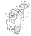
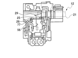
本発明に係るトリガースイッチ回路を備えたトリガースイッチは、図1及び図2に示すように、縦長の箱形状に形成され内部にスイッチ機構を組み込み、外部の操作部11からの操作動作を伝達する摺動操作子12を上部位置に備え、且つ側面を開口にしたケース13と、ケース13の側面の開口面を塞ぐと共に、内側壁面に摺動回路基板を搭載し、外側に制御素子(FET)14を配置するFET配置部16を備えたカバー17と、手の指で操作できる操作部11と、ケース13の頂面に位置しモータの回転切替えをする切替操作部18と、ケース13にカバー17をしたその外周位置に配置した略コ字型形状に形成した放熱板19とを備えた構成になっている。
As shown in FIGS. 1 and 2, the trigger switch including the trigger switch circuit according to the present invention is formed in a vertically long box shape, incorporates a switch mechanism therein, and transmits an operation operation from the
摺動操作子12は、所謂、スイッチ機構を形成するもので、操作部11の操作により、モータへの電源の供給を可能にすること、操作部11の操作具合に応じてモータの速度を制御すること、操作部11の操作具合によりモータへの電源を短絡して供給すること、及びモータ停止時にモータを短絡することの4つの機能を一つの摺動操作で行うことができる構成になっている。
The
この摺動操作子12は、図2及び図3に示すように、棒状に形成し自由端部に操作部11を取り付けることができる摺動軸21と、摺動軸21の基部側であって側面壁に平行に2つの摺動子22a、22bを配置してモータの回転速度を制御する速度制御部23を設け、この速度制御部23の下部位置にモータを短絡及び制御素子を短絡するモータブレーキ及び制御素子短絡部24、速度制御部23の反対側の側面壁にはモータを制御するFETに電源を供給する切替バー26をオン/オフ制御する電源供給制御部27を設けた構造になっている。
これら、速度制御部23、モータブレーキ及び制御素子短絡部24、電源供給制御部27により駆動する導電性の金属部材で形成されている端子片は、図2に示すように、プラス電源供給端子片28、端子片29、制御素子接続端子片31、マイナス電源供給端子片32、制御素子接続端子片33の5つの接片から構成されている。
As shown in FIGS. 2 and 3, the
These terminal pieces formed of conductive metal members driven by the
プラス電源供給端子片28は、図2に示すように、5つの機能を備えた導電性部材で形成され、細長い板部材の頂部を直交する方向に折り曲げて舌状に形成し、切替操作部で使用する切替接点のうち第1切替接点34を備え、この第1切替接点34の下部位置にやはり舌状の第1切替接点34方向に突状に形成した凸部36を有し、この凸部36の頂点には摺動回路基板76の第1接触バネ接合部76(図4参照)に接触するための第1接触バネ37を係合する構成となっている。更に、この凸部36の下部位置には摺動操作子12のモータブレーキ及び制御素子短絡部24の短絡接点81aが当接するためのモータブレーキ用接点38を設けた構造となっている。このモータブレーキ用接点38の下部位置にはダイオード39の一方の端子を接続するダイオード接続部41aを備え、このダイオード接続部41aの横方向には直交方向に折り曲げて外部端子と接続する接続部42を備えた構造となっている。この接続部42には、プラス電源が供給される。
As shown in FIG. 2, the positive power
端子片29は、図2に示すように、5つの機能を備えた導電性部材で形成され、長方形の板部材を略S字型形状に形成したその頂部は直交する方向に折り曲げて舌状に形成され、切替操作部18で使用する切替接点のうち第2切替接点42を備え、この第2切替接点42の下部位置であって胴広に形成した一方端部に上空間にした略コ字型形状に形成した電源供給制御部を構成する切替バーのシーソーの支点となる切替バー係止部43を備えた構成になっている。この切替バー係止部43の下部位置に互いに対向して向き合う位置に短絡接点44及びモータブレーキ用接点46を設けた構造になっている。この2つの接点である短絡接点44及びモータブレーキ用接点46の下部位置にダイオード39の他方の端子を接続するダイオード接続部41bを設けた構造となっている。
As shown in FIG. 2, the
制御素子接続端子片31は、図2に示すように、2つの機能を備えた導電性部材で形成され、板部材を略コ字型形状に形成した頂部を突出させて凸部50を形成し、この凸部50の頂点に摺動回路基板76の接点に接触するための第2接触バネ47を係合する構成になっており、その反対側の端部は折り曲げて制御素子FETのゲートに接続する接続部48を設けた構成になっている。
As shown in FIG. 2, the control element
マイナス電源供給端子片32は、図2に示すように、4つの機能を備えた導電性部材で形成され、長方形の板部材の上部をU字状に折り曲げ、その折り曲げた自由端部側に接点49を設け、U字状に折り曲げた基部位置に舌片の中間接続部51を設け、この接続部51には制御素子FETのソースが接続され、U字状に折り曲げた折り曲げ位置に突出させた凸部52を形成し、この凸部52の頂点に摺動回路基板76の接点に接触するための第4接触バネ53を係合する構成になっている。そして、下部端は直交方向に折り曲げて外部端子に接続する接続部54を設けた構成になっている。この接続部54にはマイナス電源が接続される。
As shown in FIG. 2, the negative power
制御素子接続端子片33は、図2に示すように、3つの機能を備えた導電性部材で形成され、長方形の板部材の上端を直交方向に折り曲げ、その折り曲げた端部に電源を供給するための電源接点56を形成し、その電源接点56を設けた直交方向に折り曲げた位置から突出させて凸部57を形成し、この凸部57の頂点に摺動回路基板76の接点に接触するための第3接触バネ58を係合する構成になっている。この下端部は電源接点56と反対方向に折り曲げて制御素子のドレインと接続する接続部59を形成した構成になっている。
As shown in FIG. 2, the control element
このような形状をした5つの接片は、ケース13に収容される。先ず、ケース13の開口面からみた場合に、スイッチ機構を形成する空間の底部中央位置に端子片29が、第2切替接点42を上方向に向け、切替バー係止部43を底部に対して垂直方向に向け、対向する短絡接点44及びモータブレーキ用接点46を互いに向き合う水平方向に向け、最下部位置で接続部41bを開口面方向に向いた状態で配置される。
この配置された端子片29の右側寄りの位置にプラス電源供給端子片28が、第1切替接点34が上部方向に向き、凸部36を開口面方向に向き、凸部36の下部位置のモータブレーキ用接点38が左方向の空間方向に向き、最下部位置で外部端子と接続する接続部42を開口面方向に向いた状態で配置される。
開口面に対して最左側よりの底部位置に制御素子接続端子片31が、凸部50を開口面方向に向き、最下部の接続部48を開口面方向に向いた状態で配置される。
この配置された制御素子接続端子片31の上方向位置に制御素子接続端子片33が、電源接点56を上方向に向け、凸部57を開口面方向に向き、接続部59を開口面方向に向いた状態で配置される。
この配置された制御素子接続端子片33の内側位置にマイナス電源供給端子片32が、接点49を内側方向に向け、凸部52を開口面方向に向け、同じく中間接続部51を開口方向に向け、外部端子と接続する接続部54を開口面方向に向いた状態で配置される。
The five contact pieces having such a shape are accommodated in the
The positive power
The control element
The control element
The negative power
図2に戻って、摺動軸21は、ケース13とカバー17で構成される同軸係合穴61a、61bに係合され、その同軸係合穴61a、61bには、2個のパッキン62a、62bを一定の間隔を空けて配置できるパッキン収納部63a、63bを設けた構造になっている。摺動軸21の先端は、外部にさらされ操作部11が取り付けられた構成になっている。
Returning to FIG. 2, the sliding
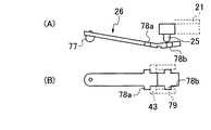
電源供給制御部27は、図2、図3、図6乃至図8に示すように、摺動操作子12の摺動軸21の押込み具合で、モータへの電源を供給する電源スイッチをオン/オフ制御するもので、切替バー26は長尺の導電性板部材で形成され、その一方の端部に電源を供給するための接点77を設け、他方の端部は曲げられ短尺方向に突き出した一対のガイド片78a、78bを備えた構成になっている。
このような切替バー26は、端子片29に備えてある切起こして形成されている切替バー係合部43にガイド片78a、78aの間の板部材を係合させ、後方のガイド片78bを板バネ79で挟持させた状態にして取り付ける。
この切替バー26の接点77は、OFFのときはケース13に配置されている制御素子接続端子片33の電源接点56と対峙した位置関係となっている。
このようにして切替バー26が配置され、その配置された切替バー26の上面に摺動操作子の摺動ノブ25(図3参照)を載せる。摺動ノブ25は、内部にスプリングが組み込まれ、常時付勢した状態に維持することができる。即ち、切替バー26の上面に配置されると、その摺動ノブ25は、切替バー26の上面を付勢した状態となる。そして、摺動操作子12を動作させないときにはスプリングで引き込まれた状態になっているので、摺動ノブ25の位置は、切替バー26のガイド片78bの近傍であり、接点77が上方向に向いた状態、即ち、電源接点56から離れた状態となっている。
As shown in FIGS. 2, 3, and 6 to 8, the power
In such a
When the
Thus, the switching
この状態で摺動操作子12が引き込まれると摺動軸21が動き、図7に示すように、その摺動軸21に連動して動く押圧部材である摺動ノブ25が切替バー26の上面を摺動しながら接点77方向に動く。すると、摺動ノブ25が曲がり部分を通過すると、その曲がりぶんだけ傾斜している上面にのることで、水平方向に戻され、接点77が電源接点56にコンタクトする。これで、図示しない、モータに電源が供給される体制ができ、あとは速度制御部23の制御により、モータの回転速度が制御される。
When the sliding
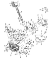
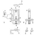
速度制御部23は、図2、図3、図4及び図5に示すように、摺動操作子12に連結され、摺動操作子12に連動する2つの回転制御摺動子22a及びスイッチ摺動子22bを備えた摺動子部64と、ケース13に収納され、第1接触バネ37を係合係止する凸部36を有するプラス電源供給端子片28、第2接触バネ47を係合係止する凸部50を有する制御素子接続端子片31、第3接触バネ58を係合係止する凸部57を有する制御素子接続端子片33、第4接触バネ53を係合係止する凸部52を有するマイナス電源供給端子片32のそれぞれの第1〜第4接触バネ37、47、58、53に電気的に接続するための第1〜第4接触バネ接合部66、67、68、69を備え、且つ摺動操作子12に連動する摺動子部64の回転制御摺動子22a及びスイッチ摺動子22bに弾性接触するための接触子71、72、73、74、75a、75bを備えた摺動回路基板76と、から大略構成されている。
As shown in FIGS. 2, 3, 4, and 5, the
ここで、プラス電源供給端子片28、制御素子接続端子片31、マイナス電源供給端子片32、制御素子接続端子片33については、上述したのでその構造的なものは省略し、又、ケース内部での配置関係も説明したのでその説明も省略する。
Here, since the positive power
摺動回路基板76は、表面に回路素子を搭載し、裏面に第1〜第4接触バネ接合部66、67、68、69、摺動子部64と摺動する接触子71、72、73、74、75a、75bを備えた構造になっており、この基板76は、蓋であるカバーの内側側壁面に係合係止されており、ケース13にカバー17を取付けるときにケース13側の第1〜第4接触バネ37、47、58、53に第1〜第4接触バネ接合部66、67、68、69が当接された状態になり、且つ摺動接点71、72、73、74、75a、75bが摺動子22a、22bに弾性力を付与された状態で当接する。
摺動回路基板76に配設されている接触子は、図14に示すように、平行に且つ整列状態で配設され、上部位置に細長い導電性部材で形成された摺動接触子71、この摺動接触子71の延長線上に設けた抵抗体を構成する可変接触子72、摺動接触子71と平行に隣接した位置に配置した制御接触子73、この制御接触子73の延長線上であって、制御接触子の幅の略半分程度で且つ長さも略半分程度に形成した第1接触子75a、第1接触子75aと一定の間隔を持って同一延長線上に設けた第2接触子75b、第1接触子75a及び第2接触子75bに平行に配置し、略同じ幅であって、第1及び第2接触子75a、75bよりも若干長く形成した補助接触子74からなる。
このように配設された接触子に対して、摺動接触子71及び可変接触子72に対して跨ぐように回転制御摺動子22aが当接されることで可変接触子72の抵抗体を変化させることでモータへの回転制御を行う。
同時に、制御接触子73及び第1接触子75a、第2接触子75b、補助接触子74に対して跨ぐようにスイッチ摺動子22bが当接されることで、制御スイッチとして、並びに補助スイッチとして機能する。
制御スイッチは、制御接触子73と、第1及び第2接触子75a、75bとをスイッチ摺動子22bが導通状態にすることで機能し、補助スイッチは制御接触子73と補助接触子74とをスイッチ摺動子22bが導通状態にすることで機能する。この点については詳細に後述する。
The sliding
As shown in FIG. 14, the contacts arranged on the sliding
The
At the same time, the
The control switch functions by setting the
摺動子部64は、図4に示すように、2個の回転制御摺動子22a及びスイッチ摺動子22bを平行に並べて配置されており、この回転制御摺動子22a及びスイッチ摺動子22bは導電性部材であって細長い板状部材で形成され、全体として弓状になるように形成された両側端部を二股形状に形成し、その二股形状に形成した先端部を上方向折り曲げて更に下方向に折り曲げて接点となし、中央位置に穴を開けて基部から突出したボスに係合した構造となっている。更に、この中央位置に設けた穴の両側端部を直角に折り曲げてへたりを防止した構造となっている。
As shown in FIG. 4, the
このような構造をした摺動子部64は、摺動操作子12が復帰バネ15(図2参照)に抗して操作部11で操作されると回転制御摺動子22a及びスイッチ摺動子22bが摺動回路基板76の接触子71、72、73、74、75a、75bに接触し、この接触状態は、電源供給制御部27の電源スイッチのオン状態等に関連してモータに対して、回転率0パーセントから100パーセントまで制御し、モータ回転率100パーセントにおいてはモータブレーキ及び制御素子短絡部24が動作して短絡状態に制御することで、モータに100パーセントの電源が供給される。
When the sliding
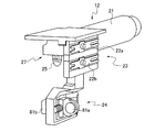
モータブレーキ及び制御素子短絡部24は、図2、図3、図4、図9乃至図11に示すように、略四角形状に繰り抜いた可動枠78にやはり四角形状に形成された摺動枠79が取り付けられ、その内部に2つの短絡接点81a、81bを備えた可動接片82を接点支持バネ83で保持した状態で取り付けられ、可動枠78がこの接点支持バネ83の反対方向から摺動枠79の内壁面に摺動枠バネ84が取り付けられた構成になっている。
摺動枠79には、可動枠78の内周壁面の一部に設けた摺動枠ガイド溝86に係合して動く係止爪87を設け、接点支持バネ83で一方向に当接されている可動接片82が短絡接点81a、81bに印加される押圧に抗して動くことができる可動接片ガイド溝88を設けた構造となっている。
As shown in FIGS. 2, 3, 4, and 9 to 11, the motor brake and control element short-
The sliding
このような構造からなるモータブレーキ及び制御素子短絡部24において、先ず、図9に示す状態において、摺動操作子12が押されると、連結してあるモータブレーキ及び制御素子短絡部24の可動枠78も同じ方向に動き、可動接片82の短絡接点81a、81bがマイナス電源供給端子片32方向に動く。そして図10に示すように、更に摺動操作子12が押されると、可動接片82の短絡接点81aとマイナス電源供給端子片32の接点49、短絡接点81bと端子片29の短絡接点44とが接触する。この状態で更に摺動操作子12が押されると、可動接片82は摺動枠79内において接点支持バネ83の付勢力に抗して可動接片82のみがその位置に留まり摺動枠79自体が摺動操作子12が押される方向に動き、図10に示す位置関係になる。即ち、接点(81aと49、81bと44)同士が接触した状態で、接点支持バネ83により付勢力が加わった状態で接点の接触が維持されるため、その接点状態は極めて良好な関係になる。
In the motor brake and control element short-
次に、摺動操作子12が復帰バネ15によって初期位置に引かれたときには、図11に示すように、可動枠78が連動して動き、摺動枠79の可動接片82の短絡接点81a、81bがプラス電源供給端子片28方向に動くことで、プラス電源供給端子片28のモータブレーキ用接点38に可動接片82の接点81aが接触し、端子片29のモータブレーキ用接点46に可動接片82の接点81bが接触する。そして、接点(38と81a、46と81b)同士が接触した状態で、更に可動枠78が動くと、摺動枠バネ84を押すことで摺動枠79自体が摺動枠ガイド溝86に係合している係止爪87にガイドされて動き、接点同士の接触を摺動枠バネ84の付勢力が加わった状態で保持される。
これらの動作から解かるように、可動接片82に設けられた接点81a、81bは制御素子を短絡してモータを100%回転させる機能と、モータ間を短絡してモータにブレーキをかけるブレーキ機能を有しており、接点のバウンシングが少ない共絡機構を有しながらショート接点、ブレーキ接点を有する機能を有し、部品を減らせる構造となる。
Next, when the sliding
As can be understood from these operations, the
上記説明したスイッチ機構について、図12に示す等価回路を参照して説明すると、モータブレーキ用のモータブレーキ用接点46、38を設け、短絡接点81a、81bを取付けた可動接片82を可動枠78内にスプリング83、84と共に可動するように収納し、操作部11に取付けられた摺動操作子12に取付けられた復帰バネ15と摺動枠バネ84の荷重により可動接片82に取付けた短絡接点81a、81bをモータブレーキ用接点46、38に共絡接触させることで、モータM間は短絡されブレーキがかかった状態になる。
又、操作部11を押し込むと操作部11に連接された摺動操作子12も可動し、ある程度の操作量に達すると可動接片82に取付けた短絡接点81a、81bが制御素子(FET)14のドレインとソースを短絡するための端子片29の短絡接点44とマイナス電源供給端子片32の接点49を共絡接触させ、電源電圧を100%モータに印加させることができる。このとき可動枠78内の接点支持バネ83の荷重により接点接触圧力をある一定以上確保させることができる。
The switch mechanism described above will be described with reference to the equivalent circuit shown in FIG. 12. The
When the
以上のように、摺動操作子12が押されたときでも、引かれたときでも、一対の接点81a、81aはスプリングの付勢力が印加された状態で接触状態を維持するため、少しの振動が加えられてもその接触状態は維持される。
As described above, even when the sliding
さて、以上説明したような構造をしたスイッチ機構を備えたトリガースイッチにおけるトリガースイッチ回路は、摺動回路基板76に設けてある制御スイッチ及び補助スイッチにより制御され、モータへの電源供給を可能にする電源用スイッチ、及び短絡用スイッチを制御することで、モータの回転制御をする。
そのトリガースイッチ回路は、上述したスイッチ機構を構成するもので、操作部11の操作により、モータへの電源の供給を可能にすること、操作部11の操作具合に応じてモータの速度を制御すること、操作部11の操作具合によりモータへの電源を短絡して供給すること、及びモータ停止時にモータを短絡させること、の4つの機能を一つの摺動操作で行うことができる構成になっている。
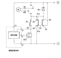
このような機能を有する本発明に係るトリガースイッチ回路は、図13に示すように、摺動回路基板76と、スイッチング素子FETと、モータMと、還流用ダイオードDと、短絡用スイッチSW2と、電源用スイッチSW1と、モータブレーキ用スイッチSW5と、電源Eと、発光手段を構成する発光ダイオードLEDと、抵抗Rとから構成され、これらは次に示すように接続されている。
Now, the trigger switch circuit in the trigger switch having the switch mechanism having the structure as described above is controlled by the control switch and the auxiliary switch provided on the sliding
The trigger switch circuit constitutes the above-described switch mechanism, and enables operation of the
As shown in FIG. 13, the trigger switch circuit according to the present invention having such a function includes a sliding
摺動回路基板76の端子V+と端子V−との間に直列にモータM、電源用スイッチSW1、スイッチング素子FETを接続し、これらと並列に直列接続のダイオードD及び短絡用スイッチSW2を接続し、やはり直列接続のモータM、電源用スイッチSW1、スイッチング素子FETに並列に電源E及びモータブレーキ用スイッチSW5を接続した構成になっている。端子V+と端子V−の間には直列接続の発光ダイオードLED、抵抗Rを備えた構成になっている。
摺動回路基板76内部においては、電源Eを供給する端子V+に補助スイッチSW4が接続され、その出力側に制御スイッチSW3を接続し、抵抗R3を介して端子Gに接続され、スイッチング素子FETのゲートに接続されている。
電源スイッチSW1は、図6乃至図8を参照して説明したように、電源供給制御部27の切替バー26の面上を摺動操作子12の摺動ノブ25が摺動することで、オン/オフするスイッチである。
短絡用スイッチSW2は、図9乃至図11を参照して説明したように、モータブレーキ及び制御素子短絡部24の可動枠78に備えた可動接片82に備えた2つの短絡接点81a、81bが共絡接触するスイッチである。
制御スイッチSW3は、上述した図4及び図5、図14に示すように、第1及び第2接触子75a、75bと制御接触子73の間に跨ぐようにして動くスイッチ摺動子22bの動き具合によりオン/オフするスイッチであり、最初は抵抗R2を介したスイッチをオンにしてスイッチング素子をオンにし、モータが高速回転になると、短絡した状態にオンして電源電圧をスイッチング素子FETのゲートに供給する。
補助スイッチSW4は、上述した図4及び図5、図14に示すように、補助接触子74と制御接触子73の間に跨ぐようにして動くスイッチ摺動子22bの動き具合によりオン/オフするスイッチであり、電源を摺動回路基板に供給するように制御する。
モータブレーキ用スイッチSW5は、モータブレーキ及び制御素子短絡部24の可動枠78に備えた可動片82に備えた2つの短絡接点81a、81bがモータブレーキ用接点46、38に共絡接触したときにオンするスイッチである。即ち、操作部11に取付けられた摺動操作子12に取付けられた復帰バネ15と摺動枠バネ84の荷重により可動接片82に取付けた短絡接点81a、81bをモータブレーキ用接点46、38に共絡接触させることでモータM間は短絡されブレーキがかかった状態になる。
A motor M, a power switch SW1, and a switching element FET are connected in series between the terminal V + and the terminal V- of the sliding
Inside the sliding
As described with reference to FIGS. 6 to 8, the power switch SW <b> 1 is turned on when the sliding
As described with reference to FIGS. 9 to 11, the short-circuit switch SW2 includes two short-
As shown in FIGS. 4, 5, and 14, the control switch SW <b> 3 moves the
As shown in FIGS. 4, 5, and 14, the auxiliary switch SW <b> 4 is turned on / off depending on the movement of the
The motor brake switch SW5 is used when the two short-
このような構成からなるスイッチの動作について、以下説明する。
(1)先ず、図14及び図18に示すように、スイッチ摺動子22bは、制御接触子73を跨いだ状態で位置しているため図13に示す回路のように補助スイッチSW4は開の状態を維持する。このとき操作部11は引かれていないためモータブレーキ用スイッチSW5はオンしており、モータMはブレーキがかかっている。
(2)この状態でトリガー(操作部11)が引かれると、モータブレーキ用スイッチSW5がオフになり、図15及び図18に示すように、連動してスイッチ摺動子22bが動き、第1接触子75aよりも長く設定されている補助接触子74と制御接触子73とを電気的に接続をして補助スイッチSW4がオンになる。補助スイッチSW4がオンになると、図13に示すように、電源Eが発光手段である発光ダイオードLEDに供給され、発光ダイオードLEDが発光する。このとき第1接触子75aとは接触していないため制御スイッチSW3はオフのままである。更に、トリガーが引き込まれると、図6に示す電源用スイッチSW1をオンにする。
(3)更に、トリガーが引かれると、図16及び図18に示すように、スイッチ摺動子22bが連動して動き、制御接触子73と第1接触子75aとを電気的に接続させることで制御スイッチSW3を端子A側に接続してオンにする。制御スイッチSW3がオンすると、図13に示す回路において、電源Eからの電圧が補助スイッチSW4を通り、制御スイッチSW3の第1接触子75aを経由して抵抗R2を介して、スイッチング素子FETのゲートに入力されスイッチング素子FETをオンさせる。
そして、更にトリガーを引き込むことにより、連動する回転制御摺動子22aが引き込まれモータMの回転を制御する。この点については、モータMの回転制御を司る図19に示す回路を参照して後述する。
(4)更に、トリガーが引き込まれると、図17及び図18に示すように、モータMが最高速度回転に制御されると、トリガーの引き込みに連動して動くスイッチ摺動子22bが制御接触子73と第2接触子75bと電気的に接続して制御スイッチSW3を短絡させ(図13で端子Bに接続)スイッチング素子FETのゲートには電源電圧が供給され100%の導通状態になる。この状態で、更にトリガーが引き込まれると、図9及び図10に示す、短絡用スイッチSW2がオンになりモータMを高速に回転制御する。
The operation of the switch having such a configuration will be described below.
(1) First, as shown in FIGS. 14 and 18, since the
(2) When the trigger (operation unit 11) is pulled in this state, the motor brake switch SW5 is turned off, and as shown in FIGS. The
(3) Further, when the trigger is pulled, as shown in FIGS. 16 and 18, the
Then, by further pulling the trigger, the interlocking
(4) Further, when the trigger is pulled, as shown in FIGS. 17 and 18, when the motor M is controlled to rotate at the maximum speed, the
このようにして、電源用スイッチSW1がオンになるときには、スイッチング素子FETのゲートに供給する電圧を制御スイッチSW3がオフのため、遮断状態での電源用スイッチSW1をオンにできるため、電源用スイッチSW1には電位差がない状態でオンできる。
更に、短絡用スイッチSW2をオンにするときには、スイッチング素子FETのゲートには電源電圧が供給されて100%導通状態で、短絡用スイッチSW2がオンできるため、やはり電位差のない状態でオンすることができるのである。
Thus, when the power switch SW1 is turned on, the voltage supplied to the gate of the switching element FET can be turned on because the control switch SW3 is turned off, so that the power switch SW1 in the cut-off state can be turned on. SW1 can be turned on with no potential difference.
Further, when the shorting switch SW2 is turned on, since the power supply voltage is supplied to the gate of the switching element FET and the shorting switch SW2 can be turned on in a 100% conduction state, it can be turned on without any potential difference. It can be done.
図19は、トリガーの引き込みに連動して動く回転制御摺動子22aに基づくモータの回転制御をするためのスイッチ回路を示したものであり、基準信号を出力する基準信号出力手段である三角波発振回路、操作レバーの操作具合に基づいて所定の操作信号を出力する操作信号出力手段と、基準信号出力手段からの基準信号を一方の入力端子(プラス側入力端子)に入力し、操作信号出力手段からの操作信号を他方の入力端子(マイナス側入力端子)に入力し、その入力された信号を比較して所定の制御信号を前記スイッチング素子に供給してスイッチング素子FETをオン/オフ制御するコンパレータCOMPと、を備えており、
操作信号出力手段は、電源Eに接続されている端子V+と端子V−との間に直列接続した抵抗R5(Ra)、抵抗R6(Rc)、抵抗R7(Re)を備え、抵抗R6(Rc)に並列に可変接触子72を配設し、可変接触子72と摺動接触子71に跨ぐように回転制御摺動子22aを備えた構成になっており、摺動接触子71に接続した抵抗R12(Rd)を介してコンパレータCOMPのマイナス側入力端子に接続されている。このマイナス側入力端子にはスイッチSW6を介して抵抗R5と抵抗R6の中間に接続されている。
コンパレータCOMPのプラス側入力端子は三角波発振回路の三角波信号(基準信号)を入力する。コンパレータCOMPの出力端子は端子Gに接続され、スイッチング素子FETのゲートに接続され、制御信号をスイッチング素子FETに供給する。
回転制御摺動子22aは、上述した図4及び図5、図14に示すように、速度制御部23においてモータの回転制御を司るもので、スイッチ摺動子22bと一緒に連動するものであり、摺動接触子71と可変接触子72に跨ぐようにして配置され、摺動操作子の引き具合により、可変抵触子72上を摺動することで、抵抗値が変化することでモータの回転を制御する。
スイッチSW6は、モータが高速回転するときに機能するスイッチであり、低速回転時には可変接触子72が短絡した状態になるため、スイッチをオンしてもオフしても回転動作に影響を与えない。これについては、後述する等価回路の図22を用いて計算される出力電圧V'が可変であることにより証明される。
FIG. 19 shows a switch circuit for controlling the rotation of the motor based on the
The operation signal output means includes a resistor R5 (Ra), a resistor R6 (Rc), and a resistor R7 (Re) connected in series between a terminal V + and a terminal V− connected to the power source E, and a resistor R6 (Rc The
The positive side input terminal of the comparator COMP inputs the triangular wave signal (reference signal) of the triangular wave oscillation circuit. The output terminal of the comparator COMP is connected to the terminal G, is connected to the gate of the switching element FET, and supplies a control signal to the switching element FET.
As shown in FIGS. 4, 5, and 14 described above, the
The switch SW6 is a switch that functions when the motor rotates at a high speed. Since the
図21は、回転制御摺動子22a、摺動接触子71、可変接触子72で構成される回路の等価回路であり、電源Vと接地間に直列に抵抗Ra、可変接触子72である可変抵抗Rc、抵抗Reを接続し、可変抵抗Rcに並列に抵抗Rbを接続し、可変接触子72と摺動接触子71を跨いで電気的に接続する回転制御摺動子22aを備え、可変接触子72の開始位置と抵抗Rdの出力側の間に高速回転用のスイッチSW6を備えた構成になっている。
FIG. 21 is an equivalent circuit of a circuit composed of the
このような構成からなるスイッチ回路において、回転制御摺動子22aが可変接触子72の開始位置(図21で丸Aの位置)の場合には、図22に示すように、所謂、モータが低速回転のときであり、スイッチSW6がオン/オフのいずれの場合も、回転制御摺動子22aは短絡した状態となり、出力電圧V'は、次式で示すことができる。
V'
=Rb・Rc/(Rb+Rc)+Re/
Ra+Re+Rb・Rc/Rb+Rc・V
=(((Rb・Rc+Rb・Re+Rc・Re)/(Rb+Rc))/
((Ra・Rb+Rb・Re+Ra・Rc+Rc・Re+Rb・Rc)/(Rb+Rc)))・V
=((Rb・Rc+Rb・Re+Rc・Re)/
(Ra・Rb+Rb・Re+Ra・Rc+Rc・Re+Rb・Rc))・V
In the switch circuit having such a configuration, when the
V '
= Rb · Rc / (Rb + Rc) + Re /
Ra + Re + Rb.Rc / Rb + Rc.V
= (((Rb · Rc + Rb · Re + Rc · Re) / (Rb + Rc)) /
((Ra · Rb + Rb · Re + Ra · Rc + Rc · Re + Rb · Rc) / (Rb + Rc))) · V
= ((Rb · Rc + Rb · Re + Rc · Re) /
(Ra * Rb + Rb * Re + Ra * Rc + Rc * Re + Rb * Rc)) * V
回転制御摺動子が可変接触子の終了位置(図21で丸Bの位置)の場合には、図23に示すように、所謂、モータが高速回転のときであり、スイッチSW6のオン/オフにより出力する電圧に変化がある。スイッチSW6がオンのときの出力電圧V'は、次式で示すことができる。
V'
=((((Rb・Rc・Rd)/(Rb・Rc+Rb・Rd+Rb・Rc))+Re)/
(Ra+Re+(Rb・Rc・Rd)/(Rb・Rc+Rb・Rd+Rc・Rd)))・V
=(((Ra・Rc・Rd+Rb・Rc・Re+Rb・Rd・Re+Rb・Rc・Re)/(Rb・Rc+Rb・Rd+Rb・Rc))/
(Ra・Rb・Rc+Ra・Rb・Rd+Ra・Rc・Rd+Rb・Rc・Re+Rb・Rd・Re+Rc・Rd・Re+Rb・Rc・Rd)/(Rb・Rc+Rb・Rd+Rc・Rd))・V
=((Ra・Rc・Rd+Rb・Rc・Re+Rb・Rd・Re+Rb・Rc・Re)/
(Ra・Rb・Rc+Ra・Rb・Rd+Ra・Rc・Rd+Rb・Rc・Re+Rb・Rd・Re+Rc・Rd・Re+Rb・Rc・Rd))・V
When the rotation control slider is at the end position of the variable contact (the position of circle B in FIG. 21), as shown in FIG. 23, this is a so-called motor rotation, and the switch SW6 is turned on / off. There is a change in the output voltage. The output voltage V ′ when the switch SW6 is on can be expressed by the following equation.
V '
= (((((Rb.Rc.Rd) / (Rb.Rc + Rb.Rd + Rb.Rc)) + Re) /
(Ra + Re + (Rb * Rc * Rd) / (Rb * Rc + Rb * Rd + Rc * Rd))) * V
= (((Ra * Rc * Rd + Rb * Rc * Re + Rb * Rd * Re + Rb * Rc * Re) / (Rb * Rc + Rb * Rd + Rb * Rc)) /
(Ra * Rb * Rc + Ra * Rb * Rd + Ra * Rc * Rd + Rb * Rc * Re + Rb * Rd * Re + Rc * Rd * Re + Rb * Rc * Rd) / (Rb * Rc + Rb * Rd + Rc * Rd)) * V
= ((Ra · Rc · Rd + Rb · Rc · Re + Rb · Rd · Re + Rb · Rc · Re) /
(Ra.Rb.Rc + Ra.Rb.Rd + Ra.Rc.Rd + Rb.Rc.Re + Rb.Rd.Re + Rc.Rd.Re + Rb.Rc.Rd)). V
スイッチSW6がオフの時の出力電圧V'は、次式で示すことができ、オンのときよりも高速に回転させることができる。
V'
=(Re/
(Ra+Re+(Rb・Rc/(Rb+Rc)))・V
=(Re/
(Ra・Rb+Ra・Rc+Rb・Re+Rc・Re+Rb・Rc)/(Rb+Rc))・V
=((Re・(Rb+Rc))/
(Ra・Rb+Ra・Rc+Rb・Re+Rc・Re+Rb・Rc))・V
The output voltage V ′ when the switch SW6 is off can be expressed by the following equation and can be rotated at a higher speed than when it is on.
V '
= (Re /
(Ra + Re + (Rb.Rc / (Rb + Rc))). V
= (Re /
(Ra * Rb + Ra * Rc + Rb * Re + Rc * Re + Rb * Rc) / (Rb + Rc)) * V
= ((Re · (Rb + Rc)) /
(Ra * Rb + Ra * Rc + Rb * Re + Rc * Re + Rb * Rc)) * V
このようにして、モータ回転数はコンパレータのマイナス側入力端子へ入力される可変接触子72と抵抗で分電圧された電圧とプラス側入力端子へ入力される三角波信号を比較して制御する。スイッチSW6は、図20に示すように、1個のスイッチにして低速回転数一定で高速回転を可変することが実現できるのである。
このように、1個のスイッチSW6のオン/オフだけで高速回転数を設定することができるため電動工具への取付け性が向上するとともにスイッチ1個分のコストダウンも可能になる。又、摺動回路基板の配線も簡略化できるためスイッチ組立て工数の削減も可能である。
In this way, the motor speed is controlled by comparing the
As described above, since the high-speed rotation speed can be set only by turning on / off one switch SW6, the attachment to the electric tool is improved and the cost for one switch can be reduced. Also, since the wiring of the sliding circuit board can be simplified, the number of switch assembly steps can be reduced.
スイッチング素子を遮断状態のときに電源用スイッチをオンし、スイッチング素子が100%導通した状態のときに短絡用スイッチをオンするようにしたため、いわば電位差をなくした状態でスイッチをオンするようにしたことで、両スイッチの接点間に発生するスパークを極めて少なくすることができ、接点の寿命を延ばすことができるトリガースイッチ回路を提供する。
又、モータが回転する前にLEDを点灯できるようにしたことで、電動工具に使用した場合、モータが回転する前にLEDがオンし、被切削物に照射させることが出来るため、位置決め等の使い勝手がよいトリガースイッチ回路を提供する。
更に、1個のスイッチSW6のオン/オフだけで高速回転数を設定することができるため電動工具への取付け性が向上するとともにスイッチ1個分のコストダウンも可能になり、又、摺動回路基板の配線も簡略化できるためスイッチ組立て工数の削減も可能なトリガースイッチ回路を提供する。
The power switch is turned on when the switching element is cut off, and the shorting switch is turned on when the switching element is 100% conductive, so the switch is turned on with the potential difference eliminated. Thus, it is possible to provide a trigger switch circuit capable of extremely reducing the spark generated between the contacts of both switches and extending the life of the contacts.
In addition, since the LED can be lit before the motor rotates, when used in an electric tool, the LED can be turned on before the motor rotates to irradiate the workpiece. Provide a trigger switch circuit that is easy to use.
Furthermore, since the high-speed rotation speed can be set only by turning on / off one switch SW6, the attachment to the electric tool is improved and the cost for one switch can be reduced. Provided is a trigger switch circuit capable of simplifying wiring of a substrate and reducing the number of switch assembly steps.
11;操作部、12;摺動操作子、13;ケース、14;制御素子(FET)、16;FET配置部、17;カバー、18;切替操作部、19;放熱板、21;摺動軸、22a;回転制御摺動子、22b;スイッチ摺動子、23;速度制御部、24;モータブレーキ短絡部、25;摺動ノブ、26;切替バー、27;電源供給制御部、28;プラス電源供給端子片、29;端子片、31;制御素子接続端子片、32;マイナス電源供給端子片、33;制御素子接続端子片、36;凸部、37;第1接触バネ、38;モータブレーキ用接点、39;ダイオード、41;ダイオード接続部、41a;ダイオード接続部、41b;ダイオード接続部、42;接続部、44;短絡接点、46;モータブレーキ用接点、47;第2接触バネ、48;接続部、49;接点、50;凸部、51;中間接続部、52;凸部、53;第4接触バネ、54;接続部、56;電源接点、57;凸部、58;第3接触バネ、59;接続部、61a;同軸係合穴、61b;同軸係合穴、62a;パッキン、62b;パッキン、63a;パッキン収納部、63b;パッキン収納部、64;摺動子部、66;第1接触バネ接合部、67;第2接触バネ接合部、68;第3接触バネ接合部、69;第4接触バネ接合部、71;摺動接触子、72;可変接触子、73;制御接触子、74;補助接触子、75a;第1接触子、75b:第2接触子、76;摺動回路基板、77;接点、78;可動枠、78a;ガイド片、78b;ガイド片、79;摺動枠、81a;短絡接点、81b;短絡接点、82;可動接片、83;接点支持バネ、84;摺動枠バネ、86;摺動枠ガイド溝、87;係止爪、88;可動接片ガイド溝。 DESCRIPTION OF SYMBOLS 11; Operation part, 12; Sliding operation element, 13; Case, 14; Control element (FET), 16; FET arrangement | positioning part, 17; Cover, 18; Switching operation part, 19; , 22a; rotation control slider, 22b; switch slider, 23; speed control section, 24; motor brake short-circuit section, 25; sliding knob, 26; switching bar, 27; power supply control section, 28; Power supply terminal piece 29, terminal piece 31, control element connection terminal piece 32, negative power supply terminal piece 33, control element connection terminal piece 36, convex part 37, first contact spring 38, motor brake Contact point 39; diode 41; diode connection part 41a; diode connection part 41b; diode connection part 42; connection part 44; short-circuit contact 46; motor brake contact 47; second contact spring 48 Connection , 49; contact, 50; convex, 51; intermediate connection, 52; convex, 53; fourth contact spring, 54; connection, 56; power contact, 57; convex, 58; 59; connection portion, 61a; coaxial engagement hole, 61b; coaxial engagement hole, 62a; packing, 62b; packing, 63a; packing storage portion, 63b; packing storage portion, 64; slider portion, 66; Contact spring joint, 67; second contact spring joint, 68; third contact spring joint, 69; fourth contact spring joint, 71; sliding contact, 72; variable contact, 73; 74; auxiliary contact, 75a; first contact, 75b: second contact, 76; sliding circuit board, 77; contact, 78; movable frame, 78a; guide piece, 78b; guide piece, 79; Moving frame, 81a; short circuit contact, 81b; short circuit contact, 82; movable contact, 83; contact Support springs, 84; slide frame spring, 86; slide frame guide groove, 87; locking pawl, 88; movable contact piece guide groove.
Claims (4)
前記電源用スイッチと、前記短絡用スイッチと、前記モータブレーキスイッチと、前記制御スイッチと、前記補助スイッチの五者を前記トリガーと連動して動作する構成にし、
前記トリガーが引き込まれたときに、前記補助スイッチをオンにして前記駆動部に電源を供給し、
更に、トリガーが引き込まれたときに、前記電源用スイッチをオンに制御して前記モータに電源を供給し、
更に、トリガーが引き込まれたときに、前記制御スイッチをオンに制御して抵抗を介した電圧を前記スイッチング素子のゲートに供給するように制御し、
更に、トリガーが引き込まれたときに、前記制御スイッチのオン状態を直流電源を直接供給する位置にして、前記スイッチング素子のゲートに直流電源を直接供給することで、前記スイッチング素子を100%導通できる状態にし、
更に、トリガーを引き込むことで、前記短絡スイッチをオンに制御するようにしたことを特徴とするトリガースイッチ回路。 A power switch provided between the DC power supply and the motor, a switching element connected in series with the motor, a short-circuit switch connected in parallel to the switching element, a motor brake switch for stopping the motor, and the switching element A trigger comprising: a drive unit to be driven; a control switch that supplies a voltage to the gate of the switching element when the trigger is pulled; and an auxiliary switch that supplies a DC power source to the drive unit when the trigger is pulled A switch circuit,
The power switch, the shorting switch, the motor brake switch, the control switch, and the auxiliary switch are configured to operate in conjunction with the trigger,
When the trigger is pulled in, turn on the auxiliary switch to supply power to the drive unit,
Furthermore, when the trigger is pulled, the power switch is turned on to supply power to the motor,
Further, when the trigger is pulled, the control switch is turned on to control the voltage via the resistor to be supplied to the gate of the switching element,
Further, when the trigger is pulled in, the switching element can be made 100% conductive by setting the ON state of the control switch to a position for directly supplying DC power and supplying DC power directly to the gate of the switching element. State
Further, the trigger switch circuit is characterized in that the short-circuit switch is controlled to be turned on by pulling in the trigger.
操作レバーの操作具合に基づいて所定の操作信号を出力する操作信号出力手段と、
モータと直列に接続され、モータの回転制御をするスイッチング素子と、
前記基準信号出力手段からの基準信号を一方の入力端子に入力し、前記操作信号出力手段からの操作信号を他方の入力端子に入力し、その入力された信号を比較して所定の制御信号を前記スイッチング素子に供給してスイッチング素子をオン/オフ制御するコンパレータと、を備えたトリガースイッチ回路であって、
前記操作信号出力手段は、電源と接地間に直列に抵抗Ra、可変抵抗Rc、抵抗Reを接続し、前記可変抵抗Rcに並列に抵抗Rbを接続し、可変接触子72と摺動接触子71を跨いで電気的に接続する回転制御摺動子22aを備え、前記可変接触子72の開始位置と回転制御摺動子22aに接続されている抵抗Rdの出力側の間に高速回転用のスイッチSW6を備えたことを特徴とするトリガースイッチ回路。 A reference signal output means for outputting a reference signal;
Operation signal output means for outputting a predetermined operation signal based on the operating condition of the operation lever;
A switching element connected in series with the motor and controlling the rotation of the motor;
A reference signal from the reference signal output means is input to one input terminal, an operation signal from the operation signal output means is input to the other input terminal, and the input signal is compared to obtain a predetermined control signal. A comparator that supplies the switching element to control on / off of the switching element, and a trigger switch circuit comprising:
The operation signal output means connects a resistor Ra, a variable resistor Rc, and a resistor Re in series between a power source and the ground, and connects a resistor Rb in parallel to the variable resistor Rc. A variable contact 72 and a sliding contact 71 A switch for high-speed rotation between the starting position of the variable contact 72 and the output side of the resistor Rd connected to the rotation control slider 22a. A trigger switch circuit comprising SW6.
Priority Applications (5)
| Application Number | Priority Date | Filing Date | Title |
|---|---|---|---|
| JP2005032943A JP4354921B2 (en) | 2005-02-09 | 2005-02-09 | Trigger switch circuit, electric tool and trigger switch |
| DE602006014036T DE602006014036D1 (en) | 2005-02-09 | 2006-02-07 | trigger switch |
| EP06002451A EP1691385B1 (en) | 2005-02-09 | 2006-02-07 | Trigger switch |
| US11/349,112 US7511240B2 (en) | 2005-02-09 | 2006-02-08 | Trigger switch |
| CN 200610004579 CN1819085B (en) | 2005-02-09 | 2006-02-09 | Trigger switch |
Applications Claiming Priority (1)
| Application Number | Priority Date | Filing Date | Title |
|---|---|---|---|
| JP2005032943A JP4354921B2 (en) | 2005-02-09 | 2005-02-09 | Trigger switch circuit, electric tool and trigger switch |
Publications (3)
| Publication Number | Publication Date |
|---|---|
| JP2006221908A true JP2006221908A (en) | 2006-08-24 |
| JP2006221908A5 JP2006221908A5 (en) | 2009-03-26 |
| JP4354921B2 JP4354921B2 (en) | 2009-10-28 |
Family
ID=36984084
Family Applications (1)
| Application Number | Title | Priority Date | Filing Date |
|---|---|---|---|
| JP2005032943A Expired - Fee Related JP4354921B2 (en) | 2005-02-09 | 2005-02-09 | Trigger switch circuit, electric tool and trigger switch |
Country Status (1)
| Country | Link |
|---|---|
| JP (1) | JP4354921B2 (en) |
Cited By (12)
| Publication number | Priority date | Publication date | Assignee | Title |
|---|---|---|---|---|
| JP2008243698A (en) * | 2007-03-28 | 2008-10-09 | Omron Corp | Trigger switch |
| JP2008296323A (en) * | 2007-05-31 | 2008-12-11 | Hitachi Koki Co Ltd | Power tool |
| JP2009135000A (en) * | 2007-11-30 | 2009-06-18 | Satori S-Tech Co Ltd | Trigger switch |
| JP2010027385A (en) * | 2008-07-18 | 2010-02-04 | Satori S-Tech Co Ltd | Trigger switch circuit |
| JP2012094553A (en) * | 2012-02-17 | 2012-05-17 | Satori S-Tech Co Ltd | Trigger switch |
| JP2012157942A (en) * | 2011-02-01 | 2012-08-23 | Hitachi Koki Co Ltd | Electric power tool |
| EP2530694A1 (en) | 2011-05-31 | 2012-12-05 | Omron Corporation | Trigger switch circuit and electric instrument |
| US8446120B2 (en) | 2011-05-19 | 2013-05-21 | Black & Decker Inc. | Electronic switching module for a power tool |
| EP2709133A1 (en) | 2012-09-13 | 2014-03-19 | Panasonic Corporation | Trigger switch and power tool |
| WO2018123223A1 (en) * | 2016-12-28 | 2018-07-05 | オムロン株式会社 | Contact structure for switch, trigger switch and electric power tool |
| US10608501B2 (en) | 2017-05-24 | 2020-03-31 | Black & Decker Inc. | Variable-speed input unit having segmented pads for a power tool |
| JP2022120806A (en) * | 2021-02-05 | 2022-08-18 | ディーフォン エレクテック カンパニー リミテッド | snap action switch |
-
2005
- 2005-02-09 JP JP2005032943A patent/JP4354921B2/en not_active Expired - Fee Related
Cited By (21)
| Publication number | Priority date | Publication date | Assignee | Title |
|---|---|---|---|---|
| JP2008243698A (en) * | 2007-03-28 | 2008-10-09 | Omron Corp | Trigger switch |
| JP2008296323A (en) * | 2007-05-31 | 2008-12-11 | Hitachi Koki Co Ltd | Power tool |
| JP2009135000A (en) * | 2007-11-30 | 2009-06-18 | Satori S-Tech Co Ltd | Trigger switch |
| JP2010027385A (en) * | 2008-07-18 | 2010-02-04 | Satori S-Tech Co Ltd | Trigger switch circuit |
| JP2012157942A (en) * | 2011-02-01 | 2012-08-23 | Hitachi Koki Co Ltd | Electric power tool |
| US9000882B2 (en) | 2011-05-19 | 2015-04-07 | Black & Decker Inc. | Electronic switching module for a power tool |
| US10256697B2 (en) | 2011-05-19 | 2019-04-09 | Black & Decker Inc. | Electronic switching module for a power tool |
| US10651706B2 (en) | 2011-05-19 | 2020-05-12 | Black & Decker Inc. | Control unit for a power tool |
| US8446120B2 (en) | 2011-05-19 | 2013-05-21 | Black & Decker Inc. | Electronic switching module for a power tool |
| US9406457B2 (en) | 2011-05-19 | 2016-08-02 | Black & Decker Inc. | Electronic switching module for a power tool |
| US9401250B2 (en) | 2011-05-19 | 2016-07-26 | Black & Decker, Inc. | Electronic switching module for a power tool |
| EP2530694A1 (en) | 2011-05-31 | 2012-12-05 | Omron Corporation | Trigger switch circuit and electric instrument |
| CN102809949A (en) * | 2011-05-31 | 2012-12-05 | 欧姆龙株式会社 | Trigger switch circuit and electric instrument |
| JP2012094553A (en) * | 2012-02-17 | 2012-05-17 | Satori S-Tech Co Ltd | Trigger switch |
| EP2709133A1 (en) | 2012-09-13 | 2014-03-19 | Panasonic Corporation | Trigger switch and power tool |
| WO2018123223A1 (en) * | 2016-12-28 | 2018-07-05 | オムロン株式会社 | Contact structure for switch, trigger switch and electric power tool |
| JP2018107088A (en) * | 2016-12-28 | 2018-07-05 | オムロン株式会社 | Contact structure of switch, trigger switch, and power tool |
| US10770245B2 (en) | 2016-12-28 | 2020-09-08 | Omron Corporation | Contact structure for switch, trigger switch and electric power tool |
| US10608501B2 (en) | 2017-05-24 | 2020-03-31 | Black & Decker Inc. | Variable-speed input unit having segmented pads for a power tool |
| JP2022120806A (en) * | 2021-02-05 | 2022-08-18 | ディーフォン エレクテック カンパニー リミテッド | snap action switch |
| JP7261329B2 (en) | 2021-02-05 | 2023-04-19 | ディーフォン エレクテック カンパニー リミテッド | snap action switch |
Also Published As
| Publication number | Publication date |
|---|---|
| JP4354921B2 (en) | 2009-10-28 |
Similar Documents
| Publication | Publication Date | Title |
|---|---|---|
| JP4354921B2 (en) | Trigger switch circuit, electric tool and trigger switch | |
| US7511240B2 (en) | Trigger switch | |
| JP5033543B2 (en) | Trigger switch | |
| US7638725B2 (en) | Switch for electric power tool | |
| EP1975956B1 (en) | Trigger Switch | |
| CN1819085B (en) | Trigger switch | |
| JP5764388B2 (en) | Trigger switch for electric tools | |
| WO2018123223A1 (en) | Contact structure for switch, trigger switch and electric power tool | |
| JP2006221908A5 (en) | ||
| US20210304975A1 (en) | Trigger switch | |
| KR101489112B1 (en) | Interior lamp for vehicle | |
| JP2007000982A (en) | Volume switch of power tool and power tool provided therewith | |
| JP5226410B2 (en) | Trigger switch circuit | |
| JP5351555B2 (en) | Power tool switch | |
| JP4879608B2 (en) | Electric tool | |
| JP2009218064A (en) | Slide operation type electric component | |
| JP4354293B2 (en) | Electromagnetic relay device | |
| JP3671049B2 (en) | Electric tool | |
| KR200438155Y1 (en) | Electric parking brake switch circuit | |
| JPH0311492B2 (en) | ||
| US9741510B2 (en) | Switch device | |
| JP4455864B2 (en) | Mounting structure of sliding resistance board in power tool switch | |
| JP2012196732A (en) | Switch for electric power tool | |
| JP2697053B2 (en) | Power tool switch | |
| JPH0347223Y2 (en) |
Legal Events
| Date | Code | Title | Description |
|---|---|---|---|
| A621 | Written request for application examination |
Free format text: JAPANESE INTERMEDIATE CODE: A621 Effective date: 20061212 |
|
| A521 | Request for written amendment filed |
Free format text: JAPANESE INTERMEDIATE CODE: A523 Effective date: 20090202 |
|
| A977 | Report on retrieval |
Free format text: JAPANESE INTERMEDIATE CODE: A971007 Effective date: 20090703 |
|
| TRDD | Decision of grant or rejection written | ||
| A01 | Written decision to grant a patent or to grant a registration (utility model) |
Free format text: JAPANESE INTERMEDIATE CODE: A01 Effective date: 20090707 |
|
| A01 | Written decision to grant a patent or to grant a registration (utility model) |
Free format text: JAPANESE INTERMEDIATE CODE: A01 |
|
| A61 | First payment of annual fees (during grant procedure) |
Free format text: JAPANESE INTERMEDIATE CODE: A61 Effective date: 20090730 |
|
| R150 | Certificate of patent or registration of utility model |
Ref document number: 4354921 Country of ref document: JP Free format text: JAPANESE INTERMEDIATE CODE: R150 Free format text: JAPANESE INTERMEDIATE CODE: R150 |
|
| FPAY | Renewal fee payment (event date is renewal date of database) |
Free format text: PAYMENT UNTIL: 20120807 Year of fee payment: 3 |
|
| FPAY | Renewal fee payment (event date is renewal date of database) |
Free format text: PAYMENT UNTIL: 20120807 Year of fee payment: 3 |
|
| FPAY | Renewal fee payment (event date is renewal date of database) |
Free format text: PAYMENT UNTIL: 20130807 Year of fee payment: 4 |
|
| R250 | Receipt of annual fees |
Free format text: JAPANESE INTERMEDIATE CODE: R250 |
|
| R250 | Receipt of annual fees |
Free format text: JAPANESE INTERMEDIATE CODE: R250 |
|
| R250 | Receipt of annual fees |
Free format text: JAPANESE INTERMEDIATE CODE: R250 |
|
| R250 | Receipt of annual fees |
Free format text: JAPANESE INTERMEDIATE CODE: R250 |
|
| R250 | Receipt of annual fees |
Free format text: JAPANESE INTERMEDIATE CODE: R250 |
|
| R250 | Receipt of annual fees |
Free format text: JAPANESE INTERMEDIATE CODE: R250 |
|
| S111 | Request for change of ownership or part of ownership |
Free format text: JAPANESE INTERMEDIATE CODE: R313111 |
|
| R350 | Written notification of registration of transfer |
Free format text: JAPANESE INTERMEDIATE CODE: R350 |
|
| R250 | Receipt of annual fees |
Free format text: JAPANESE INTERMEDIATE CODE: R250 |
|
| R250 | Receipt of annual fees |
Free format text: JAPANESE INTERMEDIATE CODE: R250 |
|
| R250 | Receipt of annual fees |
Free format text: JAPANESE INTERMEDIATE CODE: R250 |
|
| R250 | Receipt of annual fees |
Free format text: JAPANESE INTERMEDIATE CODE: R250 |
|
| LAPS | Cancellation because of no payment of annual fees |