JP2006201416A - Projection type display device and multi-screen display device - Google Patents
Projection type display device and multi-screen display device Download PDFInfo
- Publication number
- JP2006201416A JP2006201416A JP2005012232A JP2005012232A JP2006201416A JP 2006201416 A JP2006201416 A JP 2006201416A JP 2005012232 A JP2005012232 A JP 2005012232A JP 2005012232 A JP2005012232 A JP 2005012232A JP 2006201416 A JP2006201416 A JP 2006201416A
- Authority
- JP
- Japan
- Prior art keywords
- display device
- light
- projection
- detector
- projection lens
- Prior art date
- Legal status (The legal status is an assumption and is not a legal conclusion. Google has not performed a legal analysis and makes no representation as to the accuracy of the status listed.)
- Granted
Links
Images

Classifications
-
- H—ELECTRICITY
- H04—ELECTRIC COMMUNICATION TECHNIQUE
- H04N—PICTORIAL COMMUNICATION, e.g. TELEVISION
- H04N9/00—Details of colour television systems
- H04N9/12—Picture reproducers
- H04N9/31—Projection devices for colour picture display, e.g. using electronic spatial light modulators [ESLM]
- H04N9/3191—Testing thereof
- H04N9/3194—Testing thereof including sensor feedback
-
- H—ELECTRICITY
- H04—ELECTRIC COMMUNICATION TECHNIQUE
- H04N—PICTORIAL COMMUNICATION, e.g. TELEVISION
- H04N9/00—Details of colour television systems
- H04N9/12—Picture reproducers
- H04N9/31—Projection devices for colour picture display, e.g. using electronic spatial light modulators [ESLM]
- H04N9/3141—Constructional details thereof
- H04N9/3147—Multi-projection systems
-
- H—ELECTRICITY
- H04—ELECTRIC COMMUNICATION TECHNIQUE
- H04N—PICTORIAL COMMUNICATION, e.g. TELEVISION
- H04N9/00—Details of colour television systems
- H04N9/12—Picture reproducers
- H04N9/31—Projection devices for colour picture display, e.g. using electronic spatial light modulators [ESLM]
- H04N9/3179—Video signal processing therefor
- H04N9/3182—Colour adjustment, e.g. white balance, shading or gamut
-
- H—ELECTRICITY
- H04—ELECTRIC COMMUNICATION TECHNIQUE
- H04N—PICTORIAL COMMUNICATION, e.g. TELEVISION
- H04N5/00—Details of television systems
- H04N5/44—Receiver circuitry for the reception of television signals according to analogue transmission standards
- H04N5/57—Control of contrast or brightness
- H04N5/58—Control of contrast or brightness in dependence upon ambient light
Landscapes
- Engineering & Computer Science (AREA)
- Multimedia (AREA)
- Signal Processing (AREA)
- Projection Apparatus (AREA)
- Control Of Indicators Other Than Cathode Ray Tubes (AREA)
- Liquid Crystal (AREA)
- Controls And Circuits For Display Device (AREA)
Abstract
【課題】
投射型表示装置において、表示領域内の光強度を投射光の乱反射光を検出することにより把握し、自動的に調整することで光学部品の経時変化を低減し良好な映像を表示する。
【解決手段】
本発明の投射型表示装置は、光源(20)、光源からの光を駆動電圧に応じて変調し光学像を形成する表示デバイス(29,34,42)、表示デバイス上の光学像を拡大投影する投射レンズ(15)、該投射レンズからの光を検出する検出器(5)、及び該検出器の出力に応じて前記駆動電圧を制御する制御回路(11)を有する。そしてこの検出器は、投射レンズから出射される光束の外縁近傍に配置され、投射レンズからの光のうちスクリーン(45)の有効領域外に到達する光(乱反射光)を検出する。
【選択図】 図1【Task】
In the projection type display device, the light intensity in the display area is grasped by detecting irregularly reflected light of the projected light, and automatically adjusted to reduce the temporal change of the optical components and display a good image.
[Solution]
The projection display device of the present invention includes a light source (20), a display device (29, 34, 42) that modulates light from the light source according to a driving voltage to form an optical image, and an optical image on the display device is enlarged and projected A projection lens (15), a detector (5) for detecting light from the projection lens, and a control circuit (11) for controlling the drive voltage in accordance with the output of the detector. The detector is disposed in the vicinity of the outer edge of the light beam emitted from the projection lens, and detects light (diffuse reflected light) reaching the outside of the effective area of the screen (45) among the light from the projection lens.
[Selection] Figure 1
Description
本発明は、液晶などの表示デバイス上に形成した光学像を拡大して投射する投射型表示装置、およびそれを用いたマルチスクリーン表示装置に関する。 The present invention relates to a projection display device that enlarges and projects an optical image formed on a display device such as a liquid crystal, and a multi-screen display device using the same.
従来の投射型表示装置においては、一般に光源にはランプが使用されるが、このランプは使用初期の段階では輝度が高く、使用時間が長くなるにつれて輝度が低下する。この輝度低下を補償する従来技術としては、例えば特許文献1、2に記載のものが知られている。特許文献1には、投射型表示装置のスクリーン近傍に明るさ(輝度)を検出する光検出器(以下、「検出器」と省略する)を配置し、その検出出力に応じて光源に供給する入力パワーの大きさを調整して、スクリーン上での明るさが一定となるように制御する技術が開示されている。また特許文献2には、検出器を光源から表示デバイスに至るまでの光路途中に配置し、特許文献1と同様に、検出器の出力に応じて光源に供給する入力パワーの大きさを調整するようにして、スクリーン上での明るさが一定となるように制御する技術が開示されている。
In a conventional projection display device, a lamp is generally used as a light source, but this lamp has a high luminance at the initial stage of use, and the luminance decreases as the usage time becomes longer. For example,
特許文献1に記載された技術においては、スクリーンの近傍の有効領域内に検出器を配置している。このため、スクリーンの周囲の光(例えば投射型表示装置が設置されている部屋の照明光)の影響により投射レンズからの輝度を正しく測定できない可能性がある。さらにスクリーン近傍の有効領域内に検出器を配置しているため、検出器の影が映像に影響してしまい、常時配置して調整することができない。
In the technique described in
特許文献2においては、光源から表示デバイスに至るまでの密閉構造の光路途中に検出器を配置しているため、特許文献1のように周囲光の影響は受けない。しかしながら、経時変化するのは光源だけではなく、偏光板や表示デバイスなどの光学部品が光源からの光に含まれる紫外線により劣化され得る。したがって、特許文献2においては、光源および光源から検出器までの光路上に設けられている光学部品の経時変化は検出可能であるが、検出器以降の光路上に配置されているその他の光学部分(特に表示デバイス)の経時変化は検出できない。
In
本発明は、上記事情に鑑みてなされたものである。その目的は、投射型表示装置において、光源、表示デバイス、偏光板などの光学部品の経時変化に対する補償や補正を、スクリーン上の映像に対する影響、または周囲光の影響を低減しつつ行うことが可能な技術を提供することにある。 The present invention has been made in view of the above circumstances. Its purpose is to enable compensation and correction for changes over time in optical components such as light sources, display devices, and polarizing plates in a projection display device while reducing the influence on the image on the screen or the influence of ambient light. Is to provide new technology.
上記課題を解決するために、本発明の投射型表示装置においては、投射レンズから出射される投射光の乱反射光の輝度を検出器により検出することを特徴とする。この乱反射光は、例えば検出器を投射レンズから出射される光束の外縁近傍に配置することにより検出される。この構成とすることで、表示デバイスや偏光板を透過もしくは反射した光を検出できるので、光源から投射レンズまでの光学部品全ての経時変化に対応できる。ここで乱反射光とは、投射レンズを透過する際にレンズの表面や鏡筒内面などで乱反射を起こし、スクリーンの表示領域外に投射される光、すなわち投射レンズから出射される光のうちスクリーンの有効領域外に到達しない光を示す。このため、検出器の影がスクリーンの有効領域に上に投影されず、検出器の(影の)映像に与える影響を低減できる。このとき、検出器の受光部を投射レンズ側に向け、該投射レンズに近接して配置すれば、投射レンズからの出射光以外の周囲光の影響を大きく低減できる。 In order to solve the above problems, the projection display device of the present invention is characterized in that the brightness of irregularly reflected light of the projection light emitted from the projection lens is detected by a detector. This irregularly reflected light is detected, for example, by arranging a detector near the outer edge of the light beam emitted from the projection lens. With this configuration, light transmitted or reflected by the display device or the polarizing plate can be detected, so that it is possible to cope with changes over time of all optical components from the light source to the projection lens. The irregularly reflected light here refers to irregularly reflected light on the surface of the lens or the inner surface of the lens barrel when passing through the projection lens, and is projected outside the display area of the screen, that is, out of the light emitted from the projection lens. Indicates light that does not reach outside the effective area. For this reason, the shadow of the detector is not projected onto the effective area of the screen, and the influence on the (shadow) image of the detector can be reduced. At this time, if the light receiving portion of the detector is directed toward the projection lens and is disposed close to the projection lens, the influence of ambient light other than the light emitted from the projection lens can be greatly reduced.
本発明によれば、検出器の映像に与える影響を低減しつつ光上記各種光学部品の経時変化に対する補償や補正を行うことができる。また、そのような補償または補正を、装置外部の周囲光の影響を低減して行うことが可能となる。 According to the present invention, it is possible to compensate or correct for changes with time of the above-mentioned various optical components while reducing the influence on the image of the detector. Further, such compensation or correction can be performed while reducing the influence of ambient light outside the apparatus.
以下、本発明に係る実施の形態について図面を用いて説明する。 Embodiments according to the present invention will be described below with reference to the drawings.
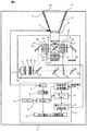
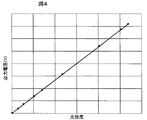
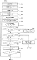
図1は本発明を適用した第1の実施例を示す投射型表示装置の構成を示す図、図2は投射レンズの光軸に直交する断面を拡大し出射光側から見た図、図3は投射レンズを拡大し横から見た図、図4は表示領域内で画像光の光強度を変化させたときに乱反射光の光強度を検出器で検出した結果をグラフ化したものである。 FIG. 1 is a diagram showing a configuration of a projection display device according to a first embodiment to which the present invention is applied, FIG. 2 is an enlarged view of a section orthogonal to the optical axis of the projection lens, and is a diagram seen from the outgoing light side, FIG. FIG. 4 is a graph showing the result of detecting the light intensity of irregularly reflected light with a detector when the light intensity of the image light is changed in the display area.
図1において、1は投射型表示装置であり、光学部2と信号処理部3とを含む。最初に、図1,図2,図3,図4を用いて、光学部2について説明する。図1において、光源20から出た光束は複数のレンズセル(図示せず)からなる第1レンズアレイ21に入射する。第1レンズアレイ21に入射した光束は各レンズセルで複数の光束に分割され、複数のレンズセル(図示せず)からなる第2レンズアレイ22のそれぞれ対応したレンズセル(図示せず)近傍に2次光源像を形成する。第2レンズアレイ22は、第1レンズアレイの各レンズセル像を合焦レンズ24とコンデンサレンズ27,32とリレーレンズ36,38,40とともに表示デバイス29,34,42上に重畳して結像させ、均一な照明を行う。
In FIG. 1,
このとき、第2レンズアレイ22を出射した光束は、偏光ビームスプリッタ−23により偏光がそろえられる(例えばS偏光)。また、合焦レンズ24を出射した白色光は、色分離手段としてのダイクロイックミラー25,31と、光路を折り曲げる反射ミラー26,37,39の作用により、それぞれ各色対応(ここでは、赤色,緑色,青色)の表示デバイス29,34,42(ここでは透過型液晶パネル)に分離されて導かれる。また、コントラストを向上させるために、表示デバイス29,34,42の前後に入射側偏光板28,33,41と出射側偏光板30,35,43が配置されている。
At this time, the light beams emitted from the second lens array 22 are aligned by the polarization beam splitter 23 (for example, S-polarized light). The white light emitted from the focusing lens 24 corresponds to each color (here, red, green, and red) by the action of the dichroic mirrors 25 and 31 as color separation means and the reflection mirrors 26, 37, and 39 that bend the optical path.
表示デバイス29,34,42にそれぞれ入射した色光は、各表示デバイスで後述する表示デバイス駆動回路からの駆動信号(電圧)に基づいて光強度変調されて、光学像が形成され、合成プリズム44により色合成されてカラー光学像とされ、該カラー光学像は投射レンズ15で拡大されてスクリーン45上に投射される。
The color lights respectively incident on the
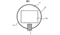
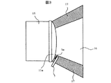
投射レンズ15からの出射光(投射光)は、図2,図3に示されるように、その光束断面が表示デバイスの表示領域(図示せず)と相似な矩形状領域(以下、この領域も「表示領域」と称する)16aであるスクリーン45上で光学像を形成する画像光16と、画像光16の周囲に形成される乱反射光17とからなる。乱反射光17は投射レンズ15内でレンズの表面や鏡筒151の面等で反射されて生じた光である。この乱反射光17は、スクリーン45の有効(表示)領域外に投影される。そして、投射レンズ15の出射側レンズ15a近傍には、明るさ(輝度)を検出する検出器5が配設されている。検出器5は、図3から明らかなように、周囲光の影響を低減するために、その受光部5aが投射レンズ15の出射側レンズ15aの向きに取り付けられ、表示領域16aの周囲に現れる乱反射光(斜線部)17の光強度を検出する構成になっている。
As shown in FIGS. 2 and 3, the outgoing light (projection light) from the
図4に、画像光領域内で画像光の光強度を変化させたときに検出器5で検出される乱反射光の光強度特性の一例を模式的に示す。この光強度特性から画像光領域内の光強度とその周辺に現れる乱反射光に相関関係があることが導かれる。つまり、画像光に影響を及ぼさない(例えば、検出器5の影が生じない)ように、表示領域外に検出器5を配置し、検出器5で乱反射光17を検出すれば、検出値と画像光の光強度との間に相関があるので、投射型表示装置の最初の使用開始時の検出器5による初期検出値と、経時変化後の検出値とを比較すれば、初期値に対する光強度(輝度)低下量の変化(後述するが、本発明では初期検出値に対する経時変化後の検出値の比を用いる)を知ることができる。
FIG. 4 schematically shows an example of the light intensity characteristic of the irregularly reflected light detected by the detector 5 when the light intensity of the image light is changed in the image light region. From this light intensity characteristic, it is derived that there is a correlation between the light intensity in the image light region and the irregularly reflected light appearing around it. That is, if the detector 5 is arranged outside the display area so as not to affect the image light (for example, the shadow of the detector 5 does not occur) and the irregularly reflected
次に、図1を用いて、信号処理部3について説明する。図1において、信号処理部3は、入力された映像信号に必要な信号処理を行う映像信号処理回路7と、信号処理された映像信号を記憶するためのフレームメモリ14と、フレームメモリ14から出力された映像信号を基に表示デバイス29,34,42をそれぞれ駆動する駆動信号を生成する表示デバイス駆動回路13と、表示デバイス駆動回路13から出力される最大諧調値(例えば映像信号が8ビットの場合には、階調値255)に対応した出力電圧を調整する出力電圧レベル調整回路12と、光束の明るさ(輝度)を検出する検出器5から出力される電流または電圧を増幅するアンプ8と、アンプ8の出力をデジタルデータに変換するA/D変換回路9と、不揮発性のメモリ10と、図示しないROMに格納されたプログラムに従って投射型表示装置全体の制御を行う演算制御手段(以下、「マイコン」と記す)11で構成されている。
Next, the
メモリ10には、光源,偏光板や表示デバイスなどの光学部品の経時変化で生じる輝度低下の変化を測定するための表示パターン(ビットマップパターン)が予め記憶されており、また、輝度低下の変化の基準値となる初期値が記憶される。
The
通常の映像表示の場合、信号処理部3に入力された映像信号6は映像信号処理回路7で所定の信号処理がなされ、フレームメモリ14に記憶される。表示デバイス駆動回路13は、フレームメモリ14から入力された映像信号を基に、表示デバイス29,34,42をそれぞれ駆動する駆動信号を生成し、各表示デバイスを駆動して、それぞれの光の透過率あるいは反射率を該駆動信号電圧に応じて変化させ、各表示デバイス上に該表示デバイスに対応した色光の光学像を形成させる。この時、表示デバイス駆動回路13から出力される最大諧調値に対応した出力電圧Vw(以下、この電圧を疑義が生じない限り、「基準出力電圧」と称する)が出力電圧レベル調整回路12で規定されるので、表示デバイス駆動回路13から出力される任意諧調値の映像信号の出力電圧は、基準出力電圧Vwを重み係数とした出力となる。従って、表示デバイス上に形成される光学像の明るさ(輝度)は基準出力電圧Vwにより左右されることになる。つまり、基準出力電圧Vwを調整することにより、明るさを変えることができる。なお、ここでは、基準出力電圧Vwが大きい程明るくなるものとする。
In the case of normal video display, the video signal 6 input to the
通常、Vwで透過率100%となるように設定するが、以下の説明では、使用開始時(工場出荷時)に、Vwで透過率100%以下にし、経時変化で生じる輝度低下を、Vwを大きくして補正できるようにしているものとする。ただし、本発明はこれに限定されるものではない。 Normally, the transmittance is set to be 100% at Vw. However, in the following description, at the start of use (at the time of shipment from the factory), the transmittance is reduced to 100% or less at Vw. It is assumed that it can be corrected by increasing it. However, the present invention is not limited to this.
一方、光強度を検出する場合には、マイコン11はメモリ10から所定の表示パターンを読み出し、フレームメモリ14上に書込み、表示デバイス駆動回路を介して各表示デバイス上に所定の表示パターンを表示し、スクリーン45に投射させる。投射レンズ15の出射側近傍に配設された検出器5は、投射レンズ15から出射される光(乱反射光)を検出して、例えば電圧を発生させ、該電圧はA/D変換器でデジタル量に変換され、マイコン11に入力される。マイコン11は、初期値の測定の場合には、入力された測定データをメモリ10に初期値として記憶させ、以降の経時変化の影響による輝度低下の調整の場合には、経時変化で生じる輝度低下の影響を低減するために、初期値からの変化量(後述するが、本発明では変化比)を求め、その変化量に基づいて、出力電圧レベル調整回路12で、表示デバイス駆動回路13から表示デバイスに出力される駆動信号の基準出力電圧を調整する。これらの一連の処理は、フローチャート図を用いて詳細に後述する。なお、投射型表示装置の使用開始時には、表示デバイス駆動回路13から出力される基準出力電圧は、出力電圧レベル調整回路12で所定の出力電圧に設定されているものとする。
On the other hand, when detecting the light intensity, the microcomputer 11 reads a predetermined display pattern from the
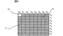
図5は、予めメモリ10に格納されている、経時変化で生じる輝度低下の変化を測定する際に用いる表示パターン(ビットマップパターン)の一例である。表示デバイスの矩形状の表示領域を、図5のように、8行(行V0〜V7)8列(列H0〜H7)のセル(小領域)52に64分割し、(Hi列,Vj行)のセルをHiVjで表示するものとすれば、メモリ10には、各セルHiVj(i,j:0〜7)部のみを白(100%)表示させ、他のセルは黒(0%)表示させる64通りの表示パターンが格納されている。図5では、セルH0V0が白表示部分50で、他のセルは黒表示部分51である。マイコン11は表示パターンを表示する場合、メモリ10に格納されている表示パターンの内の一つを適宜読み出し、フレームメモリ14に書込み、表示デバイスにパターン表示を行わせる。なお、以下セルHiVj部のみを白表示させる表示パターンをPijで表すものとする。
FIG. 5 is an example of a display pattern (bitmap pattern) that is stored in advance in the
ところで、図1において、光源20は光を投射するものを意味しており、ランプやLED等でもよく、限定するものではない。また、光学部2の構成は偏光ビームスプリッター、偏光板、レンズ、表示デバイスなど必ずしも図1のような構成にする必要はない。用いる表示デバイスに合わせて、適宜その構成を変更してもよい。
By the way, in FIG. 1, the
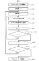
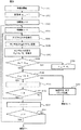
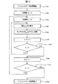
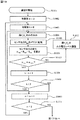
以下、本実施例による経時変化で生じる輝度低下の調整処理の動作について、フローチャートを用いて詳細に説明する。まず、リファレンスデータ(初期値)の取得手順について説明する。図6はリファレンスデータ(初期値)取得手順のフローチャートである。 Hereinafter, the operation of the adjustment process of the luminance reduction caused by the change with time according to the present embodiment will be described in detail using a flowchart. First, reference data (initial value) acquisition procedures will be described. FIG. 6 is a flowchart of a reference data (initial value) acquisition procedure.
図6において、ステップ(以下、「S」と省略する)101でリファレンスデータの取得を開始すると、まず初期値j=0(S102),i=0(S103)とし、S104に進み、図5に示すように、64セルに分割した表示デバイスの表示領域の内セルHiVjのみを白表示にした表示パターンPijをメモリ10から読み出し、フレームメモリ14に書込み、該表示パターンPijを表示デバイス上に形成し、投射レンズ15でスクリーン45に投射させる。そして、投射レンズ15の出射側レンズ15a近傍に配設された検出器5から得られる乱反射光17の光強度を検出し、そのときの検出器5の検出出力値(以下、「センサ出力値」と称する)Rijを表示パターンPijに対応させてメモリ10に記憶する(S105)。S106では現在値iに+1し、S107でその加算値が表示領域の列数8より小さいかを判定する。S107の判定結果がYESであれば、Vj行でのデータ取得が終わってないので、S104に戻り、以下、Vj行の全てのセルHiVj(i:0〜7)でのデータ取得が終わるまでS104〜S107の処理を繰り返す。
In FIG. 6, when reference data acquisition is started in step (hereinafter abbreviated as “S”) 101, initial values j = 0 (S102) and i = 0 (S103) are set, and the process proceeds to S104. As shown, the display pattern P ij in which only the cell H i V j in the display area of the display device divided into 64 cells is displayed in white is read from the
S107でNOであれば、Vj行の全てのセルでのデータ取得が終わったので、次の行のデータ取得を行うために、S108で現在値jに+1する。そして、S109でその加算値が表示領域の行数8より小さいかを判定し、その判定結果がYESであれば、全ての行でのデータ取得が終わってないので、S103に戻り、以下、全ての行でのデータ取得が終わるまでS103〜S109の処理を繰り返す。S109でNOであれば、すべての行すなわち全てのセルでのデータ取得が終わったので、リファレンスデータ取得処理を終了する(S110)。
If NO in S107, the data acquisition for all the cells in the Vj row is completed, so that the current value j is incremented by 1 in S108 in order to acquire the data for the next row. Then, in S109, it is determined whether or not the added value is smaller than the
以上の処理で得られた、つまりセルHiVjのみ白表示でその他の全てのセルを黒表示として得られた64個のデータ(R00からR77)をリファレンスデータとする。 The 64 data (R 00 to R 77 ) obtained by the above processing, that is, obtained by displaying only the cells H i V j in white and all the other cells in black are used as reference data.
なお、本実施例では、64分割の表示パターンについて説明したが、表示パターンの分割数詳細に関してはシステムや目的に応じて調整するものであり、分割数を増やすほど表示領域内を細かく把握でき検出時間が増えるが、本実施例の表示パターンの分割数に限定するものではない。 In this embodiment, the display pattern of 64 divisions has been described. However, the details of the number of divisions of the display pattern are adjusted according to the system and purpose, and the display area can be grasped in detail as the division number is increased. Although time increases, it is not limited to the division number of the display pattern of a present Example.
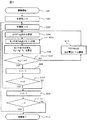
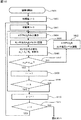
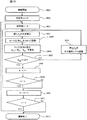
次に、経時変化で生じる輝度低下の調整処理の動作について説明する。図7は表示領域を分割したセル毎の調整手順のフローチャートである。 Next, the operation of the adjustment process for the luminance decrease caused by the change with time will be described. FIG. 7 is a flowchart of the adjustment procedure for each cell obtained by dividing the display area.
図7において、S201で調整を開始すると、まず初期値j=0(S202)、i=0(S203)とし、S204に進む。S204では、図6のS104と同様にセルHiVjのみを白表示にした表示パターンPijを出力し、投射型表示装置1で表示させ、検出器5から得られる乱反射光17の光強度を検出し、そのときの検出器5のセンサ出力値Aijを表示パターンPijに対応させてメモリ10に記憶する(S205)。
In FIG. 7, when adjustment is started in S201, initial values j = 0 (S202) and i = 0 (S203) are set, and the process proceeds to S204. In S204, as in S104 of FIG. 6, a display pattern Pij in which only the cell H i V j is displayed in white is output, displayed on the
次に、S206で、セルHiVjにおける経年変化による輝度低下の変化量を初期値であるリファレンスデータRijに対するAijの比で定義し、マイコン11はメモリ10からRijとAijを読み出し、該変化量αij=Aij/Rijを算出する。そして、S207で、変化量αijが1であるか判定を行う。S207でNOであれば輝度変化が大きいので、S212に行き、表示デバイス駆動回路13の出力電圧を出力電圧レベル調整回路12で、表示デバイス上の光学像の明るさを明るくする方向に調整し、S204〜S207−S212のループ処理を繰り返し行い、変化量αij=1となるようにする。なお、用いた表示パターンの白は100%レベルなので、表示デバイス駆動回路13の出力電圧は最大階調値に対応した基準出力電圧となるが、αij=1となれば、初期の明るさと等しい明るさを実現できる基準出力電圧となる。
Next, in S206, the amount of change in luminance reduction due to secular change in the cell H i V j is defined by the ratio of A ij to the reference data R ij that is the initial value, and the microcomputer 11 determines R ij and A ij from the
S207でYESであれば、そのセルでは輝度低下(変化)はない(あるいはαij=1と調整できた)ので、その時の表示デバイス駆動回路13からの出力電圧(基準出力電圧)を表示パターンPijに対応させてメモリ10に記憶し、S208に進み、現在値iに+1し、S209でその加算値が表示領域の列数8より小さいかを判定する。S209の判定結果がYESであれば、Vj行での調整が終わってないので、S204に戻り、以下、Vj行の全てのセルHiVj(i:0〜7)での調整が終わるまでS204〜S209の処理を繰り返す。
If YES in S207, there is no luminance drop (change) in the cell (or adjustment can be made to α ij = 1), and the output voltage (reference output voltage) from the display device drive circuit 13 at that time is displayed as the display pattern P. Store in the
S209でNOであれば、Vj行の全てのセルでの調整が終わったので、次の行の調整を行うために、S210で現在値jに+1する。そして、S211でその加算値が表示領域の行数8より小さいかを判定し、の判定結果がYESであれば、全ての行でのデータ取得が終わってないので、S203に戻り、以下、全ての行でのデータ取得が終わるまでS203〜S211の処理を繰り返す。S211でNOであれば、すべての行すなわち全てのセルでの調整が終わったので、調整処理を終了する(S213)。
If NO in S209, the adjustment in all the cells in the Vj row is completed, so that the current value j is incremented by 1 in S210 in order to adjust the next row. Then, in S211, it is determined whether or not the added value is smaller than the
この調整処理で得られた、全ての64分割したセルHiVjに対応したデバイス駆動回路13からの出力電圧(基準出力電圧)はメモリ10に記憶され、以後、これらの基準出力電圧Vmaxij(i,j:0〜7)を基に、表示領域の明るさを初期の明るさに設定できる。
The output voltage (reference output voltage) from the device drive circuit 13 corresponding to all the 64 divided cells H i V j obtained by this adjustment processing is stored in the
以上述べたように、本実施例によれば、光学部品の経時変化により輝度低下(輝度変化)が生じても、輝度低下(輝度変化)がなくなるように調整できる。その際、検出器を投射レンズの出射側レンズ近傍に設けたため、光源のみならず、光源から投射レンズまでの光路上に配設された光学部品の経時変化の影響を含めることができる。また、検出器の受光部を投射レンズの出射側レンズ側に向けるので、周囲光の影響を軽減できる。また、検出器を乱反射光領域に設置し、輝度検出を乱反射光を用いて行っているので、スクリーン上に検出器の影が映るなどの副作用もない。また、分割の表示パターンを用いて光強度を検出するので、画像光を部分的に検出でき、輝度むらも低減できる。 As described above, according to the present embodiment, it is possible to make an adjustment so that a luminance decrease (luminance change) is eliminated even when a luminance decrease (luminance change) occurs due to a change with time of the optical component. At this time, since the detector is provided in the vicinity of the exit side lens of the projection lens, it is possible to include not only the light source but also the influence of changes over time of the optical components disposed on the optical path from the light source to the projection lens. In addition, since the light receiving portion of the detector is directed toward the exit lens side of the projection lens, the influence of ambient light can be reduced. Further, since the detector is installed in the irregular reflection light region and the luminance detection is performed using the irregular reflection light, there is no side effect such as the shadow of the detector being reflected on the screen. Further, since the light intensity is detected using the divided display pattern, the image light can be partially detected, and the luminance unevenness can be reduced.
なお、上記では、図7のS207の判定をαij=1としたが、これに限定されるものではなく、αijが1を中心に所定の近傍範囲内となるようにしてもよいことはいうまでもない。また、表示パターンの白レベルを100%としたが、本発明は変化量が等しくなるように調整するのであるから、これに限定されるものではなく、任意のレベル例えば80%白であってもよい。 In the above description, the determination in S207 of FIG. 7 is α ij = 1, but the present invention is not limited to this, and α ij may be within a predetermined vicinity range centering on 1. Needless to say. Further, although the white level of the display pattern is set to 100%, the present invention is adjusted so that the amount of change is equal. Therefore, the present invention is not limited to this, and any level such as 80% white may be used. Good.
第1の実施例では、説明を容易とするために、経時変化による輝度低下を元の輝度に戻せる(補正できる)ものとしたが、輝度低下が大きい場合には、補正ができない場合も考えられる。この事を考慮した第2の実施例について以下述べる。なお、本実施例のブロック構成は、第1の実施例と同じであり、その構成の詳細については、その説明を省略する。 In the first embodiment, for ease of explanation, it is assumed that the luminance decrease due to the change with time can be returned (corrected) to the original luminance. However, when the luminance decrease is large, there is a case where the correction cannot be performed. . A second embodiment in consideration of this will be described below. The block configuration of the present embodiment is the same as that of the first embodiment, and the details of the configuration are not described here.
図8,図9,図10は第2の実施例を示す調整手順のフローチャートである。 8, FIG. 9 and FIG. 10 are flowcharts of the adjustment procedure showing the second embodiment.
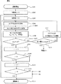
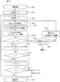
第2の実施例は、第1の実施例を示す図7において、判定処理S214を追加したものであり、第1の実施例と同じS201〜S212の処理については、その説明を省略し、S214以降の処理について、以下説明する。 In the second embodiment, a determination process S214 is added to FIG. 7 showing the first embodiment, and the description of the same processes of S201 to S212 as in the first embodiment is omitted. The subsequent processing will be described below.
図8において、S214では、対象セルHiVjにおける表示デバイス駆動回路13からの出力電圧が最大であるか判定する。なお、ここでいう最大出力電圧とは、表示デバイス(ここでは透過型液晶パネル)の光の透過率が100%となる時の電圧である。最大でなければ、出力電圧レベル調整回路12で出力電圧を上げることができるので、S212に行き出力電圧の調整を行う。最大であれば調整できないので、図9の調整2のS301に行き、調整2を開始する。
In FIG. 8, in S214, it is determined whether the output voltage from the display device drive circuit 13 in the target cell H i V j is the maximum. Note that the maximum output voltage here is a voltage when the light transmittance of the display device (here, the transmissive liquid crystal panel) becomes 100%. If it is not the maximum, the output voltage
調整2は64個のセルの内で、最も変化が大きいつまり変化量αij=Aij/Rijが最も小さい(暗い)ものを算出する処理である。
The
図9において、調整2を開始すると、初期値αmin=1(S302),j=0(S303),i=0(S304)とし、セルHiVjのみを白表示にした表示パターンPijを出力し、投射型表示装置1で表示させ(S305)、検出器5から得られる乱反射光17の光強度を検出し、そのときの検出器5のセンサ出力値Aij をメモリ10に記憶する(S306)。次に、S307で、メモリ10からRijとAijを読み出し、変化量αij=Aij/Rijを算出し、S308でαij≧αminであるか判定する。NOならS309へ進み、αmin=αijとしてS310に進み、YESであればそのままS310に進む。S310では、画像光が暗くなりすぎ、光源20の交換が必要と判断される変化量(ここではこの値を例えば0.8とする)よりαminが大きいか判定する。
In FIG. 9, when the
S310でNOであれば、S315で光源20交換などのアラームを行い(例えば「ランプ交換」の表示を行い)、光源交換を促し、S213へ行き、調整処理を終了する。
If NO in S310, an alarm such as replacement of the
S310でYESであれば、S311に進み、現在値iに+1し、S312でその加算値が表示領域の列数8より小さいかを判定する。S312の判定結果がYESであれば、Vj行での調整が終わってないので、S305に戻り、以下、Vj行の全てのセルHiVj(i:0〜7)でのデータ取得が終わるまでS305〜S312の処理を繰り返す。S312でNOであれば、Vj行の全てのセルでの調整が終わったので、次の行の調整を行うために、S313で現在値jに+1する。そして、S314でその加算値が表示領域の行数8より小さいかを判定し、その判定結果がYESであれば、全ての行でのデータ取得が終わってないので、S304に戻り、以下、全ての行でのデータ取得が終わるまでS304〜S314の処理を繰り返す。S314でNOであれば、すべての行すなわち全てのセルでの調整が終わった、すなわちターゲットとするαminの値が算出されたことになり、図10の調整3のS401へ進み、調整3を開始する。
If “YES” in S310, the process proceeds to S311 to increment the current value i by 1, and it is determined in S312 whether the added value is smaller than the
調整3は64個のセルの変化量を調整2で算出されたαminに設定する処理である。
図10において、調整3を開始すると、j=0(S402),i=0(S403)とし、セルHiVjのみを白表示にした表示パターンPijを出力し、投射型表示装置1で表示させ(S404)、検出器5から得られる乱反射光17の光強度を検出し、そのときの検出器5のセンサ出力値Aij をメモリ10に記憶する(S405)。次に、S406で変化量αij=Aij/Rijを算出し、S407でαij=αminであるか判定する。NOであればS412に進み、表示デバイス駆動回路13の出力電圧を出力電圧レベル調整回路12で調整し、S404〜S407−S412のループ処理を繰り返し行い、変化量αij=αminとなるようにする。
In FIG. 10, when
S407でYESとなれば、その時の表示デバイス駆動回路13からの出力電圧(基準出力電圧)をセルHiVjに対応させてメモリ10に記憶し、全てのセルHiVj(i:0〜7,j:0〜7)について、iおよびjを変えて、変化量αij=αminと設定する処理を行い(S408〜S411)、全てのセルに対する設定処理(調整3)が完了すると、S213に行き、調整処理を終了する。
If YES in S407, is stored in the
以上述べたように、本実施例によれば、第1の実施例に記載の効果に加えて、経時変化による輝度低下を元の輝度に戻せない(補正できない)場合には、各セルでの輝度(光強度)の変化量が同じとなるように調整することにより、輝度ムラをなくし、経時変化による映像の変化を低減することが可能である。また、輝度(光強度)の変化が大きく、その変化量(比)の値が小さい場合には、ランプの交換を促すようにしたので、メンテナンスも容易となる。 As described above, according to the present embodiment, in addition to the effects described in the first embodiment, when the luminance decrease due to the change over time cannot be returned to the original luminance (cannot be corrected), By adjusting the amount of change in luminance (light intensity) to be the same, it is possible to eliminate unevenness in luminance and reduce changes in video due to changes over time. In addition, when the change in luminance (light intensity) is large and the amount of change (ratio) is small, the lamp is urged to be replaced, so that maintenance is facilitated.
本実施例では、ターゲットの変化量をαminとして表示領域を均一に調整する方法を説明したが、αminは調整する目的に応じて調整するのものであり、特にαmin=0.8に限定するものではない。 In the present embodiment, the method of uniformly adjusting the display area by setting the target change amount as α min has been described. However, α min is adjusted according to the purpose of adjustment, and in particular, α min = 0.8. It is not limited.
また、図8のS214の判定処理で、YESの場合には、ランプ交換表示をして、直ちに、調整処理を終了するようにしてもよい。 Further, in the determination process of S214 in FIG. 8, if YES, a lamp replacement display may be displayed and the adjustment process may be immediately terminated.
また、図9のS315では、「ランプ交換」の表示を行い、調整処理を終了するとしたが、これに限定されるものではなく、経時変化によって輝度低下が生じる表示デバイス,光学部品等も交換するように促し、調整処理を終了するようにしてもよい。 In S315 of FIG. 9, “Lamp replacement” is displayed and the adjustment process is terminated. However, the present invention is not limited to this, and a display device, an optical component, or the like that decreases in luminance due to a change with time is also replaced. The adjustment process may be terminated.
次に、第3の実施例について説明する。第1の実施例では、表示デバイスの矩形状の表示領域を図5のように8行,8列の64セルに分割したが、本実施例では、分割数を少なくして、高速かつ簡易的に調整可能にしたものである。なお、本実施例のブロック構成は、第1の実施例と同じであり、その構成の詳細については、その説明を省略する。 Next, a third embodiment will be described. In the first embodiment, the rectangular display area of the display device is divided into 64 cells of 8 rows and 8 columns as shown in FIG. 5. However, in this embodiment, the number of divisions is reduced to achieve high speed and simplicity. Can be adjusted. The block configuration of the present embodiment is the same as that of the first embodiment, and the details of the configuration are not described here.
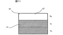
図11は、本実施例による予めメモリ10に格納されている、経時変化で生じる輝度低下の変化を測定する際に用いる表示パターン(ビットマップパターン)の一例である。図11のように、表示デバイスの矩形状の表示領域を3行(U0〜U2)の小領域(セル)62に分割し、各セルをUiで表示するものとすれば、メモリ10には、各セルUi(i:0〜2)部のみを白表示させ、他のセルは黒(0%)表示させる3通りの表示パターンが格納されている。図11では、セルU0が白表示部分60で、他のセルU1,U2は黒表示部分61である。
FIG. 11 is an example of a display pattern (bitmap pattern) that is stored in advance in the
以下、本実施例の動作について説明する。図12はリファレンスデータ取得手順のフローチャートである。 Hereinafter, the operation of this embodiment will be described. FIG. 12 is a flowchart of the reference data acquisition procedure.
図12において、S501でリファレンスデータの取得を開始すると、まず初期値i=0(S502)とし、S503に進み、図11に示すように、セルUiのみを白表示にした表示パターンPiを出力し、投射型表示装置1で表示させる。そして、検出器5から得られる乱反射光17の光強度を検出し、そのときの検出器5の検出出力値であるセンサ出力値Riをメモリ10に記憶する(S504)。以上のようにして、表示パターンP0を用いたリファレンスデータ取得ができる。以下、S505,S506でi=1,i=2として表示パターンP1,P2を用いたリファレンスデータ取得を行い、リファレンスデータ取得を終了する(S507)。
In FIG. 12, when the acquisition of reference data is started in S501, first, the initial value i = 0 (S502), and the process proceeds to S503. As shown in FIG. 11, a display pattern P i in which only the cell U i is displayed in white is displayed. The data is output and displayed on the
以上の処理で得られた、つまりセルViのみ白表示でその他の全てのセルを黒表示として得られた3個のデータ(R0からR2)をリファレンスデータとする。
Obtained in the above process, it is referred to as reference data to all cells other in white display only That cell V i (R 2 from
なお上記では、3分割の表示パターンについて説明したが、これに限定されるものではなく、必要に応じて適宜変更できることはいうまでもない。 In the above description, the three-divided display pattern has been described. However, the present invention is not limited to this, and it is needless to say that the display pattern can be changed as needed.
次に、経時変化で生じる輝度低下の調整処理の動作について説明する。図13は調整手順のフローチャートである。 Next, the operation of the adjustment process for the luminance decrease caused by the change with time will be described. FIG. 13 is a flowchart of the adjustment procedure.
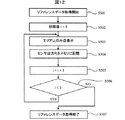
図13において、S601で調整を開始すると、まず初期値i=0(S602)とし、S603に進む。S603では、セルUiのみを白表示にした表示パターンPiを出力し、投射型表示装置1で表示させ、検出器5から得られる乱反射光17の光強度を検出し、そのときの検出器5のセンサ出力値Ai をメモリ10に記憶する(S604)。
In FIG. 13, when the adjustment is started in S601, the initial value i = 0 is first set (S602), and the process proceeds to S603. In S603, the display pattern P i in which only the cell U i is displayed in white is output, displayed on the
次に、S605で、メモリ10からRiとAiを読み出し、変化量αi=Ai/Riを算出する。次に、S606で現在値iに+1し、S607でその加算値が表示領域の行数3より小さいかを判定する。S607の判定結果がYESであれば、全ての行での測定が終わってないので、S603に戻り、以下、全ての行でのデータ取得が終わるまでS603〜S607の処理を繰り返す。
Next, in S605, R i and A i are read from the
S607でNOであれば、すべての行すなわち全てのセルでの測定が終わったので、S608で表示画面の平均の変化量α=Σαi/3を算出する。次に、S609で平均変化量αが1.0であるか判定を行い、NOであればS610に行き、表示領域全体において、表示デバイス駆動回路13の出力電圧を、出力電圧レベル調整回路12で、平均変化量αが1.0になるように所定の電圧ステップで調整し、そして、S603〜S609−S610のループ処理をα=1となるまで繰り返す。
If NO in S607, the measurement in all rows, that is, all cells is completed, and in S608, the average change amount α = Σα i / 3 of the display screen is calculated. Next, in S609, it is determined whether the average change amount α is 1.0. If NO, the process goes to S610, and the output voltage of the display device drive circuit 13 is output by the output voltage
平均変化量α=1.0に調整できたら、調整処理を終了する(S611)。 If the average change amount α = 1.0 can be adjusted, the adjustment process is terminated (S611).
以上により、第1の実施例と同様な効果を得ながら、経時変化による映像全体の輝度変化を簡易的にかつ短時間の処理で低減することが可能である。 As described above, while obtaining the same effect as that of the first embodiment, it is possible to reduce the luminance change of the entire image due to the change with time in a simple and short process.
なお、図13のS609ではα=1.0としたが、これに限定されるものではなく、平均変化量αが1を中心に所定の近傍範囲内となるようにしてもよいことはいうまでもない。 Note that α = 1.0 in S609 in FIG. 13, but the present invention is not limited to this, and it goes without saying that the average change amount α may be within a predetermined vicinity range centering on 1. Nor.
また、本実施例では、S610で、表示領域全体における表示デバイス駆動回路13の出力電圧を、出力電圧レベル調整回路12で、平均変化量αが1.0になるように調整したが、これに限定されるものではなく、光源20の明るさを制御する光源制御手段(図示せず)を備え、該光源制御手段で光源20の明るさを上げて、平均変化量αが1.0になるように調整してもよい。光源制御手段で光源20の明るさを調整すると、容易に表示領域全体の明るさを平均的に上げることができる。
In this embodiment, in S610, the output voltage of the display device drive circuit 13 in the entire display area is adjusted by the output voltage
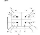
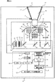
本発明は、投射型表示装置を複数台配列して表示を行う所謂マルチスクリーン装置にも適用できる。以下、本発明をマルチスクリーン装置に用いた第4の実施例について説明する。図14は第4の実施例を示すマルチスクリーン装置の模式構成図、図15は第4の実施例を示す一レファレンスデータ取得処理、図16は第4の実施例を示す一調整処理である。 The present invention can also be applied to a so-called multi-screen device that performs display by arranging a plurality of projection display devices. Hereinafter, a fourth embodiment in which the present invention is used in a multi-screen device will be described. FIG. 14 is a schematic configuration diagram of the multi-screen apparatus showing the fourth embodiment, FIG. 15 is a reference data acquisition process showing the fourth embodiment, and FIG. 16 is an adjustment process showing the fourth embodiment.
図14において、マルチスクリーン装置は例えば図1で示される4台の投射型表示装置が2列(H0,H1)2行(V0,V1)に配列されて構成されている。便宜上、列,行の交点の投射型表示装置を符号1km,その表示面を符号HkVm,投射型表示装置1kmに設けられた検出器の符号を5kmで示すものとする。また、4台の投射型表示装置の内、マルチスクリーン装置全体の制御を行うマスター機器が例えば投射型表示装置100であり、他の投射型表示装置110,101,111はスレーブ機器とする。従って、マルチスクリーン装置は投射型表示装置100のマイコン1100で制御線70を介して制御される。各投射型表示装置1kmの構成は図1に同じであり、その詳細な説明を省略する。また、各投射型表示装置1kmの構成要素を示す場合には、構成要素の符号に添え字kmを付して示すものとする。
In FIG. 14, the multi-screen device is configured by arranging, for example, four projection display devices shown in FIG. 1 in two columns (H 0 , H 1 ) and two rows (V 0 , V 1 ). For the sake of convenience, the projection type display device at the intersection of columns and rows is denoted by
まず、リファレンスデータ取得処理について、図15を用いて述べ、次に調整処理について図16を用いて説明する。本実施例ではマルチスクリーン装置を構成する投射型表示装置ごとに第3の実施例に用いた調整アルゴリズムを使うが、これに限定されるものではない。 First, reference data acquisition processing will be described with reference to FIG. 15, and then adjustment processing will be described with reference to FIG. In this embodiment, the adjustment algorithm used in the third embodiment is used for each projection display device constituting the multi-screen device, but the present invention is not limited to this.
図15において、S701でリファレンスデータの取得を開始すると、マスター機器の投射型表示装置100のマイコン1100は、まず初期値m =0(S702),k=0(S703)とし、S704に進み、投射型表示装置1km(表示面HkVm)のマイコン11kmに対してデータ取得を指示する。指示されたマイコン11kmは、第3の実施例でのリファレンス取得アルゴリズムに従い、白表示を行い、検出器5kmにより乱反射光17kmの光強度を検出し、そのときのセンサ出力値Skm をメモリ10kmに記憶する(S705)。そして、マスター機器のマイコン1100にデータ取得したことを連絡する。すると、マスター機器のマイコン1100は、S706で現在値kに+1し、S707でその加算値がマルチスクリーン装置を構成する投射型表示装置の列数2より小さいかを判定する。S707の判定結果がYESであれば、Vm行でのデータ取得が終わってないので、S104に戻り、以下、Vm行の全ての投射型表示装置1km(k:0,1)でのデータ取得が終わるまでS704〜S707の処理を繰り返す。
15, when starting the acquisition of the reference data in S701, the microcomputer 11 00 of the projection type display device 1 00 of the master device, first the initial value m = 0 (S702), k = 0 and (S703), the process proceeds to S704 The microcomputer 11 km of the projection display device 1 km (display surface H k V m ) is instructed to acquire data. The instructed microcomputer 11 km performs white display according to the reference acquisition algorithm in the third embodiment, detects the light intensity of the irregularly reflected light 17 km by the detector 5 km , and obtains the sensor output value S km at that time. The data is stored in the memory 10 km (S705). Then, it notifies the master device microcomputer 1100 that the data has been acquired. Then, the microcomputer 11 00 of the master device, +1 to the current value k at S706, determines that or sum is the number of
S707でNOであれば、Vm行の全ての投射型表示装置でのデータ取得が終わったので、次の行のデータ取得を行うために、S708で現在値mに+1する。そして、S709でその加算値が行数2より小さいかを判定し、その判定結果がYESであれば、全ての行でのデータ取得が終わってないので、S703に戻り、以下、全ての行でのデータ取得が終わるまでS703〜S709の処理を繰り返す。S709でNOであれば、すべての行すなわち全ての投射型表示装置でのデータ取得が終わったので、リファレンスデータ取得処理を終了する(S710)。
If NO in S707, since the finished data acquisition in all of the projection type display device of the row V m, in order to perform the data acquisition for the next row is +1 to the current value m in S 708. Then, in S709, it is determined whether the added value is smaller than the number of
以上の処理で得られたリファレンスデータを基準に、次に述べる調整を行うことが可能である。 The adjustment described below can be performed on the basis of the reference data obtained by the above processing.
次に調整処理について図16を用いて説明する。図16において、S801で調整を開始すると、マスター機器の投射型表示装置100のマイコン1100は、まず初期値m=0(S802)、k=0(S803)とし、S804に進み、投射型表示装置1km(表示面HkVm)のマイコン11kmに対して経時変化後の調整を指示する。指示されたマイコン11kmは、第3の実施例での調整アルゴリズムに従い、白表示を行い、検出器5kmから得られる乱反射光17kmの光強度を検出し、そのときのセンサ出力値Bkmをメモリ10kmに記憶する(S805)。 Next, the adjustment process will be described with reference to FIG. 16, when adjustment is started in S801, the projection display device 1 00 of the microcomputer 11 00 of the master device, first the initial value m = 0 (S802), k = 0 and (S803), the process proceeds to S804, projection The microcomputer 11 km of the display device 1 km (display surface H k V m ) is instructed to adjust after aging. The instructed microcomputer 11 km performs white display according to the adjustment algorithm in the third embodiment, detects the light intensity of the diffusely reflected light 17 km obtained from the detector 5 km, and the sensor output value B km at that time Is stored in the memory 10 km (S805).
次に、S806で、マイコン11kmはメモリ10kmからSkmとBkmを読み出し、変化量αkm=Bkm/Skmを算出する。そして、S807で変化量αkmが1.0であるか判定を行う。S807でNOであればS812に行き、表示デバイス駆動回路13kmの出力電圧を出力電圧レベル調整回路12kmで、αkmが1.0となる方向に、調整し、S804〜S807−S802のループ処理を繰り返し行い、変化量αkm=1となるようにする。
Next, in S806, the microcomputer 11 miles reads out S km and B km from the memory 10 miles, calculates the amount of change α km = B km / S km . In step S807, it is determined whether the change amount α km is 1.0. If NO in S807, the process goes to S812, and the output voltage of the display device drive circuit 13 km is adjusted by the output voltage
S807でYESとなれば、当該投射型表示装置での調整が終了したので、マスター機器のマイコン1100にその連絡を行う。すると、マスター機器のマイコン1100は、S808に進み、現在値kに+1し、S809でその加算値が列数2より小さいかを判定する。S809の判定結果がYESであれば、Vm行での調整が終わってないので、S804に戻り、以下、Vm行の全ての投射型表示装置1km(k:0,1)での調整が終わるまでS804〜S809の処理を繰り返す。
If YES in S807, since the adjustment in the projection type display device has been finished, the contact to the microcomputer 11 00 of the master device. Then, the microcomputer 11 00 of the master device proceeds to S808, and +1 to the current value k, determines the whether sum is the number of
S809でNOであれば、Vm行の全ての投射型表示装置での調整が終わったので、次の行の調整を行うために、S810で現在値mに+1する。そして、S811でその加算値が行数2より小さいかを判定し、その判定結果がYESであれば、全ての行での投射型表示装置の調整が終わってないので、S803に戻り、以下、全ての行での投射型表示装置の調整が終わるまでS803〜S811の処理を繰り返す。S811でNOであれば、すべての行すなわち全ての投射型表示装置での調整が終わったので、調整処理を終了する(S813)。
If NO in S809, since the finished adjustment for all of the projection type display device of the row V m, in order to adjust the next line, it is +1 to the current value m at S810. Then, in S811, it is determined whether the added value is smaller than the number of
以上述べたように、本実施例によれば、マルチスクリーン装置を構成する各投射型表示装置の経時変化による輝度低下を低減することができるとともに、経時変化による輝度低下で生じる各投射型表示装置間の輝度ムラも低減することができる。 As described above, according to the present embodiment, it is possible to reduce the decrease in luminance due to the change over time of each projection type display device constituting the multi-screen device, and each projection type display device caused by the decrease in luminance due to the change over time. It is possible to reduce luminance unevenness in the meantime.
本実施例では4面の投射型表示装置のマルチスクリーン装置で説明したが面数に限定はない。さらに個々の投射型表示装置ごとに調整を行うので、アルゴリズムのように順番にリファレンスの取得および調整を行う必要はなく、同時に行うことができる。 In this embodiment, the multi-screen device of the four-surface projection type display device has been described, but the number of surfaces is not limited. Further, since the adjustment is performed for each projection display device, it is not necessary to sequentially acquire and adjust the reference as in the algorithm, and the adjustment can be performed simultaneously.
なお、本実施例では、投射型表示装置100をマスター機器,他の投射型表示装置110,101,111をスレーブ機器としたが、これに限定されるものではなく、全ての投射型表示装置100,110,101,111をスレーブ機器とし、これらの機器を外部のマスター機器が制御するようにしてもよいことはいうまでもない。
In this embodiment, the projection
また、本実施例では、第3の実施例に用いた調整アルゴリズムを用い、出力電圧レベル調整回路12kmで変化量αkmが1となるようにしたが、第3の実施例でも述べたように、出力電圧レベル調整回路12kmに代えて光源20kmの明るさを制御する光源制御手段を各投射型表示装置に備え、該光源制御手段で光源20kmの明るさを上げて、平均変化量αkmが1.0になるように調整してもよい。
In this embodiment, the adjustment algorithm used in the third embodiment is used so that the change amount α km becomes 1 in the output voltage
第4の実施例であるマルチスクリーン装置では、説明を容易とするために、経時変化による輝度低下を元の輝度に戻せる(補正できる)ものとしたが、輝度低下が大きい場合には、補正ができない場合も考えられる。この事を考慮した第5の実施例について以下述べる。なお、本実施例のマルチスクリーン装置の構成は、第4の実施例と同じであり、その構成の詳細については、その説明を省略する。 In the multi-screen device according to the fourth embodiment, it is assumed that the luminance decrease due to the change over time can be returned to the original luminance (can be corrected) for easy explanation. There are cases where it is impossible. A fifth embodiment in consideration of this will be described below. The configuration of the multi-screen device of the present embodiment is the same as that of the fourth embodiment, and the details of the configuration will be omitted.
図17,図18,図19は第5の実施例を示す調整手順のフローチャートである。第5の実施例は、第4の実施例を示す図16において、判定処理S814を追加したものであり、第4の実施例と同じS801〜S812の処理については、その説明を省略し、S814以降の処理について、以下説明する。 17, 18 and 19 are flowcharts of the adjustment procedure showing the fifth embodiment. In the fifth embodiment, a determination process S814 is added to FIG. 16 showing the fourth embodiment, and the description of the same processes in S801 to S812 as in the fourth embodiment is omitted. The subsequent processing will be described below.
図17において、S814では、対象投射型表示装置1kmにおける表示デバイス駆動回路13kmからの出力電圧が最大であるか判定する。最大でなければ、出力電圧レベル調整回路12kmで出力電圧を上げることができるので、S812に行き出力電圧の調整を行う。最大であれば図18の調整2’のS901に行き、調整2’を開始する。
In FIG. 17, in S814, it is determined whether the output voltage from the display device drive circuit 13 km in the target
調整2’はマルチスクリーン装置を構成する4つの投射型表示装置の内で、最も輝度(光強度)の変化が大きいつまり最も小さい(暗い)αkmを算出する処理である。
The
調整2’を開始すると、マスター機器の投射型表示装置100のマイコン1100は、まず、初期値αmin=1(S902),m=0(S903),k=0(S904)とし、S905に進み、対象の投射型表示装置1km(表示面HkVm)のマイコン11kmに対して変化量αkmの算出を指示する。これを受けた対象の投射型表示装置1kmのマイコン11kmは、第3の実施例での調整アルゴリズムに従い、白表示を行い、検出器5kmから得られる乱反射光17kmの光強度を検出し、そのときのセンサ出力値Bkmをメモリ10kmに記憶する(S906)。次に、S907で、マイコン11kmはメモリ10kmからSkmとBkmを読み出し、変化量αkm=Bkm/Skmを算出し、その算出結果をマスター機器のマイコン1100に送信する。マスター機器のマイコン1100は、S908で受信したαkmがαkm≧αminであるか判定する。NOならS909へ進み、αmin=αkmとしてS910に進み、YESであればそのままS910に進む。S910では、画像光が暗くなりすぎ、光源20kmの交換が必要と判断される変化量(ここではこの値を例えば0.8とする)よりαminが大きいか判定する。S910でNOであれば、S915で光源20km交換などのアラームを行い(例えば投射型表示装置1kmの「ランプ交換」の表示を行い)、光源交換を促し、S813へ行き、調整処理を終了する。
When starting the adjustment 2 ', the projection type display device 1 00 of the microcomputer 11 00 of the master device, first, an initial value α min = 1 (S902), m = 0 (S903), k = 0 and (S904), S905 Then, the microcomputer 11 km of the target projection display device 1 km (display surface H k V m ) is instructed to calculate the change amount α km . Receiving this, the microcomputer 11 km of the target
S910でYESであれば、S911に進み、現在値kに+1し、S912でその加算値が列数2より小さいかを判定する。S912の判定結果がYESであれば、Vm行での調整が終わってないので、S905に戻り、以下、Vm行の全ての投射型表示装置1km(k:0,1)での調整が終わるまでS905〜S912の処理を繰り返す。S912でNOであれば、Vm行の全ての投射型表示装置での調整が終わったので、次の行の調整を行うために、S913で現在値mに+1する。そして、S914でその加算値が行数2より小さいかを判定し、その判定結果がYESであれば、全ての行での調整が終わってないので、S904に戻り、以下、全ての行での調整が終わるまでS904〜S914の処理を繰り返す。S914でNOであれば、すべての行すなわち全ての投射型表示装置での調整が終わった、すなわちターゲットとするαminの値が算出されたことになり、マスター機器のマイコン1100は図19の調整3’のS1001へ進み、調整3’を開始する。
If “YES” in S910, the process proceeds to S911, the current value k is incremented by 1, and whether or not the added value is smaller than the number of
調整3’はマルチスクリーン装置を構成する投射型表示装置の変化量を調整2’で算出されたαminに設定する処理である。
The
図19において、調整3’を開始すると、マスター機器の投射型表示装置100のマイコン1100は、まず、初期値m=0(S1002),k=0(S1003)とし、S1004に進み、対象の投射型表示装置1km(表示面HkVm)のマイコン11kmに対して、変化量αkmの算出を指示するとともに、調整2’で算出したデータαminも送る。これを受けた対象の投射型表示装置1kmのマイコン11kmは、データαminをメモリ10kmに格納するとともに、第3の実施例での調整アルゴリズムに従い、白表示を行い、検出器5kmから得られる乱反射光17kmの光強度を検出し、そのときのセンサ出力値Bkmをメモリ10kmに記憶する(S1005)。次に、S1006で、マイコン11kmはメモリ10kmからSkmとBkmを読み出し、変化量αkm=Bkm/Skmを算出し、S1007でメモリ10kmからαminを読み出し、αkm=αminであるか判定する。NOであればS1012に進み、表示デバイス駆動回路13kmの出力電圧を出力電圧レベル調整回路12kmで調整し、S1004〜S1007−S1012のループ処理を繰り返し行い、変化量αkm=αminとなるようにする。
19, when starting the adjustment 3 ', the microcomputer 11 00 of the projection type display device 1 00 of the master device, first, the initial value m = 0 (S1002), k = 0 (S1003), the process proceeds to S1004, target The projection type display device 1 km (display surface H k V m ) is instructed to calculate the change amount α km to the microcomputer 11 km and also sends the data α min calculated in the
S1007で変化量αkm=αminとなり、当該投射型表示装置1kmでの調整が終わると、当該投射型表示装置1kmのマイコン11kmはマスター機器のマイコン1100に調整終了を送信する。これを受けて、マスター機器のマイコン1100は、S1008に進み、全ての投射型表示装置1km(k:0,1,m:0,1)について、kおよびmを変えて、変化量αkm=αminと設定する処理を行い(S1008〜S1011)、全ての投射型表示装置に対する設定処理(調整3’)が完了すると、S813に行き、調整処理を終了する。
Variation α km = α min becomes at S1007, the adjustment for the projection type display device 1 miles ends, the microcomputer 11 miles of the projection type display device 1 miles transmits the adjustment end to the microcomputer 11 00 of the master device. In response to this, the microcomputer 11 00 of the master device proceeds to S1008, all of the projection type display apparatus 1 km (k: 0,1, m : 0,1) for, by changing the k and m, the amount of change α A process of setting km = α min is performed (S1008 to S1011). When the setting process (
以上述べたように、本実施例によれば、第4の実施例で述べた効果を得ながら、経時変化による輝度低下を元の輝度に戻せない(補正できない)場合には、マルチスクリーン装置を構成する各投射型表示装置間での輝度(光強度)の変化量が同じとなるように調整することにより、各投射型表示装置間の輝度ムラをなくし、経時変化による映像の変化を低減することが可能である。また、輝度(光強度)の変化が大きく、その変化量(比)の値が小さい場合には、ランプの交換を促すようにしたので、メンテナンスも容易となる。 As described above, according to the present embodiment, in the case where the luminance decrease due to the change with time cannot be restored (cannot be corrected) while obtaining the effect described in the fourth embodiment, the multi-screen device is provided. By adjusting the amount of change in luminance (light intensity) between the respective projection display devices to be the same, the luminance unevenness between the projection display devices is eliminated, and the change in the image due to changes with time is reduced. It is possible. In addition, when the change in luminance (light intensity) is large and the amount of change (ratio) is small, the lamp is urged to be replaced, so that maintenance is facilitated.
第1から第5の実施例では、検出器は、光強度(輝度)を検出するものとしたが、これに限定されるものではなく、R,G,B光毎の光強度(輝度)を検出する所謂カラーセンサを用いてもよい。以下、検出器としてカラーセンサを用いた第6の実施例について説明する。 In the first to fifth embodiments, the detector detects the light intensity (luminance). However, the present invention is not limited to this, and the light intensity (luminance) for each of the R, G, and B lights is not limited to this. A so-called color sensor for detection may be used. Hereinafter, a sixth embodiment using a color sensor as a detector will be described.
図20は検出器にカラーセンサを用いた第6の実施例を示す投射型表示装置の模式構成図である。図20の投射型表示装置1’は、第1の実施例を示す図1の投射型表示装置1において、検出器5に代えて、カラーセンサ5’を使用したもので、その他は同様の構成である。そこで、重複する説明をさけるために、図1と共通な機能を有する部分には同一な符号を付して、その詳細な説明を省略し、第1の実施例と異なる動作について説明する。
FIG. 20 is a schematic configuration diagram of a projection type display apparatus showing a sixth embodiment using a color sensor as a detector. The projection
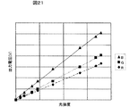
図21は検出器5に代えてカラーセンサ5’を第1の実施例における図2,図3で示す位置に取り付け、表示領域内で画像光の光強度を変化させたときに検出されるRGB毎の乱反射光の光強度特性である。図4に示した検出器5の場合の乱反射光の光強度特性と同様に、このグラフから表示領域内のR,G,B毎の光強度とその周辺に現れる乱反射光に相関関係があることが導かれる。 FIG. 21 shows the RGB detected when the color sensor 5 ′ is attached in place of the detector 5 at the position shown in FIGS. 2 and 3 in the first embodiment and the light intensity of the image light is changed in the display area. It is the light intensity characteristic of every irregularly reflected light. Similar to the light intensity characteristics of the irregularly reflected light in the case of the detector 5 shown in FIG. 4, the light intensity for each of R, G, and B in the display area and the irregularly reflected light appearing in the vicinity thereof are correlated from this graph. Is guided.
本実施例では、R,G,B毎に光強度を検出するので、表示パターンPijとしては、セルHiVjのみを白表示からR,GまたはB色表示に代えた表示パターンPijr,Pijg,Pijbを用いる。そして、これらの表示パターンは予めメモリ10に格納されている。
In this embodiment, R, G, and detects the light intensity for each B, shown as a pattern P ij, cell H i V j R only from white display, G or display pattern P was changed to B-color display ijr , P ijg, P ijb are used. These display patterns are stored in the
リファレンスデータ取得は、第1の実施例と同様に、図6で示したリファレンスデータ取得手順のフローチャートに従い、各色の表示パターンを表示させ、乱反射光の光強度をカラーセンサ5’によりR,G,B毎に取得し、取得したリファレンスデータRijr(R00rからR77r),Rijg(R00gからR77g),Rijb(R00bからR77b)をメモリ10に第1の実施例と同様に格納する。
As in the first embodiment, the reference data acquisition is performed by displaying the display pattern of each color according to the flowchart of the reference data acquisition procedure shown in FIG. 6, and the light intensity of the irregularly reflected light is R, G, and R by the color sensor 5 ′. The reference data R ijr (R 00r to R 77r ), R ijg (R 00g to R 77g ), and R ijb (R 00b to R 77b ) acquired for each B are stored in the
次の経時変化後の調整では、図7の調整手順のフローチャートに従い、セルHiVj(i,j:0〜7)において、メモリ10から読み出した各色の表示パターンを表示させ、乱反射光の光強度を検出し、検出したセンサ出力Aijr(A00rからA77r),Aijg(A00gからA77g),Aijb(A00bからA77b)を基に変化量αijr,αijg,αijbを算出し、出力電圧レベル調整回路12においてαijr,αijg,αijbがそれぞれ1.0になるまで表示デバイスの制御電圧を調整する。変化量αijr,αijg,αijbそれぞれが1.0になったら、次のセルについて同様な処理を行い、次々に64個の全てのセルHiVj(i,j:0〜7)について調整を行う。
In the next adjustment after the change with time, the display patterns of the respective colors read from the
以上により光学部品の経時変化による光強度の変化を表示パターン毎に、かつR,G,Bの色信号ごとに変化量が0になるまで表示デバイスの制御電圧を調整することによって、経時変化による映像の色バランス変化を低減することが可能である。 As described above, the change in the light intensity due to the change with time of the optical component is caused by the change with time by adjusting the control voltage of the display device until the change amount becomes 0 for each display pattern and for each color signal of R, G, B. It is possible to reduce the color balance change of the video.
以上述べた実施例(第1〜第6)では、表示デバイスとして映像信号電圧により透過率を変えて光学像を形成する透過型液晶パネルを用いたが、これに限定されるものではなく、映像信号電圧により反射率を変えて光学像を形成する反射型液晶パネルを用いることができる。勿論、映像信号電圧により透過率あるいは反射率を変えて光学像を形成する表示デバイスであれば、本発明を好適に適用できる。 In the above-described embodiments (first to sixth), the transmissive liquid crystal panel that changes the transmittance according to the video signal voltage to form an optical image is used as the display device, but the present invention is not limited to this. A reflective liquid crystal panel that forms an optical image by changing the reflectance according to the signal voltage can be used. Of course, the present invention can be suitably applied to any display device that forms an optical image by changing the transmittance or reflectance according to the video signal voltage.
また、オン反射角度とオフ反射角度の2つの反射角度を有し、その反射角度を時間に応じて切り換えて光学像を形成する微小ミラーで構成された表示デバイスにも適用できるのはいうまでもない。 Moreover, it is needless to say that the present invention can also be applied to a display device having two reflection angles, an on-reflection angle and an off-reflection angle, and switching the reflection angle according to time to form an optical image. Absent.
1…投射型表示装置、2…光学部、3…信号処理部、5…検出器、6…映像信号、7…映像信号処理回路、8…アンプ、9…A/D変換器、10…メモリ、11…マイコン、12…出力電圧レベル調整回路、13…表示デバイス駆動回路、14…フレームメモリ、15…投射レンズ、16…画像光、17…乱反射光、20…光源、21…第1レンズアレイ、22…第2レンズアレイ、23…偏光ビームスプリッター、24…合焦レンズ、25…ダイクロイックミラー、26…反射ミラー、27…コンデンサレンズ、28…入射側偏光板、29…表示デバイス、30…出射側偏光板、31…ダイクロイックミラー、32…コンデンサレンズ、33…入射側偏光板、34…表示デバイス、35…出射側偏光板、36…リレーレンズ、37…反射ミラー、38…リレーレンズ、39…反射ミラー、40…リレーレンズ、41…入射側偏光板、42…表示デバイス、43…出射側偏光板、44…合成プリズム、45…スクリーン、50…白表示部分、51…黒表示部分、52…セル、60…白表示部分、61…黒表示部分、62…セル、70…制御線。
DESCRIPTION OF
Claims (13)
光源と、該光源からの光を、駆動電圧に応じて変調して光学像を形成する表示デバイスと、該表示デバイス上の光学像を拡大投影する投射レンズと、該投射レンズからの光を検出する検出器と、該検出器の検出結果に応じて前記駆動電圧を制御する制御回路とを備え、
前記検出器は、投射レンズから出射される光束の外縁近傍に配置されることを特徴とする投射型表示装置。 In the projection display device,
A light source, a display device that modulates light from the light source according to a driving voltage to form an optical image, a projection lens that magnifies and projects the optical image on the display device, and light from the projection lens is detected And a control circuit that controls the drive voltage according to the detection result of the detector,
The projection display device, wherein the detector is arranged in the vicinity of an outer edge of a light beam emitted from a projection lens.
光源と、該光源からの光を、駆動電圧に応じて変調して光学像を形成する表示デバイスと、該表示デバイス上の光学像を拡大投影する投射レンズと、該投射レンズからの光が投影されるスクリーンと、該投射レンズからの光を検出する検出器と、該検出器の検出結果に応じて前記駆動電圧を制御する制御回路とを備え、
前記検出器は、投射レンズから出射される光のうち前記スクリーンの有効領域外に到達する光を検出することを特徴とする投射型表示装置。 In the projection display device,
A light source, a display device that modulates light from the light source according to a driving voltage to form an optical image, a projection lens that magnifies and projects the optical image on the display device, and light from the projection lens projects A screen to be detected, a detector for detecting light from the projection lens, and a control circuit for controlling the driving voltage in accordance with a detection result of the detector,
The said detector detects the light which reaches | attains the effective area | region of the said screen among the lights radiate | emitted from a projection lens, The projection type display apparatus characterized by the above-mentioned.
光源と、該光源からの光を、駆動電圧に応じて変調して光学像を形成する表示デバイスと、該表示デバイス上の光学像を拡大投影する投射レンズと、該投射レンズからの光を検出する検出器と、該検出器の検出結果に応じて前記駆動電圧を制御する制御回路とを備え、
前記検出器は、投射レンズから出射される乱反射光を検出することを特徴とする投射型表示装置。 In the projection display device,
A light source, a display device that modulates light from the light source according to a driving voltage to form an optical image, a projection lens that magnifies and projects the optical image on the display device, and light from the projection lens is detected And a control circuit that controls the drive voltage according to the detection result of the detector,
The said detector detects the irregular reflection light radiate | emitted from a projection lens, The projection type display apparatus characterized by the above-mentioned.
光源と、該光源からの光を、駆動電圧に応じて変調して光学像を形成する表示デバイスと、該表示デバイス上の光学像を拡大投影する投射レンズと、該投射レンズからの光が投影されるスクリーンと、該投射レンズからの光を検出する検出器と、該検出器の検出結果に応じて光源に印加される電圧を制御する制御回路とを備え、
前記検出器は、投射レンズから出射される乱反射光を検出することを特徴とする投射型表示装置。 In the projection display device,
A light source, a display device that modulates light from the light source according to a driving voltage to form an optical image, a projection lens that magnifies and projects the optical image on the display device, and light from the projection lens projects A screen to be detected, a detector for detecting light from the projection lens, and a control circuit for controlling a voltage applied to the light source according to a detection result of the detector,
The said detector detects the irregular reflection light radiate | emitted from a projection lens, The projection type display apparatus characterized by the above-mentioned.
前記複数の投射型表示装置の各々は、光源と、該光源からの光を、駆動電圧に応じて変調して光学像を形成する表示デバイスと、該表示デバイス上の光学像を拡大投影する投射レンズと、該投射レンズからの光が投影されるスクリーンと、該投射レンズからの光を検出する検出器と、該検出器の検出結果に応じて前記複数の投射型表示装置間の輝度差を補正するように制御する制御回路とを備え、
前記検出器は、投射レンズから出射される乱反射光を検出することを特徴とするマルチスクリーン表示装置。 In a multi-screen display device combining a plurality of projection display devices,
Each of the plurality of projection display devices includes a light source, a display device that modulates light from the light source according to a driving voltage to form an optical image, and a projection that magnifies and projects the optical image on the display device A lens, a screen on which light from the projection lens is projected, a detector for detecting light from the projection lens, and a luminance difference between the plurality of projection display devices according to a detection result of the detector. A control circuit that controls to correct,
The multi-screen display device, wherein the detector detects irregularly reflected light emitted from a projection lens.
12. The multi-screen display device according to claim 11, wherein the control circuit is detected by the detector when the voltage applied to the light source or the driving voltage of the display device cannot be controlled at a certain rate of change. A multi-screen display device that performs voltage control in accordance with a minimum value of light intensity data.
Priority Applications (3)
| Application Number | Priority Date | Filing Date | Title |
|---|---|---|---|
| JP2005012232A JP4736436B2 (en) | 2005-01-20 | 2005-01-20 | Projection type display device and multi-screen display device |
| US11/312,763 US7543944B2 (en) | 2005-01-20 | 2005-12-21 | Projection-type display apparatus and multiscreen display apparatus |
| CNB2006100012061A CN100520564C (en) | 2005-01-20 | 2006-01-10 | Projection-type display apparatus and multiscreen display apparatus |
Applications Claiming Priority (1)
| Application Number | Priority Date | Filing Date | Title |
|---|---|---|---|
| JP2005012232A JP4736436B2 (en) | 2005-01-20 | 2005-01-20 | Projection type display device and multi-screen display device |
Publications (2)
| Publication Number | Publication Date |
|---|---|
| JP2006201416A true JP2006201416A (en) | 2006-08-03 |
| JP4736436B2 JP4736436B2 (en) | 2011-07-27 |
Family
ID=36683430
Family Applications (1)
| Application Number | Title | Priority Date | Filing Date |
|---|---|---|---|
| JP2005012232A Expired - Fee Related JP4736436B2 (en) | 2005-01-20 | 2005-01-20 | Projection type display device and multi-screen display device |
Country Status (3)
| Country | Link |
|---|---|
| US (1) | US7543944B2 (en) |
| JP (1) | JP4736436B2 (en) |
| CN (1) | CN100520564C (en) |
Cited By (2)
| Publication number | Priority date | Publication date | Assignee | Title |
|---|---|---|---|---|
| CN101995749A (en) * | 2009-08-21 | 2011-03-30 | 卡西欧计算机株式会社 | Light source device, projection device and projection method |
| JP2021092757A (en) * | 2019-11-28 | 2021-06-17 | 株式会社リコー | Image projection device |
Families Citing this family (8)
| Publication number | Priority date | Publication date | Assignee | Title |
|---|---|---|---|---|
| US20080024674A1 (en) * | 2006-02-06 | 2008-01-31 | Toshiba America Consumer Products, Llc. | Brightness control system and method |
| US9110495B2 (en) * | 2010-02-03 | 2015-08-18 | Microsoft Technology Licensing, Llc | Combined surface user interface |
| CN105491359B (en) * | 2014-10-13 | 2018-07-06 | 联想(北京)有限公司 | Projection device, optical projection system and projecting method |
| CN105991980B (en) * | 2015-02-06 | 2019-05-03 | 深圳光峰科技股份有限公司 | Projection system and control method thereof |
| JP6699189B2 (en) * | 2016-01-19 | 2020-05-27 | セイコーエプソン株式会社 | Projector and projector control method |
| CN107728413B (en) * | 2016-08-12 | 2019-07-16 | 深圳光峰科技股份有限公司 | Optical projection system and brightness adjusting method applied to optical projection system |
| KR102478607B1 (en) * | 2018-03-27 | 2022-12-16 | 삼성전자주식회사 | Electronic appratus and operating method for the same |
| DE102019212673A1 (en) * | 2019-07-22 | 2021-01-28 | OSRAM CONTINENTAL GmbH | OPTICAL ARRANGEMENT AND PROCEDURE |
Citations (4)
| Publication number | Priority date | Publication date | Assignee | Title |
|---|---|---|---|---|
| JPH06217242A (en) * | 1993-01-14 | 1994-08-05 | Matsushita Electric Ind Co Ltd | Image display device |
| JPH07284120A (en) * | 1994-04-07 | 1995-10-27 | Hitachi Ltd | Multi display device |
| JP2000148075A (en) * | 1998-11-10 | 2000-05-26 | Nec Corp | System and method for correcting color, and multi- projector system |
| JP2003228046A (en) * | 2001-12-15 | 2003-08-15 | Samsung Electronics Co Ltd | Apparatus and method for controlling driving voltage of image display element |
Family Cites Families (18)
| Publication number | Priority date | Publication date | Assignee | Title |
|---|---|---|---|---|
| JPH0273241A (en) | 1988-09-08 | 1990-03-13 | Hitachi Ltd | Screen brightness control method and device for projection display |
| JPH08278512A (en) * | 1995-04-06 | 1996-10-22 | Sharp Corp | Liquid crystal display |
| JP2001117164A (en) | 1999-10-14 | 2001-04-27 | Nec Viewtechnology Ltd | Automatic luminance adjusting device and method for light source for projector |
| US20030067587A1 (en) * | 2000-06-09 | 2003-04-10 | Masami Yamasaki | Multi-projection image display device |
| US6788469B2 (en) * | 2000-12-30 | 2004-09-07 | Texas Instruments Incorporated | Automated lamp focus |
| CN100452852C (en) * | 2002-01-02 | 2009-01-14 | 皇家飞利浦电子股份有限公司 | Image projector and method of operating the same |
| EP1485904B1 (en) * | 2002-03-13 | 2012-08-29 | Dolby Laboratories Licensing Corporation | High dynamic range display devices |
| JP2003324670A (en) | 2002-05-01 | 2003-11-14 | Canon Inc | Projection type video display |
| US20040021831A1 (en) * | 2002-07-31 | 2004-02-05 | Canon Kabushiki Kaisha, Tokyo, Japan | Projection type image display apparatus and image display system |
| JP2004062109A (en) | 2002-07-31 | 2004-02-26 | Canon Inc | Projection display device |
| DE10248376A1 (en) * | 2002-10-17 | 2004-04-29 | Philips Intellectual Property & Standards Gmbh | projection system |
| JP2004157348A (en) * | 2002-11-07 | 2004-06-03 | Chinontec Kk | Projection lens device and projector device |
| JP4245563B2 (en) * | 2002-12-26 | 2009-03-25 | 三洋電機株式会社 | Projection display device |
| JP4086664B2 (en) * | 2003-01-07 | 2008-05-14 | 三菱電機株式会社 | Illumination optical system structure and projection display device |
| JP2004228948A (en) | 2003-01-23 | 2004-08-12 | Seiko Epson Corp | Image processing system, projector, program, information storage medium, and image processing method |
| US7018050B2 (en) * | 2003-09-08 | 2006-03-28 | Hewlett-Packard Development Company, L.P. | System and method for correcting luminance non-uniformity of obliquely projected images |
| JP4426281B2 (en) * | 2003-12-25 | 2010-03-03 | 船井電機株式会社 | Projector device |
| US7278745B2 (en) * | 2004-12-21 | 2007-10-09 | Infocus Corporation | Method and apparatus for adjusting relative disposition of projection optics based on operating conditions |
-
2005
- 2005-01-20 JP JP2005012232A patent/JP4736436B2/en not_active Expired - Fee Related
- 2005-12-21 US US11/312,763 patent/US7543944B2/en active Active
-
2006
- 2006-01-10 CN CNB2006100012061A patent/CN100520564C/en not_active Expired - Fee Related
Patent Citations (4)
| Publication number | Priority date | Publication date | Assignee | Title |
|---|---|---|---|---|
| JPH06217242A (en) * | 1993-01-14 | 1994-08-05 | Matsushita Electric Ind Co Ltd | Image display device |
| JPH07284120A (en) * | 1994-04-07 | 1995-10-27 | Hitachi Ltd | Multi display device |
| JP2000148075A (en) * | 1998-11-10 | 2000-05-26 | Nec Corp | System and method for correcting color, and multi- projector system |
| JP2003228046A (en) * | 2001-12-15 | 2003-08-15 | Samsung Electronics Co Ltd | Apparatus and method for controlling driving voltage of image display element |
Cited By (4)
| Publication number | Priority date | Publication date | Assignee | Title |
|---|---|---|---|---|
| CN101995749A (en) * | 2009-08-21 | 2011-03-30 | 卡西欧计算机株式会社 | Light source device, projection device and projection method |
| CN101995749B (en) * | 2009-08-21 | 2012-08-08 | 卡西欧计算机株式会社 | Light source device, projection device and projection method |
| JP2021092757A (en) * | 2019-11-28 | 2021-06-17 | 株式会社リコー | Image projection device |
| JP7494635B2 (en) | 2019-11-28 | 2024-06-04 | 株式会社リコー | Image Projection Device |
Also Published As
| Publication number | Publication date |
|---|---|
| US7543944B2 (en) | 2009-06-09 |
| US20060158516A1 (en) | 2006-07-20 |
| JP4736436B2 (en) | 2011-07-27 |
| CN100520564C (en) | 2009-07-29 |
| CN1808265A (en) | 2006-07-26 |
Similar Documents
| Publication | Publication Date | Title |
|---|---|---|
| CN100507704C (en) | Projection display device | |
| US7605828B2 (en) | Method and system for reducing gray scale discontinuities in contrast enhancing screens affected by ambient light | |
| US8011789B2 (en) | Rear projection display | |
| JP2006319950A (en) | Video display device | |
| JP5071442B2 (en) | Liquid crystal display device, control method, and electronic apparatus | |
| US7384157B2 (en) | Projection type video display | |
| JP4736436B2 (en) | Projection type display device and multi-screen display device | |
| JP3353320B2 (en) | Gradation correction device and laser display device | |
| CN104749864B (en) | Image display device and its control method | |
| US6771233B1 (en) | Projection display device using two liquid crystal display panels | |
| JP3299058B2 (en) | LCD projector | |
| JPH0764522A (en) | Multi-display device automatic adjustment system | |
| WO2017017758A1 (en) | Projector device and method for correcting color in projector device | |
| JP2009231853A (en) | Image adjusting device, image display system, and image adjusting method | |
| JP2005150922A (en) | Apparatus and method for adjusting display state of projector | |
| JP4909665B2 (en) | Liquid crystal display device and common voltage adjustment method | |
| JP4595961B2 (en) | Projection display | |
| JP2008089836A (en) | projector | |
| JPH06217336A (en) | Automatic adjustment system for multi display device | |
| US7253796B2 (en) | Circuit for and method of driving liquid crystal panel of liquid crystal projector | |
| JP6398162B2 (en) | Image processing circuit, electro-optical device and electronic apparatus | |
| JP4683022B2 (en) | Projection display | |
| JP2009294265A (en) | Image display device | |
| JP2005227577A (en) | Liquid crystal projector | |
| KR20000028261A (en) | Method for controlling automatically convergence ofprojection television |
Legal Events
| Date | Code | Title | Description |
|---|---|---|---|
| RD04 | Notification of resignation of power of attorney |
Free format text: JAPANESE INTERMEDIATE CODE: A7424 Effective date: 20060425 |
|
| A621 | Written request for application examination |
Free format text: JAPANESE INTERMEDIATE CODE: A621 Effective date: 20070314 |
|
| A977 | Report on retrieval |
Free format text: JAPANESE INTERMEDIATE CODE: A971007 Effective date: 20100415 |
|
| A131 | Notification of reasons for refusal |
Free format text: JAPANESE INTERMEDIATE CODE: A131 Effective date: 20100713 |
|
| A521 | Request for written amendment filed |
Free format text: JAPANESE INTERMEDIATE CODE: A523 Effective date: 20100909 |
|
| A131 | Notification of reasons for refusal |
Free format text: JAPANESE INTERMEDIATE CODE: A131 Effective date: 20101124 |
|
| A521 | Request for written amendment filed |
Free format text: JAPANESE INTERMEDIATE CODE: A523 Effective date: 20110119 |
|
| TRDD | Decision of grant or rejection written | ||
| A01 | Written decision to grant a patent or to grant a registration (utility model) |
Free format text: JAPANESE INTERMEDIATE CODE: A01 Effective date: 20110405 |
|
| A61 | First payment of annual fees (during grant procedure) |
Free format text: JAPANESE INTERMEDIATE CODE: A61 Effective date: 20110418 |
|
| R151 | Written notification of patent or utility model registration |
Ref document number: 4736436 Country of ref document: JP Free format text: JAPANESE INTERMEDIATE CODE: R151 |
|
| FPAY | Renewal fee payment (event date is renewal date of database) |
Free format text: PAYMENT UNTIL: 20140513 Year of fee payment: 3 |
|
| S111 | Request for change of ownership or part of ownership |
Free format text: JAPANESE INTERMEDIATE CODE: R313111 |
|
| R350 | Written notification of registration of transfer |
Free format text: JAPANESE INTERMEDIATE CODE: R350 |
|
| S111 | Request for change of ownership or part of ownership |
Free format text: JAPANESE INTERMEDIATE CODE: R313111 |
|
| R350 | Written notification of registration of transfer |
Free format text: JAPANESE INTERMEDIATE CODE: R350 |
|
| R250 | Receipt of annual fees |
Free format text: JAPANESE INTERMEDIATE CODE: R250 |
|
| R250 | Receipt of annual fees |
Free format text: JAPANESE INTERMEDIATE CODE: R250 |
|
| R250 | Receipt of annual fees |
Free format text: JAPANESE INTERMEDIATE CODE: R250 |
|
| R250 | Receipt of annual fees |
Free format text: JAPANESE INTERMEDIATE CODE: R250 |
|
| S111 | Request for change of ownership or part of ownership |
Free format text: JAPANESE INTERMEDIATE CODE: R313111 |
|
| R350 | Written notification of registration of transfer |
Free format text: JAPANESE INTERMEDIATE CODE: R350 |
|
| R250 | Receipt of annual fees |
Free format text: JAPANESE INTERMEDIATE CODE: R250 |
|
| LAPS | Cancellation because of no payment of annual fees |