JP2006166399A - EMC test antenna device, test signal generator, and transmitter - Google Patents
EMC test antenna device, test signal generator, and transmitter Download PDFInfo
- Publication number
- JP2006166399A JP2006166399A JP2005104826A JP2005104826A JP2006166399A JP 2006166399 A JP2006166399 A JP 2006166399A JP 2005104826 A JP2005104826 A JP 2005104826A JP 2005104826 A JP2005104826 A JP 2005104826A JP 2006166399 A JP2006166399 A JP 2006166399A
- Authority
- JP
- Japan
- Prior art keywords
- test
- lens
- horn antenna
- radiation characteristic
- emc
- Prior art date
- Legal status (The legal status is an assumption and is not a legal conclusion. Google has not performed a legal analysis and makes no representation as to the accuracy of the status listed.)
- Pending
Links
Images
Landscapes
- Testing Electric Properties And Detecting Electric Faults (AREA)
- Aerials With Secondary Devices (AREA)
- Waveguide Aerials (AREA)
Abstract
【課題】 EMC試験(特にイミュニティ試験)に用いられる送信装置を、コストアップを招くことなく、試験対象物に対して試験用電波を適正に照射できるようにする。
【解決手段】 送信装置は、ホーンアンテナ20と、その放射方向等を補正する誘電体レンズ30とを備える。誘電体レンズ30は、レンズ部32と、鍔部34と、突起部36とから構成され、鍔部34をホーンアンテナ20の開口端に当接し、突起部36をホーンアンテナ20に溶接されたL字金具22にビス止めすることにより、ホーンアンテナ20の開口端に直接固定される。この結果、ホーンアンテナ20からの送信電波は、誘電体レンズ30に損失なく入射し、しかも、誘電体レンズ30を通過することなく試験対象物側に放射されることはない。従って、ホーンアンテナ20のゲインや誘電体レンズ30の形状を大きくする必要がなく、送信装置を低コストで実現できる。
【選択図】 図2
PROBLEM TO BE SOLVED: To appropriately irradiate a test object with a test radio wave without causing a cost increase in a transmission device used for an EMC test (particularly, an immunity test).
A transmission apparatus includes a horn antenna 20 and a dielectric lens 30 that corrects a radiation direction and the like of the horn antenna. The dielectric lens 30 includes a lens portion 32, a flange portion 34, and a projection portion 36. The dielectric lens 30 is in contact with the opening end of the horn antenna 20 and the projection portion 36 is welded to the horn antenna 20. By fixing with screws to the bracket 22, the horn antenna 20 is directly fixed to the open end. As a result, the transmission radio wave from the horn antenna 20 is incident on the dielectric lens 30 without loss, and is not radiated to the test object side without passing through the dielectric lens 30. Therefore, it is not necessary to increase the gain of the horn antenna 20 or the shape of the dielectric lens 30, and the transmission device can be realized at low cost.
[Selection] Figure 2
Description
本発明は、EMC試験、特に、妨害波による試験対象物の耐性を測定するイミュニティ試験、を行うのに好適なEMC試験用アンテナ装置、試験信号発生装置及び送信装置に関する。 The present invention relates to an EMC test antenna device, a test signal generation device, and a transmission device suitable for performing an EMC test, in particular, an immunity test for measuring resistance of a test object due to an interference wave.
従来より、電子装置や電子部品の電磁環境適合性(EMC:Electro Magnetic Compatibility)を評価するEMC試験として、試験の対象物(電子装置や電子部品)自身から放射される妨害波の大きさを測定するエミッション試験と、外部からの妨害波を受けた際の機器の耐性を測定するイミュニティ試験とが知られている。 Conventionally, as an EMC test for evaluating the electromagnetic compatibility (EMC) of electronic devices and electronic components, the magnitude of the interference wave emitted from the test object (electronic device or electronic component) itself has been measured. Emission tests to be performed and immunity tests to measure the resistance of devices when subjected to external interference are known.
また、このイミュニティ試験では、試験対象物に対し、妨害波として、所定周波数帯(例えば、放射電磁界試験では、数十MHz〜数GHz)の試験用電波を照射することになるが、このとき試験対象物に照射する試験用電波の強度や照射範囲は、国際電気標準会議(IEC)等の国際規格で規定されている。 In this immunity test, the test object is irradiated with test radio waves in a predetermined frequency band (for example, several tens of MHz to several GHz in the radiated electromagnetic field test) as an interference wave. The intensity and irradiation range of the test radio wave applied to the test object are defined by international standards such as the International Electrotechnical Commission (IEC).
このため、イミュニティ試験を行う際に用いられる妨害波(換言すれば試験用電波)の送信装置としては、従来より、試験対象物に対して試験用電波を適正に照射できるようにするために、試験用電波を放射するアンテナ(ホーンアンテナ)と試験対象物との間に誘電体レンズを配置し、この誘電体レンズを用いて、試験対象物に対する試験用電波の照射範囲や照射レベルを補正することが提案されている(例えば、特許文献1等参照)。 For this reason, as a transmission device for disturbing waves (in other words, test radio waves) used when performing an immunity test, in order to be able to properly radiate test radio waves to a test object, A dielectric lens is placed between the antenna that radiates the test radio wave (horn antenna) and the test object, and the irradiation range and level of the test radio wave on the test object are corrected using this dielectric lens. (For example, refer to Patent Document 1).
そして、この提案の装置によれば、誘電体レンズの曲率や誘電率を適宜設定することにより、試験対象物に対する試験用電波の照射範囲が適正範囲になるように調整したり、その照射範囲全域で試験用電波の位相を一致させる、といったことができるようになる。
しかし、上記提案の送信装置において、誘電体レンズは、ホーンアンテナに対して離れた位置に配置するように構成されているため、ホーンアンテナから放射された試験用電波は、ホーンアンテナと誘電体レンズとの間の空間で生じる伝送損失、及び、誘電体レンズ表面での反射等によって、減衰されてしまい、試験対象物での試験用電波の強度を適正レベルに確保するには、その減衰量だけホーンアンテナのゲイン(利得)を大きくしなければならず、ホーンアンテナの大型化、延いては装置のコストアップを招くという問題があった。 However, in the proposed transmission device, the dielectric lens is configured to be arranged at a position distant from the horn antenna. Therefore, the test radio wave radiated from the horn antenna is transmitted between the horn antenna and the dielectric lens. In order to ensure that the strength of the test radio wave at the test object is at an appropriate level, it is attenuated by the transmission loss that occurs in the space between it and the reflection on the surface of the dielectric lens. There has been a problem that the gain of the horn antenna has to be increased, leading to an increase in the size of the horn antenna and an increase in the cost of the device.
また、ホーンアンテナからは、その開口面から広がるように試験用電波が放射されることから、誘電体レンズをホーンアンテナから離れた位置に配置すると、ホーンアンテナから放射された試験用電波の一部は、誘電体レンズを通ることなく試験対象物方向に放射されてしまい、この電波がEMC試験(イミュニティ試験)に悪影響を与えることも考えられる。なお、この問題を防止するには、ホーンアンテナから放射された電波が全て誘電体レンズに届くように、誘電体レンズの径を大きくすればよいが、誘電体レンズの径を大きくすると、装置のコストアップを招くことになる。 In addition, since the test radio wave is radiated from the horn antenna so as to spread from the opening surface, if the dielectric lens is disposed at a position away from the horn antenna, a part of the test radio wave radiated from the horn antenna is obtained. May be radiated in the direction of the test object without passing through the dielectric lens, and this radio wave may adversely affect the EMC test (immunity test). In order to prevent this problem, the diameter of the dielectric lens may be increased so that all the radio waves radiated from the horn antenna reach the dielectric lens. However, if the diameter of the dielectric lens is increased, This will increase the cost.
本発明は、こうした問題に鑑みなされたもので、EMC試験、特に、妨害波による試験対象物の耐性を測定するイミュニティ試験を行うに当たって、妨害波としての試験用電波を送信するのに用いられる送信装置(ホーンアンテナや誘電体レンズ等)のコストアップを招くことなく、試験対象物に対して試験用電波を適正に照射できるようにすることを目的とする。 The present invention has been made in view of these problems, and is used to transmit a test radio wave as an interference wave in performing an EMC test, particularly an immunity test for measuring the resistance of a test object due to the interference wave. It is an object of the present invention to appropriately irradiate a test object with a test radio wave without increasing the cost of a device (horn antenna, dielectric lens, etc.).
かかる目的を達成するためになされた請求項1に記載の発明は、試験対象物のEMC試験を行うのに用いられるEMC試験用アンテナ装置であって、試験対象物に向けて試験用電波を放射するホーンアンテナと、このホーンアンテナからの試験用電波の放射特性を補正する放射特性補正レンズとを備え、放射特性補正レンズをホーンアンテナの開口端に配置してなることを特徴とする。
The invention according to
このように、本発明のEMC試験用アンテナ装置においては、試験用電波を放射するホーンアンテナの開口端に、その試験用電波の放射特性を補正するための放射特性補正レンズが配置されることから、ホーンアンテナからの送信電波が放射特性補正レンズに損失なく入射することになり、上述した従来装置のように、ホーンアンテナから放射特性補正レンズに至る試験用電波の伝送経路で生じる伝送損失を補うために、ホーンアンテナのゲインを大きくする必要はない。 As described above, in the EMC test antenna device of the present invention, the radiation characteristic correction lens for correcting the radiation characteristic of the test radio wave is disposed at the opening end of the horn antenna that radiates the test radio wave. The transmission radio wave from the horn antenna enters the radiation characteristic correction lens without loss, and compensates for the transmission loss generated in the transmission path of the test radio wave from the horn antenna to the radiation characteristic correction lens as in the above-described conventional device. Therefore, it is not necessary to increase the gain of the horn antenna.
また、放射特性補正レンズは、ホーンアンテナの開口端に配置されることから、ホーンアンテナからの送信電波は必ず放射特性補正レンズを通って外部に放射されることになり、上述した従来装置のように、ホーンアンテナからの送信電波の一部が放射特性補正レンズを通ることなく試験対象物方向に放射されてしまい、その電波がEMC試験(イミュニティ試験)に悪影響を与えることはない。 In addition, since the radiation characteristic correction lens is arranged at the opening end of the horn antenna, the transmission radio wave from the horn antenna is always radiated to the outside through the radiation characteristic correction lens. In addition, a part of the transmission radio wave from the horn antenna is radiated in the direction of the test object without passing through the radiation characteristic correcting lens, and the radio wave does not adversely affect the EMC test (immunity test).
また、放射特性補正レンズは、ホーンアンテナの開口端と略同じ径にすればよく、上述した従来装置のように、レンズの径を、ホーンアンテナ20の開口端に比べて著しく大きくする必要はない。
In addition, the radiation characteristic correction lens may have substantially the same diameter as the opening end of the horn antenna, and the diameter of the lens does not need to be significantly larger than that of the opening end of the
よって、本発明のEMC試験用アンテナ装置によれば、ホーンアンテナや放射特性補正レンズを大型化することなく、試験対象物に対して試験用電波を適正に照射できるようになり、EMC試験(特に妨害波による試験対象物の耐性を測定するイミュニティ試験)を行うのに適したアンテナ装置を、低コストで実現できることになる。 Therefore, according to the EMC test antenna device of the present invention, the test object can be appropriately irradiated with the test radio wave without increasing the size of the horn antenna or the radiation characteristic correcting lens. An antenna device suitable for performing an immunity test for measuring the resistance of a test object due to an interference wave can be realized at low cost.
ここで、放射特性補正レンズは、ホーンアンテナ単体での電波の放射特性を試験に適した放射特性に補正するものであることから、ホーンアンテナ単体での電波の放射特性に応じて、レンズの種類や形状を設定すればよいが、レンズの種類としては、請求項3に記載のように、上述した公報に開示されているような誘電体レンズであってもよく、或いは、請求項2に記載のように、複数の金属板(メタルプレート)を所定の間隔を開けて平行に配置したメタルプレートレンズであってもよい。 Here, the radiation characteristic correction lens corrects the radiation characteristic of the horn antenna alone to the radiation characteristic suitable for the test. The shape of the lens may be a dielectric lens as disclosed in the above-mentioned publication as described in claim 3, or according to claim 2. As described above, a metal plate lens in which a plurality of metal plates (metal plates) are arranged in parallel at predetermined intervals may be used.
また、請求項3に記載のように放射特性補正レンズを誘電体レンズにて構成する場合には、請求項4又は請求項5に記載のように、一般的な凸レンズ若しくは凹レンズにすればよい。 Further, when the radiation characteristic correcting lens is configured by a dielectric lens as described in claim 3, it may be a general convex lens or concave lens as described in claim 4 or claim 5.
但し、この場合、レンズの表・裏面が連続する曲面となるので、レンズの厚みが大きくなり過ぎ(換言すれば重くなり過ぎ)、ホーンアンテナの開口端に配置し難くなることも考えられる。 However, in this case, since the front and back surfaces of the lens are continuous curved surfaces, it is conceivable that the thickness of the lens becomes too large (in other words, too heavy), making it difficult to place the lens at the opening end of the horn antenna.
そこで、このような場合には、請求項6に記載のように、放射特性補正レンズ(つまり誘電体レンズ)を、フレネルレンズで構成するようにしてもよい。そして、このように誘電体レンズをフレネルレンズにて構成すれば、レンズ全体の厚みを小さくして、誘電体レンズの軽量化を図ることができる。 Therefore, in such a case, as described in claim 6, the radiation characteristic correcting lens (that is, the dielectric lens) may be constituted by a Fresnel lens. If the dielectric lens is constituted by a Fresnel lens in this way, the thickness of the entire lens can be reduced, and the weight of the dielectric lens can be reduced.
また、本発明において、放射特性補正レンズは、試験対象物に対する試験用電波の照射特性が予め設定された試験用の規格に沿ったものとなるように、ホーンアンテナからの電波の放射特性を補正するためのものであるが、このためには、放射特性補正レンズの電波の透過特性が、試験に使用するホーンアンテナや試験対象物の仕様に応じた最適な特性となるように調整する必要がある。 In the present invention, the radiation characteristic correcting lens corrects the radiation characteristic of the radio wave from the horn antenna so that the irradiation characteristic of the test radio wave to the test object is in accordance with a preset test standard. However, for this purpose, it is necessary to adjust the radio wave transmission characteristics of the radiation correction lens so that it is optimal for the specifications of the horn antenna and test object used in the test. is there.
そして、放射特性補正レンズをメタルプレートレンズにて構成した際には、レンズを構成している各メタルプレートの形状を適宜変更すればよいが、放射特性補正レンズとして誘電体レンズを利用する場合には、レンズの誘電率や厚み等を調整する必要があることから、その調整が難しいという問題がある。 When the radiation characteristic correction lens is configured with a metal plate lens, the shape of each metal plate constituting the lens may be changed as appropriate, but when a dielectric lens is used as the radiation characteristic correction lens. However, since it is necessary to adjust the dielectric constant, thickness, etc. of the lens, there is a problem that the adjustment is difficult.
そこで、放射特性補正レンズとして誘電体レンズを利用し、その調整作業を効率よく行えるようにするには、請求項7に記載のように、放射特性補正レンズ(つまり誘電体レンズ)を、レンズの表面から裏面にかけて複数に分割することで、その分割したレンズ部材毎に特性を調整できるようにし、この放射特性補正レンズ(つまり誘電体レンズ)をホーンアンテナの開口端に配置する際には、その分割された複数のレンズ部材を接合した状態でホーンアンテナの開口端に配置するようにするとよい。 Therefore, in order to efficiently use the dielectric lens as the radiation characteristic correction lens and perform the adjustment work, the radiation characteristic correction lens (that is, the dielectric lens) is attached to the lens as described in claim 7. By dividing into multiple parts from the front surface to the back surface, the characteristics can be adjusted for each of the divided lens members, and when this radiation characteristic correction lens (that is, a dielectric lens) is disposed at the opening end of the horn antenna, A plurality of divided lens members may be joined at the opening end of the horn antenna.
なお、このように放射特性補正レンズを複数のレンズ部材にて構成した場合、各レンズ部材の接合は、接合面に接着剤を塗布することにより行うようにしてもよく、粘着テープを利用して各レンズ部材を外側から接合するようにしてもよい。 In addition, when the radiation characteristic correcting lens is configured by a plurality of lens members in this manner, the lens members may be bonded by applying an adhesive to the bonding surface, and using an adhesive tape. Each lens member may be joined from the outside.
但し、この場合、放射特性補正レンズの電波の通過特性に影響を与えることのないようにするために、接着剤や粘着テープには、レンズと略同じ誘電率を有する材料のものを用い、その厚さは、試験用電波の波長の1/4以下(より好ましくは1/16以下)にすることが望ましい。 However, in this case, in order not to affect the radio wave transmission characteristics of the radiation characteristic correction lens, the adhesive or the adhesive tape is made of a material having substantially the same dielectric constant as the lens. The thickness is desirably set to 1/4 or less (more preferably 1/16 or less) of the wavelength of the test radio wave.
一方、本発明のEMC試験用アンテナ装置では、放射特性補正レンズがホーンアンテナの開口端に配置されるが、配置後に、放射特性補正レンズとホーンアンテナとの相対位置がずれると、当該アンテナ装置からの試験用電波の放射特性が変化してしまうことから、放射特性補正レンズは、ホーンアンテナの開口端に対して、しっかりと位置決めできるようにする必要がある。 On the other hand, in the EMC test antenna device of the present invention, the radiation characteristic correction lens is disposed at the opening end of the horn antenna. If the relative position between the radiation characteristic correction lens and the horn antenna is shifted after the placement, the antenna device is separated from the antenna device. Therefore, the radiation characteristic correction lens needs to be able to be firmly positioned with respect to the opening end of the horn antenna.
そして、このためには、放射特性補正レンズが誘電体レンズである場合には、例えば、請求項8に記載のように、放射特性補正レンズのレンズ面周囲の外周部に、鍔部を設けるようにするとよい。 For this purpose, when the radiation characteristic correction lens is a dielectric lens, for example, as shown in claim 8, a flange is provided on the outer periphery of the lens surface of the radiation characteristic correction lens. It is good to.
つまり、このように、放射特性補正レンズ(誘電体レンズ)の外周部に鍔部を設けるようにすれば、放射特性補正レンズ(誘電体レンズ)をホーンアンテナの開口端に配置する際に、この鍔部をホーンアンテナの開口端に当接させることによって、ホーンアンテナの開口端に放射特性補正レンズ(誘電体レンズ)をしっかりと位置決めできるようになり、当該アンテナ装置の使用時に、放射特性補正レンズ(誘電体レンズ)とホーンアンテナとの相対位置がずれて、当該アンテナ装置からの試験用電波の放射特性が変化してしまう、といったことを防止できる。 That is, in this way, when the collar portion is provided on the outer periphery of the radiation characteristic correction lens (dielectric lens), when the radiation characteristic correction lens (dielectric lens) is disposed at the opening end of the horn antenna, By bringing the buttocks into contact with the opening end of the horn antenna, the radiation characteristic correcting lens (dielectric lens) can be firmly positioned at the opening end of the horn antenna. It is possible to prevent the relative position between the (dielectric lens) and the horn antenna from being shifted and the radiation characteristics of the test radio wave from the antenna device to change.
また、このように放射特性補正レンズ(誘電体レンズ)の外周部に鍔部を設ける場合には、更に請求項9に記載のように、この鍔部に、ホーンアンテナの開口端周囲を囲むように複数の突起部を設けるようにしてもよい。そして、このようにすれば、鍔部に設けた突起部によって、ホーンアンテナに対して放射特性補正レンズ(誘電体レンズ)をより正確に位置決めできるようになり、当該アンテナ装置の使用時に放射特性補正レンズ(誘電体レンズ)とホーンアンテナとの相対位置がずれるのをより確実に防止できる。 Further, in the case where the flange portion is provided on the outer peripheral portion of the radiation characteristic correction lens (dielectric lens) in this way, as described in claim 9, the flange portion is surrounded by the periphery of the opening end of the horn antenna. A plurality of protrusions may be provided on the surface. In this way, the projection provided on the collar allows the radiation characteristic correction lens (dielectric lens) to be more accurately positioned with respect to the horn antenna, and correction of the radiation characteristic when the antenna device is used. The relative position between the lens (dielectric lens) and the horn antenna can be prevented more reliably.
また、ホーンアンテナの開口端に放射特性補正レンズ(誘電体レンズ)を配置するには、これら各部とは別体で構成された配置用の部材を使用するようにしてもよいが、請求項9に記載のように、放射特性補正レンズ(誘電体レンズ)の外周部に設けられた鍔部に複数の突起部を設けた場合には、請求項10に記載のように、ホーンアンテナの外周面に、放射特性補正レンズ(誘電体レンズ)の鍔部に設けられた複数の突起部をホーンアンテナに接合するための複数の接合用金具を設けるようにするとよい。 Further, in order to dispose the radiation characteristic correction lens (dielectric lens) at the opening end of the horn antenna, a disposing member configured separately from these respective parts may be used. When the plurality of protrusions are provided on the flange provided on the outer peripheral portion of the radiation characteristic correction lens (dielectric lens) as described in claim 10, the outer peripheral surface of the horn antenna as described in claim 10 In addition, it is preferable to provide a plurality of joining metal fittings for joining a plurality of protrusions provided on the flange portion of the radiation characteristic correcting lens (dielectric lens) to the horn antenna.
つまりこのようにすれば、放射特性補正レンズ(誘電体レンズ)の鍔部に設けた複数の突起部を、ホーンアンテナの開口端に対する放射特性補正レンズ(誘電体レンズ)の位置決め用兼固定用の部材として利用することができるようになり、ホーンアンテナの開口端へ放射特性補正レンズ(誘電体レンズ)を配置するのに使用する配置用部材の構成を簡単にし、当該アンテナ装置のコストダウンを図ることができる。 In other words, in this way, the plurality of protrusions provided on the flange portion of the radiation characteristic correction lens (dielectric lens) are used for positioning and fixing the radiation characteristic correction lens (dielectric lens) with respect to the opening end of the horn antenna. It can be used as a member, and the arrangement of the arrangement member used to arrange the radiation characteristic correction lens (dielectric lens) at the opening end of the horn antenna is simplified, and the cost of the antenna device is reduced. be able to.
一方、放射特性補正レンズをホーンアンテナの開口端に位置決めするには、必ずしも、放射特性補正レンズを誘電体レンズにて構成して、その外周部に鍔部を設ける必要はなく、例えば、請求項11に記載のように、放射特性補正レンズを一対の挟持部材にて挟持するようにし、その一対の挟持部材の一方をホーンアンテナの内部に収納し、他方の挟持部材を、放射特性補正レンズを挟んでホーンアンテナの外側に配置し、更に、その他方の挟持部材を、固定部材を介してホーンアンテナに固定することにより、ホーンアンテナの開口端に放射特性補正レンズを配置するようにしてもよい。 On the other hand, in order to position the radiation characteristic correction lens at the opening end of the horn antenna, it is not always necessary to configure the radiation characteristic correction lens with a dielectric lens and to provide a flange on the outer periphery thereof. 11, the radiation characteristic correction lens is sandwiched between a pair of sandwiching members, one of the pair of sandwiching members is housed inside the horn antenna, and the other sandwiching member is disposed as a radiation characteristic compensation lens. The radiation characteristic correcting lens may be disposed at the opening end of the horn antenna by sandwiching and arranging the other clamping member on the horn antenna via the fixing member. .
なお、請求項11に記載のアンテナ装置おいて、一対の挟持部材は、当該アンテナ装置からの試験用電波の放射特性に影響を与えることのないよう、試験用電波を透過可能な材料にて構成する必要があり、特に、放射特性補正レンズを挟持した際に放射特性補正レンズに応力が加わるのを防止するためには、例えば、請求項12に記載のように、一対の挟持部材として、弾性を有するウレタンからなる挟持部材を用いるようにするとよい。 The antenna device according to claim 11, wherein the pair of holding members are made of a material that can transmit the test radio wave so as not to affect the radiation characteristics of the test radio wave from the antenna device. In particular, in order to prevent stress from being applied to the radiation characteristic correction lens when the radiation characteristic correction lens is sandwiched, for example, as a pair of clamping members, as a pair of sandwiching members, It is preferable to use a sandwiching member made of urethane having.
また、放射特性補正レンズをホーンアンテナの開口端に位置決めするには、例えば、請求項13に記載のように、ホーンアンテナ及び放射特性補正レンズを、それぞれ、ホーンアンテナの開口端と放射特性補正レンズのレンズ面とを接離可能に支持する支持部材を設け、放射特性補正レンズは、この支持部材を介して、ホーンアンテナの開口端に配置するようにしてもよい。
In order to position the radiation characteristic correction lens at the opening end of the horn antenna, for example, as described in
なお、この場合、支持部材は、請求項14に記載のように、スライドレールと、このスライドレール上に移動可能に設けられる複数の支持台とから構成し、ホーンアンテナ及び放射特性補正レンズを各支持台に固定するようにするとよい。つまり、このようにすれば、ホーンアンテナ及び放射特性補正レンズを固定した支持台をスライドレール上に配置し、スライドレール上で、これら支持台を近接位置に配置することで、ホーンアンテナの開口端に放射特性補正レンズを簡単に配置できるようになる。
In this case, as described in
次に、請求項15に記載の発明は、妨害波による試験対象物の耐性を測定するイミュニティ試験用の試験信号を発生して、請求項1〜請求項14の何れかに記載のEMC試験用アンテナ装置に出力することにより、このEMC試験用アンテナ装置から試験対象物に向けて妨害波を放射させる試験信号発生装置に関するものである。 Next, the invention described in claim 15 generates an immunity test signal for measuring the resistance of the test object due to the interference wave, and is used for the EMC test according to any one of claims 1-14. The present invention relates to a test signal generating device that emits an interference wave from the EMC test antenna device toward a test object by outputting to the antenna device.
そして、この試験信号発生装置においては、信号発生器が試験信号を発生し、増幅器が、信号発生器から出力された試験信号を増幅し、方向性伝送手段が、この増幅器にて増幅された試験信号をEMC試験用アンテナ装置が接続される出力端子まで伝送すると共に、この出力端子に外部から入力された高周波信号が増幅器に戻るのを阻止する。 In this test signal generator, the signal generator generates a test signal, the amplifier amplifies the test signal output from the signal generator, and the directional transmission means performs the test amplified by the amplifier. The signal is transmitted to an output terminal to which the EMC test antenna device is connected, and a high-frequency signal input from the outside to the output terminal is prevented from returning to the amplifier.
従って、この試験信号発生装置によれば、EMC試験用アンテナ装置から放射させた試験用電波が、試験対象物や試験対象物周囲の物体で反射され、その反射波が、EMC試験用アンテナ装置にて受信された場合に、その受信信号が増幅器に入力されて、増幅器が故障するのを防止できる。 Therefore, according to this test signal generation device, the test radio wave radiated from the EMC test antenna device is reflected by the test object or an object around the test object, and the reflected wave is reflected on the EMC test antenna device. The received signal is input to the amplifier, and the amplifier can be prevented from malfunctioning.
つまり、増幅器にて増幅された試験信号をEMC試験用アンテナ装置に直接出力するようにした場合、試験用電波の反射波がEMC試験用アンテナ装置にて受信されると、その受信信号が、そのまま増幅器の出力段の増幅素子(出力トランジスタ)に入力されることになる。そして、反射波(延いては受信信号)の信号レベルが大きい場合には、増幅器における出力トランジスタに、耐圧オーバー、許容コレクタ電流オーバー、熱による許容損失オーバー、等の問題が生じ、出力トランジスタ(延いては増幅器)が故障してしまう。 In other words, when the test signal amplified by the amplifier is directly output to the EMC test antenna device, when the reflected wave of the test radio wave is received by the EMC test antenna device, the received signal remains as it is. It is input to the amplifying element (output transistor) at the output stage of the amplifier. When the signal level of the reflected wave (and thus the received signal) is large, problems such as over-withstand voltage, over-acceptable collector current, over-permissible loss due to heat, etc. occur in the output transistor in the amplifier. In other words, the amplifier will break down.
しかし、本発明の試験信号発生装置には、増幅器とEMC試験用アンテナ装置との間の試験信号の伝送経路に、方向性伝送手段が設けられ、この方向性伝送手段により、EMC試験用アンテナ装置から入力された高周波信号が増幅器に戻るのを阻止するようにされているので、試験用電波の反射波がEMC試験用アンテナ装置にて受信されとしても、その受信信号が方向性伝送手段にて充分減衰されることから、この受信信号によって増幅器が故障するのを防止することができるようになるのである。 However, the test signal generator of the present invention is provided with directional transmission means in the test signal transmission path between the amplifier and the EMC test antenna apparatus, and the EMC test antenna apparatus is provided by the directional transmission means. Since the high-frequency signal input from the antenna is prevented from returning to the amplifier, even if the reflected wave of the test radio wave is received by the EMC test antenna device, the received signal is transmitted by the directional transmission means. Since it is sufficiently attenuated, it is possible to prevent the amplifier from being damaged by this received signal.
なお、方向性伝送手段としては、周知のアイソレータ若しくはサーキュレータを使用することができる。
また次に、上記のように試験信号発生装置にアイソレータ若しくはサーキュレータからなる方向性伝送手段を設けた場合、この方向性伝送手段にて、EMC試験用アンテナ装置から入力された反射波の受信信号を減衰させることはできるものの、例えば、全反射等によって反射波が高レベルとなり、EMC試験用アンテナ装置から入力される受信信号の信号レベルも高レベルになると、その受信信号を方向性伝送手段にて充分減衰させることができず、増幅器に高レベルの受信信号が入力されて増幅器が故障してしまうことも考えられる。
As the directional transmission means, a known isolator or circulator can be used.
Next, when the directional transmission means comprising an isolator or a circulator is provided in the test signal generator as described above, the received signal of the reflected wave input from the EMC test antenna apparatus is received by the directional transmission means. Although it can be attenuated, for example, when the reflected wave becomes high level due to total reflection or the like, and the signal level of the received signal input from the EMC test antenna device also becomes high level, the received signal is transmitted by the directional transmission means. It is also conceivable that the amplifier cannot be sufficiently attenuated and a high level received signal is input to the amplifier, causing the amplifier to fail.
そこで、こうした問題をより確実に防止できるようにするには、請求項15に記載の試験信号発生装置は、更に請求項16に記載のように、信号発生器から出力された試験信号を分配器にて複数に分配して、複数の増幅器に夫々入力することにより、分配後の試験信号を各増幅器にて増幅させ、更に、各増幅器にて増幅された試験信号は、これら各増幅器に対応する各方向性伝送手段を介して合成器に入力することにより、この合成器にて合成させ、その合成後の試験信号を出力端子(延いてはEMC試験用アンテナ装置)に出力するように構成するとよい。
Therefore, in order to more reliably prevent such a problem, the test signal generator according to claim 15 is further configured to distribute the test signal output from the signal generator as described in
つまり、試験信号発生装置をこのように構成すれば、EMC試験用アンテナ装置から入力される反射波の受信信号は、合成器にて分配(換言すれば減衰)されて各方向性伝送手段に入力されることから、各方向性伝送手段から対応する増幅器には、受信信号が充分減衰されて入力されることになり、この受信信号によって増幅器が故障するのを防止できる。 That is, if the test signal generator is configured in this way, the received signal of the reflected wave input from the EMC test antenna device is distributed (in other words, attenuated) by the combiner and input to each directional transmission means. As a result, the received signal is sufficiently attenuated and input to the corresponding amplifier from each directional transmission means, and it is possible to prevent the amplifier from being damaged by this received signal.
また、請求項16に記載の試験信号発生装置では、信号発生器が発生した試験信号を複数の増幅器にてそれぞれ増幅し、各増幅器から出力される増幅後の試験信号を合成して、EMC試験用アンテナ装置に出力することから、各増幅器に、EMC試験用アンテナ装置に出力すべき試験信号の電力よりも低い送信パワーの増幅器を使用することができるようになり、試験信号発生装置を低コストで実現できる、という効果もある。
In the test signal generator according to
つまり、増幅器の送信パワーを大きくするには、放送局等で利用されている進行波管(Travelling Wave Tube)等の高価な増幅器を使用する必要があるが、試験信号発生装置を請求項16に記載のように構成すれば、増幅器の数は増加するものの、各増幅器の送信パワーを小さくすることができる(例えば、増幅器が2個の場合、アンプの送信パワーは、装置全体の送信パワーの約1/2(換言すれば−3dB)にすることができる)ため、各増幅器をトランジスタ等からなるソリッドステートアンプにて構成することができるようになり、試験信号発生装置を低コストで実現できるようになるのである。 In other words, in order to increase the transmission power of the amplifier, it is necessary to use an expensive amplifier such as a traveling wave tube used in a broadcasting station or the like. When configured as described, the number of amplifiers increases, but the transmission power of each amplifier can be reduced (for example, when there are two amplifiers, the transmission power of the amplifiers is approximately equal to the transmission power of the entire apparatus). Therefore, each amplifier can be constituted by a solid-state amplifier composed of a transistor or the like, and a test signal generator can be realized at low cost. It becomes.
次に、請求項17に記載の発明は、妨害波による試験対象物の耐性を測定するイミュニティ試験を行うために試験対象物に向けて試験用の妨害波を送信する送信装置に関する発明であり、請求項1〜請求項14の何れかに記載のEMC試験用アンテナ装置と、請求項15又は請求項16に記載の試験信号発生装置とを備えたことを特徴とする。
Next, the invention described in claim 17 is an invention relating to a transmission apparatus that transmits a test interference wave to a test object in order to perform an immunity test for measuring the resistance of the test object due to the interference wave. An EMC test antenna device according to any one of
従って、本発明によれば、イミュニティ試験を行う際に、試験対象物に対して試験用電波を適正に照射することができる送信装置を、低コストで実現できることになる。 Therefore, according to the present invention, when performing an immunity test, a transmitter capable of appropriately irradiating a test object with a test radio wave can be realized at low cost.
以下に本発明の実施形態を図面と共に説明する。
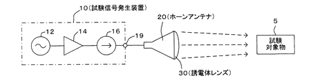
図1は、本発明が適用された実施形態の送信装置全体の構成を表す構成図である。
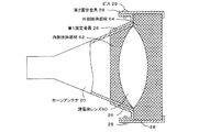
図1に示すように、本実施形態の送信装置は、妨害波による試験対象物5の耐性を測定するイミュニティ試験を行うために、試験対象物5に向けて試験用の妨害波(試験用電波)を送信するものであり、試験用電波となる試験信号を発生する試験信号発生装置10と、この試験信号発生装置10から出力される試験信号を受けて試験用電波を放射するホーンアンテナ20と、このホーンアンテナ20の開口端に固定され、ホーンアンテナ20からの試験用電波の放射特性を補正する誘電体レンズ30と、から構成されている。
Embodiments of the present invention will be described below with reference to the drawings.
FIG. 1 is a configuration diagram showing the overall configuration of a transmission apparatus according to an embodiment to which the present invention is applied.
As shown in FIG. 1, the transmission apparatus of the present embodiment performs a test interference wave (test radio wave) toward the
また、試験信号発生装置10は、例えば、国際規格「IEC61000−4−3」等で規定された放射電磁界試験を行うために、予め設定された所定周波数帯(数十MHz〜数GHz)の試験信号を発生する信号発生器12と、この信号発生器12から出力された試験信号を増幅する増幅器14と、この増幅器14にて増幅された試験信号をホーンアンテナ20が接続される出力端子19まで伝送すると共に、ホーンアンテナ20側から出力端子19に入力された信号(試験用電波の反射波の受信信号等)を減衰させて増幅器14に戻るのを阻止するアイソレータ16と、から構成されている。
In addition, the test signal generator 10 has a predetermined frequency band (several tens of MHz to several GHz) set in advance in order to perform a radiated electromagnetic field test defined by the international standard “IEC61000-4-3”, for example. A
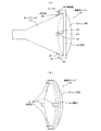
一方、誘電体レンズ30は、図2(b)に示す如く、ホーンアンテナ20の開口端部と略同径のレンズ部32と、このレンズ部32のレンズ面の外周部に形成された鍔部34と、この鍔部34に対してホーンアンテナ20の開口端周囲を囲むように突設された複数の突起部36と、から構成されている。
On the other hand, as shown in FIG. 2B, the
また、図2(a)に示す如く、ホーンアンテナ20の開口端付近の外周面には、誘電体レンズ30の鍔部34がホーンアンテナ20の開口端に当接し、且つ、突起部36がホーンアンテナ20の開口端周囲を囲むように誘電体レンズ30をホーンアンテナ20の開口端に配置した際、誘電体レンズ30の鍔部34に突設された各突起部36に当接されるように、複数のL字金具22が溶接されている。
Further, as shown in FIG. 2A, on the outer peripheral surface in the vicinity of the opening end of the
そして、これら各L字金具22と誘電体レンズ30の各突起部36には、ビス24を介して各突起部36をL字金具22に固定するためのねじ孔が穿設されており、誘電体レンズ30は、上記のようにホーンアンテナ20の開口端に固定した後、突起部36をホーンアンテナ20のL字金具22にビス止めすることにより、ホーンアンテナ20と一体化されている。なお、このように、開口端に誘電体レンズ30が固定された本実施形態のホーンアンテナ20は、本発明のEMC試験用アンテナ装置に相当する。
Each L-shaped
以上説明したように、本実施形態の送信装置においては、試験用電波を放射するホーンアンテナ20の開口端に、その試験用電波の放射特性を補正するための誘電体レンズ30を直接固定している。このため、ホーンアンテナ20からの送信電波は、誘電体レンズ30に損失なく入射することになり、従来装置のように、ホーンアンテナ20から誘電体レンズ30に至る試験用電波の伝送経路で生じる伝送損失を補うために、ホーンアンテナ20のゲインを大きくする必要はない。
As described above, in the transmission device of this embodiment, the
また、誘電体レンズ30は、ホーンアンテナ20の開口端に固定されることから、ホーンアンテナ20からの送信電波は必ず誘電体レンズ30を通って外部に放射されることになり、従来装置のように、ホーンアンテナ20からの送信電波の一部が誘電体レンズ30を通ることなく試験対象物方向に放射されてしまい、その電波がイミュニティ試験に悪影響を与えることはない。
In addition, since the
また、誘電体レンズ30は、ホーンアンテナ20の開口端と略同じ径にすればよく、従来装置のように、誘電体レンズ30の径を、ホーンアンテナ20の開口端に比べて著しく大きくする必要はない。
In addition, the
よって、本実施形態の送信装置によれば、アンテナ装置を構成しているホーンアンテナ20や誘電体レンズ30を大型化することなく、試験対象物5に対して試験用電波を適正に照射できるようになる。
Therefore, according to the transmission device of the present embodiment, the
また、本実施形態では、誘電体レンズ30のレンズ部32の外周部に鍔部34を設け、この鍔部34に突設した複数の突起部36を、ホーンアンテナ20の外周面に溶接したL字金具22にビス止めするようにしていることから、ホーンアンテナ20の開口端に誘電体レンズ30を固定する際には、鍔部34と突起部36とによりホーンアンテナ20に対してレンズ部32を正確に位置決めすることができ、しかも、位置決め後は、ビス24を用いて誘電体レンズ30をホーンアンテナ20にしっかりと固定することができる。
In the present embodiment, a flange 34 is provided on the outer periphery of the lens portion 32 of the
よって、本実施形態によれば、ホーンアンテナ20と誘電体レンズ30とから構成されるアンテナ装置の使用に伴い、ホーンアンテナ20と誘電体レンズ30との相対位置がずれて、アンテナ装置からの試験用電波の放射特性が変化してしまうといったことはなく、アンテナ装置の試験用電波の放射特性を常時最適な特性に保持することができる。
Therefore, according to the present embodiment, with the use of the antenna device composed of the
また更に、本実施形態において、試験信号発生装置10は、増幅器14にて増幅した試験信号を、方向性伝送手段としてのアイソレータ16を介して、ホーンアンテナ20に出力するように構成されていることから、ホーンアンテナ20から誘電体レンズ30を介して放射された試験用電波が試験対象物5や試験対象物5周囲の物体で反射され、その反射波が、ホーンアンテナ20にて受信されて、その受信信号が出力端子19から試験信号発生装置10内に入力されたとしても、その受信信号をアイソレータ16にて減衰させることができ、延いては、その受信信号から増幅器14を保護することができる。
Furthermore, in the present embodiment, the test signal generator 10 is configured to output the test signal amplified by the
以上、本発明の一実施形態について説明したが、本発明は、上記実施形態に限定されるものではなく、本発明の技術範囲内にて種々の態様を採ることができる。
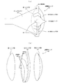
例えば、上記実施形態では、誘電体レンズ30は一つの部材からなるものとして説明したが、誘電体レンズには、ホーンアンテナ20からの放射電波が入射される表面からレンズ内に入射した放射電波を出射させる裏面にかけて複数に分割したものを使用してもよい。
As mentioned above, although one Embodiment of this invention was described, this invention is not limited to the said embodiment, A various aspect can be taken within the technical scope of this invention.
For example, in the above embodiment, the
具体的には、図3(b)に示す誘電体レンズ40は、上記実施形態の誘電体レンズ30を、ホーンアンテナ20に向けられるレンズ面を有する第1レンズ部41と、試験対象物5に向けられるレンズ面を有する第3レンズ部43と、これら第1レンズ部41と第3レンズ部43との間に位置し、上記実施形態における鍔部34を形成する第2レンズ部42とに分割したものを表しているが、このような誘電体レンズ40であっても、図3(a)に示す如く、各レンズ部41〜43を順に重ねてホーンアンテナ20の開口端部に固定するようにすれば、上記実施形態と同様のアンテナ装置を実現できる。
Specifically, the
そして、このように誘電体レンズ40を複数のレンズ部41〜43にて構成するように場合、各レンズ部41〜43毎に試験電波の透過特性を調整することができるようになり、誘電体レンズ40の調整作業を効率よく行うことができるようになる。
When the
なお、このように誘電体レンズ40を複数のレンズ部41〜43にて構成した場合には、図3(a)に示すように、各レンズ部41〜43をホーンアンテナ20の開口端に配置した後、その周囲から、粘着テープ48を用いて、各レンズ部41〜43とホーンアンテナ20とを接合するようにしてもよく、或いは、各レンズ部41〜43を接着剤を介して接合することにより一体化し、その後、上記実施形態と同様に、ビス24等を介してホーンアンテナ20の開口端に誘電体レンズ40を固定するようにしてもよい。
When the
また、この場合、粘着テープ48や接着剤には、誘電体レンズ40の電波の通過特性に影響を与えることのないよう、誘電体レンズ40と略同じ誘電率を有する材料のものを用いることが望ましく、その厚さは、試験用電波の波長の1/4以下(より好ましくは1/16以下)にすることが望ましい。
In this case, the adhesive tape 48 and the adhesive are made of materials having substantially the same dielectric constant as that of the
次に、図2及び図3に示した誘電体レンズ30、40は、レンズの表・裏面が連続する曲面で構成されているが、この場合、レンズの厚みが大きくなり過ぎ(換言すれば重くなり過ぎ)、ホーンアンテナの開口端に直接固定できなくなることも考えられる。そこで、このような場合には、図4に示す如く、誘電体レンズには、フレネルレンズからなる誘電体レンズ50を用い、これをホーンアンテナ20の開口端に固定するようにしてもよい。つまり、誘電体レンズ50をフレネルレンズにて構成すれば、レンズの厚みを小さくして、誘電体レンズ50の軽量化を図り、ホーンアンテナ20の開口端に容易に固定できるようになる。
Next, the
なお、図4に示した誘電体レンズ50は、フレネルレンズからなるレンズ部52の周囲に鍔部54を設け、この鍔部54に突設した突起部56を、ホーンアンテナ20の外周面に溶接されたL字金具22にビス止めすることにより、ホーンアンテナ20の開口端に固定できるようにされている。
The
また次に、上記実施形態では、誘電体レンズ30には、レンズ部32周囲の外周部に鍔部34を設け、この鍔部34に突設した突起部36をホーンアンテナ20に溶接されたL字金具22にビス止めすることにより、誘電体レンズ30をホーンアンテナ20に固定するものとして説明したが、例えば、図5に示すように、誘電体レンズ60を鍔部等のないレンズ部単体で構成し、その誘電体レンズ60の表・裏面を、ウレタンからなる一対の挟持部材62、64にて挟持し、一方の挟持部材(内側挟持部材)62をホーンアンテナ20の開口端から内部に収納し、他方の挟持部材(外側挟持部材64を、ホーンアンテナ20の開口よりも外側に配置することにより、誘電体レンズ60をホーンアンテナ20の開口端に固定するようにしてもよい。
Next, in the above embodiment, the
なお、この場合、内側挟持部材62は、ホーンアンテナ20の開口端付近の内壁にて保持することができるが、外側挟持部材64は、ホーンアンテナ20に直接固定することができないことから、内側挟持部材62との間で誘電体レンズ60を挟んだ状態で外側挟持部材64をホーンアンテナ20に固定するための固定具が必要になる。
In this case, the inner clamping member 62 can be held by the inner wall near the opening end of the
そして、この固定具としては、具体的には、図5に示すように、ホーンアンテナ20の開口端付近の外周面に設けられた第1固定金具26と、外側挟持部材64を収納可能な第2固定金具28とから構成し、外側挟持部材64を第2固定金具28に収納した後、ビス29を介して第2固定金具28を第1固定金具26に固定することで、誘電体レンズ60を内側挟持部材62と外側挟持部材64との間に挟んだ状態で、これら各部をホーンアンテナ20の開口端付近に位置決めできるようにすればよい。
As the fixture, specifically, as shown in FIG. 5, the
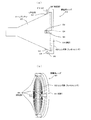
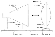
またこのように誘電体レンズをホーンアンテナの開口端に位置決めするには、必ずしも、固定用の金具やビス或いは粘着テープ等を使用する必要はなく、例えば、図6に示すように、ホーンアンテナ20及び誘電体レンズ30′を、それぞれ、支柱72a,72b若しくは支柱74aを介して、アンテナ支持台72若しくはレンズ支持台74上に固定し、更に、これら各支持台72,74を、スライドレール70上にスライド可能に配置して、スライドレール70上で移動させることにより、誘電体レンズ30′をホーンアンテナ20の開口端に位置決めするようにしてもよい。
Further, in order to position the dielectric lens at the opening end of the horn antenna in this manner, it is not always necessary to use a fixing bracket, a screw, an adhesive tape, or the like. For example, as shown in FIG. And the
そして、このようにすれば、アンテナ支持台72及びレンズ支持台74を介してスライドレール70上に載置するホーンアンテナ20や誘電体レンズ30を変更することにより、EMC試験(詳しくはイミュニティ試験)を行うのに用いるホーンアンテナ20と誘電体レンズ30′との組み合わせを簡単に変更することができるようになる。
In this way, by changing the
なお、図6において、誘電体レンズ30′は、図2に示した誘電体レンズ30からビス止め用の突起部36を削除したものとなっており、レンズ支持台74から突出した支柱74aを誘電体レンズ30′の鍔部34に接合することにより、レンズ支持台74(延いてはスライドレール70)上に載置されている。
In FIG. 6, a dielectric lens 30 'is obtained by removing the screw-fixing
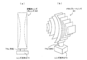
一方、上記実施形態では、ホーンアンテナ20の開口端に配置する放射特性補正レンズは、凸レンズ形状に形成された誘電体レンズ30,40,60、若しくは、フレネルレンズとして形成された誘電体レンズ50であるものとして説明したが、本発明の放射特性補正レンズとしては、図7(a)に示すように凹レンズ形状に形成された誘電体レンズ80であっても、或いは、図7(b)に示すように、複数の金属板(メタルプレート)を所定の間隔を開けて平行に配置したメタルプレートレンズ90であってもよい。
On the other hand, in the above embodiment, the radiation characteristic correction lens disposed at the opening end of the
なお、図7において、上記各レンズ80、90は、図6に示したスライドレール70に載置してホーンアンテナ20の開口端に配置できるように、支柱74aを介してレンズ支持台74上に固定されているものとして記載されているが、これら各アンプは、図5に示したように挟持部材62、64を利用してホーンアンテナ20の開口端に配置するようにしてもよく、或いは、各レンズ80、90の周囲に合成樹脂等からなる鍔部を設けて、ホーンアンテナ20の開口端に位置決め固定するようにしてもよい。
In FIG. 7, each of the lenses 80 and 90 is placed on the lens support 74 via a support 74a so that it can be placed on the slide rail 70 shown in FIG. Although described as being fixed, each of these amplifiers may be arranged at the open end of the
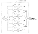
また、上記実施形態では、試験信号発生装置10には、試験信号を増幅する増幅器14と、この増幅器14にて増幅された試験信号をホーンアンテナ20側に出力するアイソレータ16とが、夫々、1個設けられるものとして説明したが、例えば、図8に示すように、試験信号発生装置10には、増幅器14及びアイソレータ16を複数対(図では8対)設け、信号発生器12から出力された試験信号は、分配器13にて複数に分配(図では8分配)して各増幅器14に出力入力するようにし、各増幅器14にて増幅された試験信号については、各増幅器14に対応するアイソレータ16を介して、合成器18に入力することにより、合成器18にて合成し、出力端子19からホーンアンテナ20へ出力するように構成してもよい。
In the above embodiment, the test signal generator 10 includes an
なお、図8において、試験信号発生装置10には、合成器18として、8個の増幅器14にて夫々増幅された8系統の試験信号の内、互いに隣接する2つの増幅器14にて増幅された試験信号同士を夫々合成する4個の合成器18と、これら4個の合成器18にて合成された4系統の試験信号の内、互いに隣接する2つの合成器18にて合成された試験信号同士を夫々合成する2個の合成器18と、この2個の合成器18にて合成された2系統の試験信号同士を合成する1個の合成器18との、合計7個の合成器が設けられている。
In FIG. 8, the test signal generator 10 is amplified by the two
そして、試験信号発生装置10を、図8に示す如く構成した場合には、ホーンアンテナ20から誘電体レンズ30、40、50、60等を介して送信した試験用電波の反射波が高レベルとなり、ホーンアンテナ20から試験信号発生装置10に入力される受信信号の信号レベルが著しく高レベルになったとしても、その受信信号は、合成器18にて分配され、更に、アイソレータ16にて減衰されることから、各増幅器14に入力される受信信号の信号レベルは充分低くなり、各増幅器14がその受信信号によって故障するのをより確実に防止することができる。
When the test signal generator 10 is configured as shown in FIG. 8, the reflected wave of the test radio wave transmitted from the
また、試験信号発生装置10を、図8に示す如く構成した場合には、複数の増幅器14にて増幅した試験信号を合成してホーンアンテナ20に出力することができるため、増幅器14の1台当たりの送信パワーは、図1に示した試験信号発生装置10の増幅器14の1/8にすることができ、延いては、試験信号発生装置10を低コストで実現できるようになる。
Further, when the test signal generator 10 is configured as shown in FIG. 8, the test signals amplified by the plurality of
5…試験対象物、10…試験信号発生装置、12…信号発生器、13…分配器、14…増幅器、16…アイソレータ、18…合成器、19…出力端子、20…ホーンアンテナ、22…L字金具、24,29…ビス、26…第1固定金具、28…第2固定金具、30,30′,40,50,60,80…誘電体レンズ、32,52…レンズ部、34,54…鍔部、36,56…突起部、41…第1レンズ部、42…第2レンズ部、43…第3レンズ部、48…粘着テープ、62…内側挟持部材、64…外側挟持部材、70…スライドレール、72…アンテナ支持台、74…レンズ支持台、72a,72b,74a…支柱、90…メタルプレートレンズ。
DESCRIPTION OF
Claims (17)
前記試験対象物に向けて試験用電波を放射するホーンアンテナと、
該ホーンアンテナからの試験用電波の放射特性を補正する放射特性補正レンズと、
を備え、該放射特性補正レンズを前記ホーンアンテナの開口端に配置してなることを特徴とするEMC試験用アンテナ装置。 An antenna device used for conducting an EMC test of a test object,
A horn antenna that radiates test radio waves toward the test object;
A radiation characteristic correcting lens for correcting the radiation characteristic of the test radio wave from the horn antenna;
An EMC test antenna device, characterized in that the radiation characteristic correcting lens is disposed at an opening end of the horn antenna.
前記放射特性補正レンズは、
前記一対の挟持部材の一方を前記ホーンアンテナの内部に収納し、他方の挟持部材を、当該放射特性補正レンズを挟んで前記ホーンアンテナの外側に配置し、更に、該他方の挟持部材を固定部材を介して前記ホーンアンテナに固定することにより、前記ホーンアンテナの開口端に配置されていることを特徴とする請求項1〜請求項6の何れかに記載のEMC試験用アンテナ装置。 It is composed of a material that can transmit a test radio wave, and includes a pair of clamping members that are in contact with the front and back surfaces of the radiation characteristic correction lens and sandwich the radiation characteristic correction lens, respectively.
The radiation characteristic correction lens is
One of the pair of sandwiching members is housed inside the horn antenna, the other sandwiching member is disposed outside the horn antenna with the radiation characteristic correcting lens sandwiched therebetween, and the other sandwiching member is fixed to the fixing member. The antenna device for EMC testing according to any one of claims 1 to 6, wherein the antenna device for EMC testing is disposed at an opening end of the horn antenna by being fixed to the horn antenna via a pin.
前記放射特性補正レンズは、該支持部材を介して、前記ホーンアンテナの開口端に配置されていることを特徴とする請求項1〜請求項6の何れかに記載のEMC試験用アンテナ装置。 The horn antenna and the radiation characteristic correction lens each include a support member that supports the opening end of the horn antenna and the lens surface of the radiation characteristic correction lens so as to be able to contact and separate,
The EMC test antenna device according to any one of claims 1 to 6, wherein the radiation characteristic correction lens is disposed at an opening end of the horn antenna via the support member.
前記試験信号を発生する信号発生器と、
該信号発生器から出力された試験信号を増幅する増幅器と、
該増幅器にて増幅された試験信号を前記EMC試験用アンテナ装置が接続される出力端子まで伝送すると共に、該出力端子に外部から入力された高周波信号が前記増幅器に戻るのを阻止する方向性伝送手段と、
を備えたことを特徴とする試験信号発生装置。 A test signal for an immunity test for measuring the resistance of a test object due to an interference wave is generated and output to the EMC test antenna device according to any one of claims 1 to 14, thereby A test signal generator for radiating the interference wave from an antenna device toward the test object,
A signal generator for generating the test signal;
An amplifier for amplifying the test signal output from the signal generator;
A directional transmission for transmitting a test signal amplified by the amplifier to an output terminal to which the EMC test antenna device is connected and preventing a high-frequency signal input from the outside to the output terminal from returning to the amplifier. Means,
A test signal generator characterized by comprising:
前記信号発生器から出力された試験信号を複数に分配して前記各増幅器に出力する分配器と、
前記各増幅器にて増幅され、各増幅器に対応する各方向性伝送手段から出力される複数の試験信号を合成して、前記出力端子に出力する合成器と、
を備えたことを特徴とする請求項17に記載の試験信号発生装置。 A plurality of pairs of amplifiers and directional transmission means;
A distributor for distributing a plurality of test signals output from the signal generator to the amplifiers;
A synthesizer that synthesizes a plurality of test signals that are amplified by each amplifier and output from each directional transmission means corresponding to each amplifier, and outputs to the output terminal;
The test signal generator according to claim 17, further comprising:
請求項1〜請求項14の何れかに記載のEMC試験用アンテナ装置と、
請求項15又は請求項16に記載の試験信号発生装置と、
を備えたことを特徴とする送信装置。 A transmitter for transmitting a test interference wave toward the test object in order to perform an immunity test for measuring the resistance of the test object due to the interference wave;
The EMC test antenna device according to any one of claims 1 to 14,
A test signal generator according to claim 15 or 16, and
A transmission device comprising:
Priority Applications (1)
| Application Number | Priority Date | Filing Date | Title |
|---|---|---|---|
| JP2005104826A JP2006166399A (en) | 2004-11-15 | 2005-03-31 | EMC test antenna device, test signal generator, and transmitter |
Applications Claiming Priority (2)
| Application Number | Priority Date | Filing Date | Title |
|---|---|---|---|
| JP2004330827 | 2004-11-15 | ||
| JP2005104826A JP2006166399A (en) | 2004-11-15 | 2005-03-31 | EMC test antenna device, test signal generator, and transmitter |
Publications (1)
| Publication Number | Publication Date |
|---|---|
| JP2006166399A true JP2006166399A (en) | 2006-06-22 |
Family
ID=36667842
Family Applications (1)
| Application Number | Title | Priority Date | Filing Date |
|---|---|---|---|
| JP2005104826A Pending JP2006166399A (en) | 2004-11-15 | 2005-03-31 | EMC test antenna device, test signal generator, and transmitter |
Country Status (1)
| Country | Link |
|---|---|
| JP (1) | JP2006166399A (en) |
Cited By (170)
| Publication number | Priority date | Publication date | Assignee | Title |
|---|---|---|---|---|
| DE102013108434A1 (en) * | 2013-08-05 | 2015-02-26 | Finetek Co., Ltd. | Horn antenna device and stepped signal input device therefor |
| US20160056523A1 (en) * | 2013-04-02 | 2016-02-25 | Telefonaktiebolaget L M Ericsson (Publ) | Radio Antenna Positioning |
| US9312919B1 (en) | 2014-10-21 | 2016-04-12 | At&T Intellectual Property I, Lp | Transmission device with impairment compensation and methods for use therewith |
| US9461706B1 (en) | 2015-07-31 | 2016-10-04 | At&T Intellectual Property I, Lp | Method and apparatus for exchanging communication signals |
| US9467870B2 (en) | 2013-11-06 | 2016-10-11 | At&T Intellectual Property I, L.P. | Surface-wave communications and methods thereof |
| US9479266B2 (en) | 2013-12-10 | 2016-10-25 | At&T Intellectual Property I, L.P. | Quasi-optical coupler |
| US9490869B1 (en) | 2015-05-14 | 2016-11-08 | At&T Intellectual Property I, L.P. | Transmission medium having multiple cores and methods for use therewith |
| US9503189B2 (en) | 2014-10-10 | 2016-11-22 | At&T Intellectual Property I, L.P. | Method and apparatus for arranging communication sessions in a communication system |
| US9520945B2 (en) | 2014-10-21 | 2016-12-13 | At&T Intellectual Property I, L.P. | Apparatus for providing communication services and methods thereof |
| US9525524B2 (en) | 2013-05-31 | 2016-12-20 | At&T Intellectual Property I, L.P. | Remote distributed antenna system |
| US9525210B2 (en) | 2014-10-21 | 2016-12-20 | At&T Intellectual Property I, L.P. | Guided-wave transmission device with non-fundamental mode propagation and methods for use therewith |
| US9531427B2 (en) | 2014-11-20 | 2016-12-27 | At&T Intellectual Property I, L.P. | Transmission device with mode division multiplexing and methods for use therewith |
| US9564947B2 (en) | 2014-10-21 | 2017-02-07 | At&T Intellectual Property I, L.P. | Guided-wave transmission device with diversity and methods for use therewith |
| US9577307B2 (en) | 2014-10-21 | 2017-02-21 | At&T Intellectual Property I, L.P. | Guided-wave transmission device and methods for use therewith |
| US9608692B2 (en) | 2015-06-11 | 2017-03-28 | At&T Intellectual Property I, L.P. | Repeater and methods for use therewith |
| US9608740B2 (en) | 2015-07-15 | 2017-03-28 | At&T Intellectual Property I, L.P. | Method and apparatus for launching a wave mode that mitigates interference |
| US9615269B2 (en) | 2014-10-02 | 2017-04-04 | At&T Intellectual Property I, L.P. | Method and apparatus that provides fault tolerance in a communication network |
| US9628854B2 (en) | 2014-09-29 | 2017-04-18 | At&T Intellectual Property I, L.P. | Method and apparatus for distributing content in a communication network |
| US9628116B2 (en) | 2015-07-14 | 2017-04-18 | At&T Intellectual Property I, L.P. | Apparatus and methods for transmitting wireless signals |
| US9640850B2 (en) | 2015-06-25 | 2017-05-02 | At&T Intellectual Property I, L.P. | Methods and apparatus for inducing a non-fundamental wave mode on a transmission medium |
| US9654173B2 (en) | 2014-11-20 | 2017-05-16 | At&T Intellectual Property I, L.P. | Apparatus for powering a communication device and methods thereof |
| US9653770B2 (en) | 2014-10-21 | 2017-05-16 | At&T Intellectual Property I, L.P. | Guided wave coupler, coupling module and methods for use therewith |
| US9667317B2 (en) | 2015-06-15 | 2017-05-30 | At&T Intellectual Property I, L.P. | Method and apparatus for providing security using network traffic adjustments |
| US9680670B2 (en) | 2014-11-20 | 2017-06-13 | At&T Intellectual Property I, L.P. | Transmission device with channel equalization and control and methods for use therewith |
| US9685992B2 (en) | 2014-10-03 | 2017-06-20 | At&T Intellectual Property I, L.P. | Circuit panel network and methods thereof |
| US9692101B2 (en) | 2014-08-26 | 2017-06-27 | At&T Intellectual Property I, L.P. | Guided wave couplers for coupling electromagnetic waves between a waveguide surface and a surface of a wire |
| US9699785B2 (en) | 2012-12-05 | 2017-07-04 | At&T Intellectual Property I, L.P. | Backhaul link for distributed antenna system |
| US9705561B2 (en) | 2015-04-24 | 2017-07-11 | At&T Intellectual Property I, L.P. | Directional coupling device and methods for use therewith |
| US9722318B2 (en) | 2015-07-14 | 2017-08-01 | At&T Intellectual Property I, L.P. | Method and apparatus for coupling an antenna to a device |
| US9729197B2 (en) | 2015-10-01 | 2017-08-08 | At&T Intellectual Property I, L.P. | Method and apparatus for communicating network management traffic over a network |
| US9735833B2 (en) | 2015-07-31 | 2017-08-15 | At&T Intellectual Property I, L.P. | Method and apparatus for communications management in a neighborhood network |
| US9742462B2 (en) | 2014-12-04 | 2017-08-22 | At&T Intellectual Property I, L.P. | Transmission medium and communication interfaces and methods for use therewith |
| US9749053B2 (en) | 2015-07-23 | 2017-08-29 | At&T Intellectual Property I, L.P. | Node device, repeater and methods for use therewith |
| US9749013B2 (en) | 2015-03-17 | 2017-08-29 | At&T Intellectual Property I, L.P. | Method and apparatus for reducing attenuation of electromagnetic waves guided by a transmission medium |
| US9748626B2 (en) | 2015-05-14 | 2017-08-29 | At&T Intellectual Property I, L.P. | Plurality of cables having different cross-sectional shapes which are bundled together to form a transmission medium |
| US9755697B2 (en) | 2014-09-15 | 2017-09-05 | At&T Intellectual Property I, L.P. | Method and apparatus for sensing a condition in a transmission medium of electromagnetic waves |
| US9762289B2 (en) | 2014-10-14 | 2017-09-12 | At&T Intellectual Property I, L.P. | Method and apparatus for transmitting or receiving signals in a transportation system |
| US9769020B2 (en) | 2014-10-21 | 2017-09-19 | At&T Intellectual Property I, L.P. | Method and apparatus for responding to events affecting communications in a communication network |
| US9769128B2 (en) | 2015-09-28 | 2017-09-19 | At&T Intellectual Property I, L.P. | Method and apparatus for encryption of communications over a network |
| US9780834B2 (en) | 2014-10-21 | 2017-10-03 | At&T Intellectual Property I, L.P. | Method and apparatus for transmitting electromagnetic waves |
| US9787412B2 (en) | 2015-06-25 | 2017-10-10 | At&T Intellectual Property I, L.P. | Methods and apparatus for inducing a fundamental wave mode on a transmission medium |
| US9793954B2 (en) | 2015-04-28 | 2017-10-17 | At&T Intellectual Property I, L.P. | Magnetic coupling device and methods for use therewith |
| US9793951B2 (en) | 2015-07-15 | 2017-10-17 | At&T Intellectual Property I, L.P. | Method and apparatus for launching a wave mode that mitigates interference |
| US9793955B2 (en) | 2015-04-24 | 2017-10-17 | At&T Intellectual Property I, Lp | Passive electrical coupling device and methods for use therewith |
| US9800327B2 (en) | 2014-11-20 | 2017-10-24 | At&T Intellectual Property I, L.P. | Apparatus for controlling operations of a communication device and methods thereof |
| US9820146B2 (en) | 2015-06-12 | 2017-11-14 | At&T Intellectual Property I, L.P. | Method and apparatus for authentication and identity management of communicating devices |
| US9838896B1 (en) | 2016-12-09 | 2017-12-05 | At&T Intellectual Property I, L.P. | Method and apparatus for assessing network coverage |
| US9836957B2 (en) | 2015-07-14 | 2017-12-05 | At&T Intellectual Property I, L.P. | Method and apparatus for communicating with premises equipment |
| US9847850B2 (en) | 2014-10-14 | 2017-12-19 | At&T Intellectual Property I, L.P. | Method and apparatus for adjusting a mode of communication in a communication network |
| US9847566B2 (en) | 2015-07-14 | 2017-12-19 | At&T Intellectual Property I, L.P. | Method and apparatus for adjusting a field of a signal to mitigate interference |
| US9853342B2 (en) | 2015-07-14 | 2017-12-26 | At&T Intellectual Property I, L.P. | Dielectric transmission medium connector and methods for use therewith |
| US9860075B1 (en) | 2016-08-26 | 2018-01-02 | At&T Intellectual Property I, L.P. | Method and communication node for broadband distribution |
| US9865911B2 (en) | 2015-06-25 | 2018-01-09 | At&T Intellectual Property I, L.P. | Waveguide system for slot radiating first electromagnetic waves that are combined into a non-fundamental wave mode second electromagnetic wave on a transmission medium |
| US9866309B2 (en) | 2015-06-03 | 2018-01-09 | At&T Intellectual Property I, Lp | Host node device and methods for use therewith |
| US9871283B2 (en) | 2015-07-23 | 2018-01-16 | At&T Intellectual Property I, Lp | Transmission medium having a dielectric core comprised of plural members connected by a ball and socket configuration |
| US9871282B2 (en) | 2015-05-14 | 2018-01-16 | At&T Intellectual Property I, L.P. | At least one transmission medium having a dielectric surface that is covered at least in part by a second dielectric |
| US9876264B2 (en) | 2015-10-02 | 2018-01-23 | At&T Intellectual Property I, Lp | Communication system, guided wave switch and methods for use therewith |
| US9876571B2 (en) | 2015-02-20 | 2018-01-23 | At&T Intellectual Property I, Lp | Guided-wave transmission device with non-fundamental mode propagation and methods for use therewith |
| US9876605B1 (en) | 2016-10-21 | 2018-01-23 | At&T Intellectual Property I, L.P. | Launcher and coupling system to support desired guided wave mode |
| US9882257B2 (en) | 2015-07-14 | 2018-01-30 | At&T Intellectual Property I, L.P. | Method and apparatus for launching a wave mode that mitigates interference |
| US9882277B2 (en) | 2015-10-02 | 2018-01-30 | At&T Intellectual Property I, Lp | Communication device and antenna assembly with actuated gimbal mount |
| US9893795B1 (en) | 2016-12-07 | 2018-02-13 | At&T Intellectual Property I, Lp | Method and repeater for broadband distribution |
| US9906269B2 (en) | 2014-09-17 | 2018-02-27 | At&T Intellectual Property I, L.P. | Monitoring and mitigating conditions in a communication network |
| US9904535B2 (en) | 2015-09-14 | 2018-02-27 | At&T Intellectual Property I, L.P. | Method and apparatus for distributing software |
| US9912419B1 (en) | 2016-08-24 | 2018-03-06 | At&T Intellectual Property I, L.P. | Method and apparatus for managing a fault in a distributed antenna system |
| US9912382B2 (en) | 2015-06-03 | 2018-03-06 | At&T Intellectual Property I, Lp | Network termination and methods for use therewith |
| US9912027B2 (en) | 2015-07-23 | 2018-03-06 | At&T Intellectual Property I, L.P. | Method and apparatus for exchanging communication signals |
| US9911020B1 (en) | 2016-12-08 | 2018-03-06 | At&T Intellectual Property I, L.P. | Method and apparatus for tracking via a radio frequency identification device |
| US9913139B2 (en) | 2015-06-09 | 2018-03-06 | At&T Intellectual Property I, L.P. | Signal fingerprinting for authentication of communicating devices |
| US9917341B2 (en) | 2015-05-27 | 2018-03-13 | At&T Intellectual Property I, L.P. | Apparatus and method for launching electromagnetic waves and for modifying radial dimensions of the propagating electromagnetic waves |
| US9927517B1 (en) | 2016-12-06 | 2018-03-27 | At&T Intellectual Property I, L.P. | Apparatus and methods for sensing rainfall |
| US9948354B2 (en) | 2015-04-28 | 2018-04-17 | At&T Intellectual Property I, L.P. | Magnetic coupling device with reflective plate and methods for use therewith |
| US9948333B2 (en) | 2015-07-23 | 2018-04-17 | At&T Intellectual Property I, L.P. | Method and apparatus for wireless communications to mitigate interference |
| WO2018070566A1 (en) * | 2016-10-12 | 2018-04-19 | 위월드 주식회사 | Horn array antenna including dielectric cover |
| US9954287B2 (en) | 2014-11-20 | 2018-04-24 | At&T Intellectual Property I, L.P. | Apparatus for converting wireless signals and electromagnetic waves and methods thereof |
| US9967173B2 (en) | 2015-07-31 | 2018-05-08 | At&T Intellectual Property I, L.P. | Method and apparatus for authentication and identity management of communicating devices |
| US9973940B1 (en) | 2017-02-27 | 2018-05-15 | At&T Intellectual Property I, L.P. | Apparatus and methods for dynamic impedance matching of a guided wave launcher |
| WO2018087982A1 (en) * | 2016-11-09 | 2018-05-17 | 日本電気株式会社 | Communication device |
| US9991580B2 (en) | 2016-10-21 | 2018-06-05 | At&T Intellectual Property I, L.P. | Launcher and coupling system for guided wave mode cancellation |
| US9997819B2 (en) | 2015-06-09 | 2018-06-12 | At&T Intellectual Property I, L.P. | Transmission medium and method for facilitating propagation of electromagnetic waves via a core |
| US9999038B2 (en) | 2013-05-31 | 2018-06-12 | At&T Intellectual Property I, L.P. | Remote distributed antenna system |
| US9998870B1 (en) | 2016-12-08 | 2018-06-12 | At&T Intellectual Property I, L.P. | Method and apparatus for proximity sensing |
| US10009065B2 (en) | 2012-12-05 | 2018-06-26 | At&T Intellectual Property I, L.P. | Backhaul link for distributed antenna system |
| US10009901B2 (en) | 2015-09-16 | 2018-06-26 | At&T Intellectual Property I, L.P. | Method, apparatus, and computer-readable storage medium for managing utilization of wireless resources between base stations |
| US10009063B2 (en) | 2015-09-16 | 2018-06-26 | At&T Intellectual Property I, L.P. | Method and apparatus for use with a radio distributed antenna system having an out-of-band reference signal |
| US10009067B2 (en) | 2014-12-04 | 2018-06-26 | At&T Intellectual Property I, L.P. | Method and apparatus for configuring a communication interface |
| US10020587B2 (en) | 2015-07-31 | 2018-07-10 | At&T Intellectual Property I, L.P. | Radial antenna and methods for use therewith |
| US10020844B2 (en) | 2016-12-06 | 2018-07-10 | T&T Intellectual Property I, L.P. | Method and apparatus for broadcast communication via guided waves |
| US10027397B2 (en) | 2016-12-07 | 2018-07-17 | At&T Intellectual Property I, L.P. | Distributed antenna system and methods for use therewith |
| US10033108B2 (en) | 2015-07-14 | 2018-07-24 | At&T Intellectual Property I, L.P. | Apparatus and methods for generating an electromagnetic wave having a wave mode that mitigates interference |
| US10033107B2 (en) | 2015-07-14 | 2018-07-24 | At&T Intellectual Property I, L.P. | Method and apparatus for coupling an antenna to a device |
| US10044409B2 (en) | 2015-07-14 | 2018-08-07 | At&T Intellectual Property I, L.P. | Transmission medium and methods for use therewith |
| US10051483B2 (en) | 2015-10-16 | 2018-08-14 | At&T Intellectual Property I, L.P. | Method and apparatus for directing wireless signals |
| US10051629B2 (en) | 2015-09-16 | 2018-08-14 | At&T Intellectual Property I, L.P. | Method and apparatus for use with a radio distributed antenna system having an in-band reference signal |
| US10069535B2 (en) | 2016-12-08 | 2018-09-04 | At&T Intellectual Property I, L.P. | Apparatus and methods for launching electromagnetic waves having a certain electric field structure |
| US10074890B2 (en) | 2015-10-02 | 2018-09-11 | At&T Intellectual Property I, L.P. | Communication device and antenna with integrated light assembly |
| US10079661B2 (en) | 2015-09-16 | 2018-09-18 | At&T Intellectual Property I, L.P. | Method and apparatus for use with a radio distributed antenna system having a clock reference |
| US10090594B2 (en) | 2016-11-23 | 2018-10-02 | At&T Intellectual Property I, L.P. | Antenna system having structural configurations for assembly |
| US10090606B2 (en) | 2015-07-15 | 2018-10-02 | At&T Intellectual Property I, L.P. | Antenna system with dielectric array and methods for use therewith |
| US10103422B2 (en) | 2016-12-08 | 2018-10-16 | At&T Intellectual Property I, L.P. | Method and apparatus for mounting network devices |
| US10103801B2 (en) | 2015-06-03 | 2018-10-16 | At&T Intellectual Property I, L.P. | Host node device and methods for use therewith |
| US10135146B2 (en) | 2016-10-18 | 2018-11-20 | At&T Intellectual Property I, L.P. | Apparatus and methods for launching guided waves via circuits |
| US10135147B2 (en) | 2016-10-18 | 2018-11-20 | At&T Intellectual Property I, L.P. | Apparatus and methods for launching guided waves via an antenna |
| US10136434B2 (en) | 2015-09-16 | 2018-11-20 | At&T Intellectual Property I, L.P. | Method and apparatus for use with a radio distributed antenna system having an ultra-wideband control channel |
| US10135145B2 (en) | 2016-12-06 | 2018-11-20 | At&T Intellectual Property I, L.P. | Apparatus and methods for generating an electromagnetic wave along a transmission medium |
| US10142086B2 (en) | 2015-06-11 | 2018-11-27 | At&T Intellectual Property I, L.P. | Repeater and methods for use therewith |
| US10139820B2 (en) | 2016-12-07 | 2018-11-27 | At&T Intellectual Property I, L.P. | Method and apparatus for deploying equipment of a communication system |
| US10144036B2 (en) | 2015-01-30 | 2018-12-04 | At&T Intellectual Property I, L.P. | Method and apparatus for mitigating interference affecting a propagation of electromagnetic waves guided by a transmission medium |
| US10148016B2 (en) | 2015-07-14 | 2018-12-04 | At&T Intellectual Property I, L.P. | Apparatus and methods for communicating utilizing an antenna array |
| US10154493B2 (en) | 2015-06-03 | 2018-12-11 | At&T Intellectual Property I, L.P. | Network termination and methods for use therewith |
| US10168695B2 (en) | 2016-12-07 | 2019-01-01 | At&T Intellectual Property I, L.P. | Method and apparatus for controlling an unmanned aircraft |
| US10170840B2 (en) | 2015-07-14 | 2019-01-01 | At&T Intellectual Property I, L.P. | Apparatus and methods for sending or receiving electromagnetic signals |
| US10178445B2 (en) | 2016-11-23 | 2019-01-08 | At&T Intellectual Property I, L.P. | Methods, devices, and systems for load balancing between a plurality of waveguides |
| US10205655B2 (en) | 2015-07-14 | 2019-02-12 | At&T Intellectual Property I, L.P. | Apparatus and methods for communicating utilizing an antenna array and multiple communication paths |
| US10224634B2 (en) | 2016-11-03 | 2019-03-05 | At&T Intellectual Property I, L.P. | Methods and apparatus for adjusting an operational characteristic of an antenna |
| US10225025B2 (en) | 2016-11-03 | 2019-03-05 | At&T Intellectual Property I, L.P. | Method and apparatus for detecting a fault in a communication system |
| US10243784B2 (en) | 2014-11-20 | 2019-03-26 | At&T Intellectual Property I, L.P. | System for generating topology information and methods thereof |
| US10243270B2 (en) | 2016-12-07 | 2019-03-26 | At&T Intellectual Property I, L.P. | Beam adaptive multi-feed dielectric antenna system and methods for use therewith |
| US10264586B2 (en) | 2016-12-09 | 2019-04-16 | At&T Mobility Ii Llc | Cloud-based packet controller and methods for use therewith |
| US10291334B2 (en) | 2016-11-03 | 2019-05-14 | At&T Intellectual Property I, L.P. | System for detecting a fault in a communication system |
| US10291311B2 (en) | 2016-09-09 | 2019-05-14 | At&T Intellectual Property I, L.P. | Method and apparatus for mitigating a fault in a distributed antenna system |
| US10298293B2 (en) | 2017-03-13 | 2019-05-21 | At&T Intellectual Property I, L.P. | Apparatus of communication utilizing wireless network devices |
| US10305190B2 (en) | 2016-12-01 | 2019-05-28 | At&T Intellectual Property I, L.P. | Reflecting dielectric antenna system and methods for use therewith |
| US10312567B2 (en) | 2016-10-26 | 2019-06-04 | At&T Intellectual Property I, L.P. | Launcher with planar strip antenna and methods for use therewith |
| US10320586B2 (en) | 2015-07-14 | 2019-06-11 | At&T Intellectual Property I, L.P. | Apparatus and methods for generating non-interfering electromagnetic waves on an insulated transmission medium |
| US10326494B2 (en) | 2016-12-06 | 2019-06-18 | At&T Intellectual Property I, L.P. | Apparatus for measurement de-embedding and methods for use therewith |
| US10326689B2 (en) | 2016-12-08 | 2019-06-18 | At&T Intellectual Property I, L.P. | Method and system for providing alternative communication paths |
| US10340983B2 (en) | 2016-12-09 | 2019-07-02 | At&T Intellectual Property I, L.P. | Method and apparatus for surveying remote sites via guided wave communications |
| US10340600B2 (en) | 2016-10-18 | 2019-07-02 | At&T Intellectual Property I, L.P. | Apparatus and methods for launching guided waves via plural waveguide systems |
| US10341142B2 (en) | 2015-07-14 | 2019-07-02 | At&T Intellectual Property I, L.P. | Apparatus and methods for generating non-interfering electromagnetic waves on an uninsulated conductor |
| US10340601B2 (en) | 2016-11-23 | 2019-07-02 | At&T Intellectual Property I, L.P. | Multi-antenna system and methods for use therewith |
| US10340603B2 (en) | 2016-11-23 | 2019-07-02 | At&T Intellectual Property I, L.P. | Antenna system having shielded structural configurations for assembly |
| US10340573B2 (en) | 2016-10-26 | 2019-07-02 | At&T Intellectual Property I, L.P. | Launcher with cylindrical coupling device and methods for use therewith |
| US10348391B2 (en) | 2015-06-03 | 2019-07-09 | At&T Intellectual Property I, L.P. | Client node device with frequency conversion and methods for use therewith |
| US10355367B2 (en) | 2015-10-16 | 2019-07-16 | At&T Intellectual Property I, L.P. | Antenna structure for exchanging wireless signals |
| US10359749B2 (en) | 2016-12-07 | 2019-07-23 | At&T Intellectual Property I, L.P. | Method and apparatus for utilities management via guided wave communication |
| US10361489B2 (en) | 2016-12-01 | 2019-07-23 | At&T Intellectual Property I, L.P. | Dielectric dish antenna system and methods for use therewith |
| US10374316B2 (en) | 2016-10-21 | 2019-08-06 | At&T Intellectual Property I, L.P. | System and dielectric antenna with non-uniform dielectric |
| US10382976B2 (en) | 2016-12-06 | 2019-08-13 | At&T Intellectual Property I, L.P. | Method and apparatus for managing wireless communications based on communication paths and network device positions |
| US10389037B2 (en) | 2016-12-08 | 2019-08-20 | At&T Intellectual Property I, L.P. | Apparatus and methods for selecting sections of an antenna array and use therewith |
| US10389029B2 (en) | 2016-12-07 | 2019-08-20 | At&T Intellectual Property I, L.P. | Multi-feed dielectric antenna system with core selection and methods for use therewith |
| US10396887B2 (en) | 2015-06-03 | 2019-08-27 | At&T Intellectual Property I, L.P. | Client node device and methods for use therewith |
| US10411356B2 (en) | 2016-12-08 | 2019-09-10 | At&T Intellectual Property I, L.P. | Apparatus and methods for selectively targeting communication devices with an antenna array |
| US10439675B2 (en) | 2016-12-06 | 2019-10-08 | At&T Intellectual Property I, L.P. | Method and apparatus for repeating guided wave communication signals |
| US10446936B2 (en) | 2016-12-07 | 2019-10-15 | At&T Intellectual Property I, L.P. | Multi-feed dielectric antenna system and methods for use therewith |
| US10498044B2 (en) | 2016-11-03 | 2019-12-03 | At&T Intellectual Property I, L.P. | Apparatus for configuring a surface of an antenna |
| US10530505B2 (en) | 2016-12-08 | 2020-01-07 | At&T Intellectual Property I, L.P. | Apparatus and methods for launching electromagnetic waves along a transmission medium |
| US10535928B2 (en) | 2016-11-23 | 2020-01-14 | At&T Intellectual Property I, L.P. | Antenna system and methods for use therewith |
| US10547348B2 (en) | 2016-12-07 | 2020-01-28 | At&T Intellectual Property I, L.P. | Method and apparatus for switching transmission mediums in a communication system |
| US10601494B2 (en) | 2016-12-08 | 2020-03-24 | At&T Intellectual Property I, L.P. | Dual-band communication device and method for use therewith |
| US10637149B2 (en) | 2016-12-06 | 2020-04-28 | At&T Intellectual Property I, L.P. | Injection molded dielectric antenna and methods for use therewith |
| US10650940B2 (en) | 2015-05-15 | 2020-05-12 | At&T Intellectual Property I, L.P. | Transmission medium having a conductive material and methods for use therewith |
| US10665942B2 (en) | 2015-10-16 | 2020-05-26 | At&T Intellectual Property I, L.P. | Method and apparatus for adjusting wireless communications |
| US10679767B2 (en) | 2015-05-15 | 2020-06-09 | At&T Intellectual Property I, L.P. | Transmission medium having a conductive material and methods for use therewith |
| US10694379B2 (en) | 2016-12-06 | 2020-06-23 | At&T Intellectual Property I, L.P. | Waveguide system with device-based authentication and methods for use therewith |
| US10727599B2 (en) | 2016-12-06 | 2020-07-28 | At&T Intellectual Property I, L.P. | Launcher with slot antenna and methods for use therewith |
| US10755542B2 (en) | 2016-12-06 | 2020-08-25 | At&T Intellectual Property I, L.P. | Method and apparatus for surveillance via guided wave communication |
| US10777873B2 (en) | 2016-12-08 | 2020-09-15 | At&T Intellectual Property I, L.P. | Method and apparatus for mounting network devices |
| US10784670B2 (en) | 2015-07-23 | 2020-09-22 | At&T Intellectual Property I, L.P. | Antenna support for aligning an antenna |
| US10811767B2 (en) | 2016-10-21 | 2020-10-20 | At&T Intellectual Property I, L.P. | System and dielectric antenna with convex dielectric radome |
| US10819035B2 (en) | 2016-12-06 | 2020-10-27 | At&T Intellectual Property I, L.P. | Launcher with helical antenna and methods for use therewith |
| US10916969B2 (en) | 2016-12-08 | 2021-02-09 | At&T Intellectual Property I, L.P. | Method and apparatus for providing power using an inductive coupling |
| US10938108B2 (en) | 2016-12-08 | 2021-03-02 | At&T Intellectual Property I, L.P. | Frequency selective multi-feed dielectric antenna system and methods for use therewith |
| US11032819B2 (en) | 2016-09-15 | 2021-06-08 | At&T Intellectual Property I, L.P. | Method and apparatus for use with a radio distributed antenna system having a control channel reference signal |
| JP2022175738A (en) * | 2021-05-14 | 2022-11-25 | Necプラットフォームズ株式会社 | lens antenna |
| JP2023514436A (en) * | 2020-02-25 | 2023-04-05 | オール ドット スペース ネットワークス リミテッド | A prism for redirecting the main beam of a reflector antenna |
| US11927614B2 (en) | 2018-07-06 | 2024-03-12 | Samsung Electronics Co., Ltd | Chamber for measuring performance of antenna and system including same |
| WO2025158757A1 (en) * | 2024-01-24 | 2025-07-31 | アルプスアルパイン株式会社 | Antenna device and radar device |
| CN120810259A (en) * | 2025-09-08 | 2025-10-17 | 成都空间矩阵科技有限公司 | Miniaturized ultra-wideband high-gain double-sided thick convex lens loaded horn antenna |
| US12482949B2 (en) | 2023-04-03 | 2025-11-25 | Keysight Technologies, Inc. | Variable gain horn |
Citations (12)
| Publication number | Priority date | Publication date | Assignee | Title |
|---|---|---|---|---|
| JPS56141603A (en) * | 1980-04-04 | 1981-11-05 | Nec Corp | Plural horn type antenna |
| JPS58219802A (en) * | 1982-06-14 | 1983-12-21 | Komatsu Ltd | horn antenna |
| JPS6467007A (en) * | 1987-09-07 | 1989-03-13 | Arimura Inst Technology | Square waveguide line |
| JPH03139902A (en) * | 1989-10-11 | 1991-06-14 | Technics Plasma Gmbh | Microwave coupling device |
| JPH07336242A (en) * | 1994-06-06 | 1995-12-22 | Nec Corp | Radio transmitter |
| JPH0983245A (en) * | 1995-09-08 | 1997-03-28 | Fujitsu General Ltd | Parabolic antenna adjustment device |
| JPH09222506A (en) * | 1996-02-12 | 1997-08-26 | Boeing North American Inc | Lens |
| JPH114103A (en) * | 1997-06-11 | 1999-01-06 | Fujitsu General Ltd | Primary radiator |
| JPH11186973A (en) * | 1997-12-24 | 1999-07-09 | Mitsubishi Electric Corp | Test apparatus for wireless terminal and radio wave environment test apparatus for wireless terminal |
| JP2002009542A (en) * | 2000-06-22 | 2002-01-11 | Nec Corp | Antenna system |
| JP2003121485A (en) * | 2001-10-09 | 2003-04-23 | Ntt Docomo Inc | Radio wave irradiation device |
| JP2003307536A (en) * | 2002-04-16 | 2003-10-31 | Denso Emc Engineering Service Corp | Electromagnetic wave effect inspection system |
-
2005
- 2005-03-31 JP JP2005104826A patent/JP2006166399A/en active Pending
Patent Citations (12)
| Publication number | Priority date | Publication date | Assignee | Title |
|---|---|---|---|---|
| JPS56141603A (en) * | 1980-04-04 | 1981-11-05 | Nec Corp | Plural horn type antenna |
| JPS58219802A (en) * | 1982-06-14 | 1983-12-21 | Komatsu Ltd | horn antenna |
| JPS6467007A (en) * | 1987-09-07 | 1989-03-13 | Arimura Inst Technology | Square waveguide line |
| JPH03139902A (en) * | 1989-10-11 | 1991-06-14 | Technics Plasma Gmbh | Microwave coupling device |
| JPH07336242A (en) * | 1994-06-06 | 1995-12-22 | Nec Corp | Radio transmitter |
| JPH0983245A (en) * | 1995-09-08 | 1997-03-28 | Fujitsu General Ltd | Parabolic antenna adjustment device |
| JPH09222506A (en) * | 1996-02-12 | 1997-08-26 | Boeing North American Inc | Lens |
| JPH114103A (en) * | 1997-06-11 | 1999-01-06 | Fujitsu General Ltd | Primary radiator |
| JPH11186973A (en) * | 1997-12-24 | 1999-07-09 | Mitsubishi Electric Corp | Test apparatus for wireless terminal and radio wave environment test apparatus for wireless terminal |
| JP2002009542A (en) * | 2000-06-22 | 2002-01-11 | Nec Corp | Antenna system |
| JP2003121485A (en) * | 2001-10-09 | 2003-04-23 | Ntt Docomo Inc | Radio wave irradiation device |
| JP2003307536A (en) * | 2002-04-16 | 2003-10-31 | Denso Emc Engineering Service Corp | Electromagnetic wave effect inspection system |
Cited By (228)
| Publication number | Priority date | Publication date | Assignee | Title |
|---|---|---|---|---|
| US10194437B2 (en) | 2012-12-05 | 2019-01-29 | At&T Intellectual Property I, L.P. | Backhaul link for distributed antenna system |
| US10009065B2 (en) | 2012-12-05 | 2018-06-26 | At&T Intellectual Property I, L.P. | Backhaul link for distributed antenna system |
| US9788326B2 (en) | 2012-12-05 | 2017-10-10 | At&T Intellectual Property I, L.P. | Backhaul link for distributed antenna system |
| US9699785B2 (en) | 2012-12-05 | 2017-07-04 | At&T Intellectual Property I, L.P. | Backhaul link for distributed antenna system |
| US20160056523A1 (en) * | 2013-04-02 | 2016-02-25 | Telefonaktiebolaget L M Ericsson (Publ) | Radio Antenna Positioning |
| US10644377B2 (en) * | 2013-04-02 | 2020-05-05 | Telefonaktiebolaget Lm Ericsson (Publ) | Radio antenna positioning |
| US9525524B2 (en) | 2013-05-31 | 2016-12-20 | At&T Intellectual Property I, L.P. | Remote distributed antenna system |
| US10051630B2 (en) | 2013-05-31 | 2018-08-14 | At&T Intellectual Property I, L.P. | Remote distributed antenna system |
| US9999038B2 (en) | 2013-05-31 | 2018-06-12 | At&T Intellectual Property I, L.P. | Remote distributed antenna system |
| US10091787B2 (en) | 2013-05-31 | 2018-10-02 | At&T Intellectual Property I, L.P. | Remote distributed antenna system |
| US9930668B2 (en) | 2013-05-31 | 2018-03-27 | At&T Intellectual Property I, L.P. | Remote distributed antenna system |
| DE102013108434B4 (en) * | 2013-08-05 | 2020-06-25 | Finetek Co., Ltd. | Horn antenna device and step-shaped signal feed device therefor |
| DE102013108434A1 (en) * | 2013-08-05 | 2015-02-26 | Finetek Co., Ltd. | Horn antenna device and stepped signal input device therefor |
| US9467870B2 (en) | 2013-11-06 | 2016-10-11 | At&T Intellectual Property I, L.P. | Surface-wave communications and methods thereof |
| US9661505B2 (en) | 2013-11-06 | 2017-05-23 | At&T Intellectual Property I, L.P. | Surface-wave communications and methods thereof |
| US9674711B2 (en) | 2013-11-06 | 2017-06-06 | At&T Intellectual Property I, L.P. | Surface-wave communications and methods thereof |
| US9479266B2 (en) | 2013-12-10 | 2016-10-25 | At&T Intellectual Property I, L.P. | Quasi-optical coupler |
| US9794003B2 (en) | 2013-12-10 | 2017-10-17 | At&T Intellectual Property I, L.P. | Quasi-optical coupler |
| US9876584B2 (en) | 2013-12-10 | 2018-01-23 | At&T Intellectual Property I, L.P. | Quasi-optical coupler |
| US10096881B2 (en) | 2014-08-26 | 2018-10-09 | At&T Intellectual Property I, L.P. | Guided wave couplers for coupling electromagnetic waves to an outer surface of a transmission medium |
| US9692101B2 (en) | 2014-08-26 | 2017-06-27 | At&T Intellectual Property I, L.P. | Guided wave couplers for coupling electromagnetic waves between a waveguide surface and a surface of a wire |
| US9755697B2 (en) | 2014-09-15 | 2017-09-05 | At&T Intellectual Property I, L.P. | Method and apparatus for sensing a condition in a transmission medium of electromagnetic waves |
| US9768833B2 (en) | 2014-09-15 | 2017-09-19 | At&T Intellectual Property I, L.P. | Method and apparatus for sensing a condition in a transmission medium of electromagnetic waves |
| US9906269B2 (en) | 2014-09-17 | 2018-02-27 | At&T Intellectual Property I, L.P. | Monitoring and mitigating conditions in a communication network |
| US10063280B2 (en) | 2014-09-17 | 2018-08-28 | At&T Intellectual Property I, L.P. | Monitoring and mitigating conditions in a communication network |
| US9628854B2 (en) | 2014-09-29 | 2017-04-18 | At&T Intellectual Property I, L.P. | Method and apparatus for distributing content in a communication network |
| US9973416B2 (en) | 2014-10-02 | 2018-05-15 | At&T Intellectual Property I, L.P. | Method and apparatus that provides fault tolerance in a communication network |
| US9615269B2 (en) | 2014-10-02 | 2017-04-04 | At&T Intellectual Property I, L.P. | Method and apparatus that provides fault tolerance in a communication network |
| US9998932B2 (en) | 2014-10-02 | 2018-06-12 | At&T Intellectual Property I, L.P. | Method and apparatus that provides fault tolerance in a communication network |
| US9685992B2 (en) | 2014-10-03 | 2017-06-20 | At&T Intellectual Property I, L.P. | Circuit panel network and methods thereof |
| US9503189B2 (en) | 2014-10-10 | 2016-11-22 | At&T Intellectual Property I, L.P. | Method and apparatus for arranging communication sessions in a communication system |
| US9866276B2 (en) | 2014-10-10 | 2018-01-09 | At&T Intellectual Property I, L.P. | Method and apparatus for arranging communication sessions in a communication system |
| US9973299B2 (en) | 2014-10-14 | 2018-05-15 | At&T Intellectual Property I, L.P. | Method and apparatus for adjusting a mode of communication in a communication network |
| US9847850B2 (en) | 2014-10-14 | 2017-12-19 | At&T Intellectual Property I, L.P. | Method and apparatus for adjusting a mode of communication in a communication network |
| US9762289B2 (en) | 2014-10-14 | 2017-09-12 | At&T Intellectual Property I, L.P. | Method and apparatus for transmitting or receiving signals in a transportation system |
| US9577306B2 (en) | 2014-10-21 | 2017-02-21 | At&T Intellectual Property I, L.P. | Guided-wave transmission device and methods for use therewith |
| US9912033B2 (en) | 2014-10-21 | 2018-03-06 | At&T Intellectual Property I, Lp | Guided wave coupler, coupling module and methods for use therewith |
| US9705610B2 (en) | 2014-10-21 | 2017-07-11 | At&T Intellectual Property I, L.P. | Transmission device with impairment compensation and methods for use therewith |
| US9312919B1 (en) | 2014-10-21 | 2016-04-12 | At&T Intellectual Property I, Lp | Transmission device with impairment compensation and methods for use therewith |
| US9653770B2 (en) | 2014-10-21 | 2017-05-16 | At&T Intellectual Property I, L.P. | Guided wave coupler, coupling module and methods for use therewith |
| US9871558B2 (en) | 2014-10-21 | 2018-01-16 | At&T Intellectual Property I, L.P. | Guided-wave transmission device and methods for use therewith |
| US9876587B2 (en) | 2014-10-21 | 2018-01-23 | At&T Intellectual Property I, L.P. | Transmission device with impairment compensation and methods for use therewith |
| US9627768B2 (en) | 2014-10-21 | 2017-04-18 | At&T Intellectual Property I, L.P. | Guided-wave transmission device with non-fundamental mode propagation and methods for use therewith |
| US9520945B2 (en) | 2014-10-21 | 2016-12-13 | At&T Intellectual Property I, L.P. | Apparatus for providing communication services and methods thereof |
| US9960808B2 (en) | 2014-10-21 | 2018-05-01 | At&T Intellectual Property I, L.P. | Guided-wave transmission device and methods for use therewith |
| US9954286B2 (en) | 2014-10-21 | 2018-04-24 | At&T Intellectual Property I, L.P. | Guided-wave transmission device with non-fundamental mode propagation and methods for use therewith |
| US9596001B2 (en) | 2014-10-21 | 2017-03-14 | At&T Intellectual Property I, L.P. | Apparatus for providing communication services and methods thereof |
| US9577307B2 (en) | 2014-10-21 | 2017-02-21 | At&T Intellectual Property I, L.P. | Guided-wave transmission device and methods for use therewith |
| US9769020B2 (en) | 2014-10-21 | 2017-09-19 | At&T Intellectual Property I, L.P. | Method and apparatus for responding to events affecting communications in a communication network |
| US9525210B2 (en) | 2014-10-21 | 2016-12-20 | At&T Intellectual Property I, L.P. | Guided-wave transmission device with non-fundamental mode propagation and methods for use therewith |
| US9571209B2 (en) | 2014-10-21 | 2017-02-14 | At&T Intellectual Property I, L.P. | Transmission device with impairment compensation and methods for use therewith |
| US9780834B2 (en) | 2014-10-21 | 2017-10-03 | At&T Intellectual Property I, L.P. | Method and apparatus for transmitting electromagnetic waves |
| US9948355B2 (en) | 2014-10-21 | 2018-04-17 | At&T Intellectual Property I, L.P. | Apparatus for providing communication services and methods thereof |
| US9564947B2 (en) | 2014-10-21 | 2017-02-07 | At&T Intellectual Property I, L.P. | Guided-wave transmission device with diversity and methods for use therewith |
| US9544006B2 (en) | 2014-11-20 | 2017-01-10 | At&T Intellectual Property I, L.P. | Transmission device with mode division multiplexing and methods for use therewith |
| US9531427B2 (en) | 2014-11-20 | 2016-12-27 | At&T Intellectual Property I, L.P. | Transmission device with mode division multiplexing and methods for use therewith |
| US9954287B2 (en) | 2014-11-20 | 2018-04-24 | At&T Intellectual Property I, L.P. | Apparatus for converting wireless signals and electromagnetic waves and methods thereof |
| US9712350B2 (en) | 2014-11-20 | 2017-07-18 | At&T Intellectual Property I, L.P. | Transmission device with channel equalization and control and methods for use therewith |
| US9800327B2 (en) | 2014-11-20 | 2017-10-24 | At&T Intellectual Property I, L.P. | Apparatus for controlling operations of a communication device and methods thereof |
| US9749083B2 (en) | 2014-11-20 | 2017-08-29 | At&T Intellectual Property I, L.P. | Transmission device with mode division multiplexing and methods for use therewith |
| US9654173B2 (en) | 2014-11-20 | 2017-05-16 | At&T Intellectual Property I, L.P. | Apparatus for powering a communication device and methods thereof |
| US10243784B2 (en) | 2014-11-20 | 2019-03-26 | At&T Intellectual Property I, L.P. | System for generating topology information and methods thereof |
| US9742521B2 (en) | 2014-11-20 | 2017-08-22 | At&T Intellectual Property I, L.P. | Transmission device with mode division multiplexing and methods for use therewith |
| US9680670B2 (en) | 2014-11-20 | 2017-06-13 | At&T Intellectual Property I, L.P. | Transmission device with channel equalization and control and methods for use therewith |
| US10009067B2 (en) | 2014-12-04 | 2018-06-26 | At&T Intellectual Property I, L.P. | Method and apparatus for configuring a communication interface |
| US9742462B2 (en) | 2014-12-04 | 2017-08-22 | At&T Intellectual Property I, L.P. | Transmission medium and communication interfaces and methods for use therewith |
| US10144036B2 (en) | 2015-01-30 | 2018-12-04 | At&T Intellectual Property I, L.P. | Method and apparatus for mitigating interference affecting a propagation of electromagnetic waves guided by a transmission medium |
| US9876570B2 (en) | 2015-02-20 | 2018-01-23 | At&T Intellectual Property I, Lp | Guided-wave transmission device with non-fundamental mode propagation and methods for use therewith |
| US9876571B2 (en) | 2015-02-20 | 2018-01-23 | At&T Intellectual Property I, Lp | Guided-wave transmission device with non-fundamental mode propagation and methods for use therewith |
| US9749013B2 (en) | 2015-03-17 | 2017-08-29 | At&T Intellectual Property I, L.P. | Method and apparatus for reducing attenuation of electromagnetic waves guided by a transmission medium |
| US9705561B2 (en) | 2015-04-24 | 2017-07-11 | At&T Intellectual Property I, L.P. | Directional coupling device and methods for use therewith |
| US9793955B2 (en) | 2015-04-24 | 2017-10-17 | At&T Intellectual Property I, Lp | Passive electrical coupling device and methods for use therewith |
| US9831912B2 (en) | 2015-04-24 | 2017-11-28 | At&T Intellectual Property I, Lp | Directional coupling device and methods for use therewith |
| US10224981B2 (en) | 2015-04-24 | 2019-03-05 | At&T Intellectual Property I, Lp | Passive electrical coupling device and methods for use therewith |
| US9948354B2 (en) | 2015-04-28 | 2018-04-17 | At&T Intellectual Property I, L.P. | Magnetic coupling device with reflective plate and methods for use therewith |
| US9793954B2 (en) | 2015-04-28 | 2017-10-17 | At&T Intellectual Property I, L.P. | Magnetic coupling device and methods for use therewith |
| US9490869B1 (en) | 2015-05-14 | 2016-11-08 | At&T Intellectual Property I, L.P. | Transmission medium having multiple cores and methods for use therewith |
| US9871282B2 (en) | 2015-05-14 | 2018-01-16 | At&T Intellectual Property I, L.P. | At least one transmission medium having a dielectric surface that is covered at least in part by a second dielectric |
| US9748626B2 (en) | 2015-05-14 | 2017-08-29 | At&T Intellectual Property I, L.P. | Plurality of cables having different cross-sectional shapes which are bundled together to form a transmission medium |
| US9887447B2 (en) | 2015-05-14 | 2018-02-06 | At&T Intellectual Property I, L.P. | Transmission medium having multiple cores and methods for use therewith |
| US10650940B2 (en) | 2015-05-15 | 2020-05-12 | At&T Intellectual Property I, L.P. | Transmission medium having a conductive material and methods for use therewith |
| US10679767B2 (en) | 2015-05-15 | 2020-06-09 | At&T Intellectual Property I, L.P. | Transmission medium having a conductive material and methods for use therewith |
| US9917341B2 (en) | 2015-05-27 | 2018-03-13 | At&T Intellectual Property I, L.P. | Apparatus and method for launching electromagnetic waves and for modifying radial dimensions of the propagating electromagnetic waves |
| US9967002B2 (en) | 2015-06-03 | 2018-05-08 | At&T Intellectual I, Lp | Network termination and methods for use therewith |
| US9866309B2 (en) | 2015-06-03 | 2018-01-09 | At&T Intellectual Property I, Lp | Host node device and methods for use therewith |
| US10797781B2 (en) | 2015-06-03 | 2020-10-06 | At&T Intellectual Property I, L.P. | Client node device and methods for use therewith |
| US10154493B2 (en) | 2015-06-03 | 2018-12-11 | At&T Intellectual Property I, L.P. | Network termination and methods for use therewith |
| US10348391B2 (en) | 2015-06-03 | 2019-07-09 | At&T Intellectual Property I, L.P. | Client node device with frequency conversion and methods for use therewith |
| US9935703B2 (en) | 2015-06-03 | 2018-04-03 | At&T Intellectual Property I, L.P. | Host node device and methods for use therewith |
| US9912382B2 (en) | 2015-06-03 | 2018-03-06 | At&T Intellectual Property I, Lp | Network termination and methods for use therewith |
| US10812174B2 (en) | 2015-06-03 | 2020-10-20 | At&T Intellectual Property I, L.P. | Client node device and methods for use therewith |
| US10103801B2 (en) | 2015-06-03 | 2018-10-16 | At&T Intellectual Property I, L.P. | Host node device and methods for use therewith |
| US9912381B2 (en) | 2015-06-03 | 2018-03-06 | At&T Intellectual Property I, Lp | Network termination and methods for use therewith |
| US10050697B2 (en) | 2015-06-03 | 2018-08-14 | At&T Intellectual Property I, L.P. | Host node device and methods for use therewith |
| US10396887B2 (en) | 2015-06-03 | 2019-08-27 | At&T Intellectual Property I, L.P. | Client node device and methods for use therewith |
| US9913139B2 (en) | 2015-06-09 | 2018-03-06 | At&T Intellectual Property I, L.P. | Signal fingerprinting for authentication of communicating devices |
| US9997819B2 (en) | 2015-06-09 | 2018-06-12 | At&T Intellectual Property I, L.P. | Transmission medium and method for facilitating propagation of electromagnetic waves via a core |
| US9608692B2 (en) | 2015-06-11 | 2017-03-28 | At&T Intellectual Property I, L.P. | Repeater and methods for use therewith |
| US10027398B2 (en) | 2015-06-11 | 2018-07-17 | At&T Intellectual Property I, Lp | Repeater and methods for use therewith |
| US10142086B2 (en) | 2015-06-11 | 2018-11-27 | At&T Intellectual Property I, L.P. | Repeater and methods for use therewith |
| US10142010B2 (en) | 2015-06-11 | 2018-11-27 | At&T Intellectual Property I, L.P. | Repeater and methods for use therewith |
| US9820146B2 (en) | 2015-06-12 | 2017-11-14 | At&T Intellectual Property I, L.P. | Method and apparatus for authentication and identity management of communicating devices |
| US9667317B2 (en) | 2015-06-15 | 2017-05-30 | At&T Intellectual Property I, L.P. | Method and apparatus for providing security using network traffic adjustments |
| US9787412B2 (en) | 2015-06-25 | 2017-10-10 | At&T Intellectual Property I, L.P. | Methods and apparatus for inducing a fundamental wave mode on a transmission medium |
| US9640850B2 (en) | 2015-06-25 | 2017-05-02 | At&T Intellectual Property I, L.P. | Methods and apparatus for inducing a non-fundamental wave mode on a transmission medium |
| US9865911B2 (en) | 2015-06-25 | 2018-01-09 | At&T Intellectual Property I, L.P. | Waveguide system for slot radiating first electromagnetic waves that are combined into a non-fundamental wave mode second electromagnetic wave on a transmission medium |
| US9882657B2 (en) | 2015-06-25 | 2018-01-30 | At&T Intellectual Property I, L.P. | Methods and apparatus for inducing a fundamental wave mode on a transmission medium |
| US10069185B2 (en) | 2015-06-25 | 2018-09-04 | At&T Intellectual Property I, L.P. | Methods and apparatus for inducing a non-fundamental wave mode on a transmission medium |
| US10090601B2 (en) | 2015-06-25 | 2018-10-02 | At&T Intellectual Property I, L.P. | Waveguide system and methods for inducing a non-fundamental wave mode on a transmission medium |
| US10148016B2 (en) | 2015-07-14 | 2018-12-04 | At&T Intellectual Property I, L.P. | Apparatus and methods for communicating utilizing an antenna array |
| US9836957B2 (en) | 2015-07-14 | 2017-12-05 | At&T Intellectual Property I, L.P. | Method and apparatus for communicating with premises equipment |
| US10033107B2 (en) | 2015-07-14 | 2018-07-24 | At&T Intellectual Property I, L.P. | Method and apparatus for coupling an antenna to a device |
| US10170840B2 (en) | 2015-07-14 | 2019-01-01 | At&T Intellectual Property I, L.P. | Apparatus and methods for sending or receiving electromagnetic signals |
| US10033108B2 (en) | 2015-07-14 | 2018-07-24 | At&T Intellectual Property I, L.P. | Apparatus and methods for generating an electromagnetic wave having a wave mode that mitigates interference |
| US9882257B2 (en) | 2015-07-14 | 2018-01-30 | At&T Intellectual Property I, L.P. | Method and apparatus for launching a wave mode that mitigates interference |
| US10320586B2 (en) | 2015-07-14 | 2019-06-11 | At&T Intellectual Property I, L.P. | Apparatus and methods for generating non-interfering electromagnetic waves on an insulated transmission medium |
| US10205655B2 (en) | 2015-07-14 | 2019-02-12 | At&T Intellectual Property I, L.P. | Apparatus and methods for communicating utilizing an antenna array and multiple communication paths |
| US9722318B2 (en) | 2015-07-14 | 2017-08-01 | At&T Intellectual Property I, L.P. | Method and apparatus for coupling an antenna to a device |
| US9929755B2 (en) | 2015-07-14 | 2018-03-27 | At&T Intellectual Property I, L.P. | Method and apparatus for coupling an antenna to a device |
| US9847566B2 (en) | 2015-07-14 | 2017-12-19 | At&T Intellectual Property I, L.P. | Method and apparatus for adjusting a field of a signal to mitigate interference |
| US9628116B2 (en) | 2015-07-14 | 2017-04-18 | At&T Intellectual Property I, L.P. | Apparatus and methods for transmitting wireless signals |
| US10341142B2 (en) | 2015-07-14 | 2019-07-02 | At&T Intellectual Property I, L.P. | Apparatus and methods for generating non-interfering electromagnetic waves on an uninsulated conductor |
| US9853342B2 (en) | 2015-07-14 | 2017-12-26 | At&T Intellectual Property I, L.P. | Dielectric transmission medium connector and methods for use therewith |
| US10044409B2 (en) | 2015-07-14 | 2018-08-07 | At&T Intellectual Property I, L.P. | Transmission medium and methods for use therewith |
| US9947982B2 (en) | 2015-07-14 | 2018-04-17 | At&T Intellectual Property I, Lp | Dielectric transmission medium connector and methods for use therewith |
| US9793951B2 (en) | 2015-07-15 | 2017-10-17 | At&T Intellectual Property I, L.P. | Method and apparatus for launching a wave mode that mitigates interference |
| US10090606B2 (en) | 2015-07-15 | 2018-10-02 | At&T Intellectual Property I, L.P. | Antenna system with dielectric array and methods for use therewith |
| US9608740B2 (en) | 2015-07-15 | 2017-03-28 | At&T Intellectual Property I, L.P. | Method and apparatus for launching a wave mode that mitigates interference |
| US10074886B2 (en) | 2015-07-23 | 2018-09-11 | At&T Intellectual Property I, L.P. | Dielectric transmission medium comprising a plurality of rigid dielectric members coupled together in a ball and socket configuration |
| US9912027B2 (en) | 2015-07-23 | 2018-03-06 | At&T Intellectual Property I, L.P. | Method and apparatus for exchanging communication signals |
| US9948333B2 (en) | 2015-07-23 | 2018-04-17 | At&T Intellectual Property I, L.P. | Method and apparatus for wireless communications to mitigate interference |
| US10784670B2 (en) | 2015-07-23 | 2020-09-22 | At&T Intellectual Property I, L.P. | Antenna support for aligning an antenna |
| US9871283B2 (en) | 2015-07-23 | 2018-01-16 | At&T Intellectual Property I, Lp | Transmission medium having a dielectric core comprised of plural members connected by a ball and socket configuration |
| US9806818B2 (en) | 2015-07-23 | 2017-10-31 | At&T Intellectual Property I, Lp | Node device, repeater and methods for use therewith |
| US9749053B2 (en) | 2015-07-23 | 2017-08-29 | At&T Intellectual Property I, L.P. | Node device, repeater and methods for use therewith |
| US9461706B1 (en) | 2015-07-31 | 2016-10-04 | At&T Intellectual Property I, Lp | Method and apparatus for exchanging communication signals |
| US10020587B2 (en) | 2015-07-31 | 2018-07-10 | At&T Intellectual Property I, L.P. | Radial antenna and methods for use therewith |
| US9967173B2 (en) | 2015-07-31 | 2018-05-08 | At&T Intellectual Property I, L.P. | Method and apparatus for authentication and identity management of communicating devices |
| US9838078B2 (en) | 2015-07-31 | 2017-12-05 | At&T Intellectual Property I, L.P. | Method and apparatus for exchanging communication signals |
| US9735833B2 (en) | 2015-07-31 | 2017-08-15 | At&T Intellectual Property I, L.P. | Method and apparatus for communications management in a neighborhood network |
| US9904535B2 (en) | 2015-09-14 | 2018-02-27 | At&T Intellectual Property I, L.P. | Method and apparatus for distributing software |
| US10051629B2 (en) | 2015-09-16 | 2018-08-14 | At&T Intellectual Property I, L.P. | Method and apparatus for use with a radio distributed antenna system having an in-band reference signal |
| US10349418B2 (en) | 2015-09-16 | 2019-07-09 | At&T Intellectual Property I, L.P. | Method and apparatus for managing utilization of wireless resources via use of a reference signal to reduce distortion |
| US10079661B2 (en) | 2015-09-16 | 2018-09-18 | At&T Intellectual Property I, L.P. | Method and apparatus for use with a radio distributed antenna system having a clock reference |
| US10009901B2 (en) | 2015-09-16 | 2018-06-26 | At&T Intellectual Property I, L.P. | Method, apparatus, and computer-readable storage medium for managing utilization of wireless resources between base stations |
| US10136434B2 (en) | 2015-09-16 | 2018-11-20 | At&T Intellectual Property I, L.P. | Method and apparatus for use with a radio distributed antenna system having an ultra-wideband control channel |
| US10009063B2 (en) | 2015-09-16 | 2018-06-26 | At&T Intellectual Property I, L.P. | Method and apparatus for use with a radio distributed antenna system having an out-of-band reference signal |
| US10225842B2 (en) | 2015-09-16 | 2019-03-05 | At&T Intellectual Property I, L.P. | Method, device and storage medium for communications using a modulated signal and a reference signal |
| US9769128B2 (en) | 2015-09-28 | 2017-09-19 | At&T Intellectual Property I, L.P. | Method and apparatus for encryption of communications over a network |
| US9729197B2 (en) | 2015-10-01 | 2017-08-08 | At&T Intellectual Property I, L.P. | Method and apparatus for communicating network management traffic over a network |
| US9876264B2 (en) | 2015-10-02 | 2018-01-23 | At&T Intellectual Property I, Lp | Communication system, guided wave switch and methods for use therewith |
| US10074890B2 (en) | 2015-10-02 | 2018-09-11 | At&T Intellectual Property I, L.P. | Communication device and antenna with integrated light assembly |
| US9882277B2 (en) | 2015-10-02 | 2018-01-30 | At&T Intellectual Property I, Lp | Communication device and antenna assembly with actuated gimbal mount |
| US10355367B2 (en) | 2015-10-16 | 2019-07-16 | At&T Intellectual Property I, L.P. | Antenna structure for exchanging wireless signals |
| US10665942B2 (en) | 2015-10-16 | 2020-05-26 | At&T Intellectual Property I, L.P. | Method and apparatus for adjusting wireless communications |
| US10051483B2 (en) | 2015-10-16 | 2018-08-14 | At&T Intellectual Property I, L.P. | Method and apparatus for directing wireless signals |
| US9912419B1 (en) | 2016-08-24 | 2018-03-06 | At&T Intellectual Property I, L.P. | Method and apparatus for managing a fault in a distributed antenna system |
| US9860075B1 (en) | 2016-08-26 | 2018-01-02 | At&T Intellectual Property I, L.P. | Method and communication node for broadband distribution |
| US10291311B2 (en) | 2016-09-09 | 2019-05-14 | At&T Intellectual Property I, L.P. | Method and apparatus for mitigating a fault in a distributed antenna system |
| US11032819B2 (en) | 2016-09-15 | 2021-06-08 | At&T Intellectual Property I, L.P. | Method and apparatus for use with a radio distributed antenna system having a control channel reference signal |
| WO2018070566A1 (en) * | 2016-10-12 | 2018-04-19 | 위월드 주식회사 | Horn array antenna including dielectric cover |
| US10135146B2 (en) | 2016-10-18 | 2018-11-20 | At&T Intellectual Property I, L.P. | Apparatus and methods for launching guided waves via circuits |
| US10340600B2 (en) | 2016-10-18 | 2019-07-02 | At&T Intellectual Property I, L.P. | Apparatus and methods for launching guided waves via plural waveguide systems |
| US10135147B2 (en) | 2016-10-18 | 2018-11-20 | At&T Intellectual Property I, L.P. | Apparatus and methods for launching guided waves via an antenna |
| US9991580B2 (en) | 2016-10-21 | 2018-06-05 | At&T Intellectual Property I, L.P. | Launcher and coupling system for guided wave mode cancellation |
| US9876605B1 (en) | 2016-10-21 | 2018-01-23 | At&T Intellectual Property I, L.P. | Launcher and coupling system to support desired guided wave mode |
| US10374316B2 (en) | 2016-10-21 | 2019-08-06 | At&T Intellectual Property I, L.P. | System and dielectric antenna with non-uniform dielectric |
| US10811767B2 (en) | 2016-10-21 | 2020-10-20 | At&T Intellectual Property I, L.P. | System and dielectric antenna with convex dielectric radome |
| US10340573B2 (en) | 2016-10-26 | 2019-07-02 | At&T Intellectual Property I, L.P. | Launcher with cylindrical coupling device and methods for use therewith |
| US10312567B2 (en) | 2016-10-26 | 2019-06-04 | At&T Intellectual Property I, L.P. | Launcher with planar strip antenna and methods for use therewith |
| US10291334B2 (en) | 2016-11-03 | 2019-05-14 | At&T Intellectual Property I, L.P. | System for detecting a fault in a communication system |
| US10498044B2 (en) | 2016-11-03 | 2019-12-03 | At&T Intellectual Property I, L.P. | Apparatus for configuring a surface of an antenna |
| US10225025B2 (en) | 2016-11-03 | 2019-03-05 | At&T Intellectual Property I, L.P. | Method and apparatus for detecting a fault in a communication system |
| US10224634B2 (en) | 2016-11-03 | 2019-03-05 | At&T Intellectual Property I, L.P. | Methods and apparatus for adjusting an operational characteristic of an antenna |
| WO2018087982A1 (en) * | 2016-11-09 | 2018-05-17 | 日本電気株式会社 | Communication device |
| US10862217B2 (en) | 2016-11-09 | 2020-12-08 | Nec Corporation | Communication apparatus |
| US10178445B2 (en) | 2016-11-23 | 2019-01-08 | At&T Intellectual Property I, L.P. | Methods, devices, and systems for load balancing between a plurality of waveguides |
| US10090594B2 (en) | 2016-11-23 | 2018-10-02 | At&T Intellectual Property I, L.P. | Antenna system having structural configurations for assembly |
| US10535928B2 (en) | 2016-11-23 | 2020-01-14 | At&T Intellectual Property I, L.P. | Antenna system and methods for use therewith |
| US10340601B2 (en) | 2016-11-23 | 2019-07-02 | At&T Intellectual Property I, L.P. | Multi-antenna system and methods for use therewith |
| US10340603B2 (en) | 2016-11-23 | 2019-07-02 | At&T Intellectual Property I, L.P. | Antenna system having shielded structural configurations for assembly |
| US10305190B2 (en) | 2016-12-01 | 2019-05-28 | At&T Intellectual Property I, L.P. | Reflecting dielectric antenna system and methods for use therewith |
| US10361489B2 (en) | 2016-12-01 | 2019-07-23 | At&T Intellectual Property I, L.P. | Dielectric dish antenna system and methods for use therewith |
| US10439675B2 (en) | 2016-12-06 | 2019-10-08 | At&T Intellectual Property I, L.P. | Method and apparatus for repeating guided wave communication signals |
| US10326494B2 (en) | 2016-12-06 | 2019-06-18 | At&T Intellectual Property I, L.P. | Apparatus for measurement de-embedding and methods for use therewith |
| US10819035B2 (en) | 2016-12-06 | 2020-10-27 | At&T Intellectual Property I, L.P. | Launcher with helical antenna and methods for use therewith |
| US10755542B2 (en) | 2016-12-06 | 2020-08-25 | At&T Intellectual Property I, L.P. | Method and apparatus for surveillance via guided wave communication |
| US10135145B2 (en) | 2016-12-06 | 2018-11-20 | At&T Intellectual Property I, L.P. | Apparatus and methods for generating an electromagnetic wave along a transmission medium |
| US10727599B2 (en) | 2016-12-06 | 2020-07-28 | At&T Intellectual Property I, L.P. | Launcher with slot antenna and methods for use therewith |
| US10382976B2 (en) | 2016-12-06 | 2019-08-13 | At&T Intellectual Property I, L.P. | Method and apparatus for managing wireless communications based on communication paths and network device positions |
| US9927517B1 (en) | 2016-12-06 | 2018-03-27 | At&T Intellectual Property I, L.P. | Apparatus and methods for sensing rainfall |
| US10694379B2 (en) | 2016-12-06 | 2020-06-23 | At&T Intellectual Property I, L.P. | Waveguide system with device-based authentication and methods for use therewith |
| US10020844B2 (en) | 2016-12-06 | 2018-07-10 | T&T Intellectual Property I, L.P. | Method and apparatus for broadcast communication via guided waves |
| US10637149B2 (en) | 2016-12-06 | 2020-04-28 | At&T Intellectual Property I, L.P. | Injection molded dielectric antenna and methods for use therewith |
| US10446936B2 (en) | 2016-12-07 | 2019-10-15 | At&T Intellectual Property I, L.P. | Multi-feed dielectric antenna system and methods for use therewith |
| US10168695B2 (en) | 2016-12-07 | 2019-01-01 | At&T Intellectual Property I, L.P. | Method and apparatus for controlling an unmanned aircraft |
| US10243270B2 (en) | 2016-12-07 | 2019-03-26 | At&T Intellectual Property I, L.P. | Beam adaptive multi-feed dielectric antenna system and methods for use therewith |
| US9893795B1 (en) | 2016-12-07 | 2018-02-13 | At&T Intellectual Property I, Lp | Method and repeater for broadband distribution |
| US10359749B2 (en) | 2016-12-07 | 2019-07-23 | At&T Intellectual Property I, L.P. | Method and apparatus for utilities management via guided wave communication |
| US10547348B2 (en) | 2016-12-07 | 2020-01-28 | At&T Intellectual Property I, L.P. | Method and apparatus for switching transmission mediums in a communication system |
| US10139820B2 (en) | 2016-12-07 | 2018-11-27 | At&T Intellectual Property I, L.P. | Method and apparatus for deploying equipment of a communication system |
| US10389029B2 (en) | 2016-12-07 | 2019-08-20 | At&T Intellectual Property I, L.P. | Multi-feed dielectric antenna system with core selection and methods for use therewith |
| US10027397B2 (en) | 2016-12-07 | 2018-07-17 | At&T Intellectual Property I, L.P. | Distributed antenna system and methods for use therewith |
| US9911020B1 (en) | 2016-12-08 | 2018-03-06 | At&T Intellectual Property I, L.P. | Method and apparatus for tracking via a radio frequency identification device |
| US10326689B2 (en) | 2016-12-08 | 2019-06-18 | At&T Intellectual Property I, L.P. | Method and system for providing alternative communication paths |
| US10938108B2 (en) | 2016-12-08 | 2021-03-02 | At&T Intellectual Property I, L.P. | Frequency selective multi-feed dielectric antenna system and methods for use therewith |
| US10411356B2 (en) | 2016-12-08 | 2019-09-10 | At&T Intellectual Property I, L.P. | Apparatus and methods for selectively targeting communication devices with an antenna array |
| US10389037B2 (en) | 2016-12-08 | 2019-08-20 | At&T Intellectual Property I, L.P. | Apparatus and methods for selecting sections of an antenna array and use therewith |
| US10601494B2 (en) | 2016-12-08 | 2020-03-24 | At&T Intellectual Property I, L.P. | Dual-band communication device and method for use therewith |
| US10916969B2 (en) | 2016-12-08 | 2021-02-09 | At&T Intellectual Property I, L.P. | Method and apparatus for providing power using an inductive coupling |
| US10777873B2 (en) | 2016-12-08 | 2020-09-15 | At&T Intellectual Property I, L.P. | Method and apparatus for mounting network devices |
| US10103422B2 (en) | 2016-12-08 | 2018-10-16 | At&T Intellectual Property I, L.P. | Method and apparatus for mounting network devices |
| US10530505B2 (en) | 2016-12-08 | 2020-01-07 | At&T Intellectual Property I, L.P. | Apparatus and methods for launching electromagnetic waves along a transmission medium |
| US9998870B1 (en) | 2016-12-08 | 2018-06-12 | At&T Intellectual Property I, L.P. | Method and apparatus for proximity sensing |
| US10069535B2 (en) | 2016-12-08 | 2018-09-04 | At&T Intellectual Property I, L.P. | Apparatus and methods for launching electromagnetic waves having a certain electric field structure |
| US10264586B2 (en) | 2016-12-09 | 2019-04-16 | At&T Mobility Ii Llc | Cloud-based packet controller and methods for use therewith |
| US10340983B2 (en) | 2016-12-09 | 2019-07-02 | At&T Intellectual Property I, L.P. | Method and apparatus for surveying remote sites via guided wave communications |
| US9838896B1 (en) | 2016-12-09 | 2017-12-05 | At&T Intellectual Property I, L.P. | Method and apparatus for assessing network coverage |
| US9973940B1 (en) | 2017-02-27 | 2018-05-15 | At&T Intellectual Property I, L.P. | Apparatus and methods for dynamic impedance matching of a guided wave launcher |
| US10298293B2 (en) | 2017-03-13 | 2019-05-21 | At&T Intellectual Property I, L.P. | Apparatus of communication utilizing wireless network devices |
| US11927614B2 (en) | 2018-07-06 | 2024-03-12 | Samsung Electronics Co., Ltd | Chamber for measuring performance of antenna and system including same |
| JP2023514436A (en) * | 2020-02-25 | 2023-04-05 | オール ドット スペース ネットワークス リミテッド | A prism for redirecting the main beam of a reflector antenna |
| JP7724225B2 (en) | 2020-02-25 | 2025-08-15 | オール ドット スペース ネットワークス リミテッド | A prism for redirecting the main beam of a reflector antenna |
| JP7335043B2 (en) | 2021-05-14 | 2023-08-29 | Necプラットフォームズ株式会社 | lens antenna |
| JP2022175738A (en) * | 2021-05-14 | 2022-11-25 | Necプラットフォームズ株式会社 | lens antenna |
| US12482949B2 (en) | 2023-04-03 | 2025-11-25 | Keysight Technologies, Inc. | Variable gain horn |
| WO2025158757A1 (en) * | 2024-01-24 | 2025-07-31 | アルプスアルパイン株式会社 | Antenna device and radar device |
| CN120810259A (en) * | 2025-09-08 | 2025-10-17 | 成都空间矩阵科技有限公司 | Miniaturized ultra-wideband high-gain double-sided thick convex lens loaded horn antenna |
Similar Documents
| Publication | Publication Date | Title |
|---|---|---|
| JP2006166399A (en) | EMC test antenna device, test signal generator, and transmitter | |
| US6388633B1 (en) | Multibeam antenna | |
| US8259005B1 (en) | True time delay diversity beamforming | |
| CN101080876B (en) | Stack-up configuration for a wireless communication device | |
| US20140354507A1 (en) | Multi-Element antenna Calibration Technique | |
| JP5048234B2 (en) | Interference exclusion capability test equipment | |
| KR101332487B1 (en) | Spatially-fed high-power amplifier with shaped reflectors | |
| EP3348009B1 (en) | Method and device for enabling testing of a communication node | |
| JP6042042B1 (en) | TRANSMISSION MODULE, ARRAY ANTENNA DEVICE HAVING THE SAME, AND TRANSMISSION DEVICE | |
| TW202021192A (en) | Antenna device and method of correcting antenna device | |
| JP4593188B2 (en) | Interference exclusion capability test equipment | |
| JP4624517B2 (en) | Base station with active antenna | |
| CN203039673U (en) | An infrared microwave object simulating device | |
| JP2010118749A (en) | Antenna, and antenna device including the same | |
| US20180006363A1 (en) | Signal distributing/combining apparatus in antenna apparatus of mobile communication base station | |
| AU2008291899A1 (en) | Antenna calibration | |
| JPH0837743A (en) | Microwave power transmission equipment | |
| KR101833241B1 (en) | Spatial power combiner for millimeter wave having transition substrates with different width | |
| JP7218334B2 (en) | Communication antenna and antenna device provided with the same | |
| CN102916717A (en) | Millimeter-wave signal transceiver | |
| US8315557B1 (en) | Common aperture antenna for multiple contoured beams and multiple spot beams | |
| US20080231828A1 (en) | Distance Measuring Equipment, and Method of Mounting an Electrooptical Unit on a Lead Frame Unit | |
| WO2022137364A1 (en) | Connection adapter and horn antenna measurement device | |
| CN116470285B (en) | A near-field focused phased array antenna that generates a broadband strong pulse modulated radiation field | |
| EP3493323B1 (en) | Antenna measurement system and method for positioning an antenna |
Legal Events
| Date | Code | Title | Description |
|---|---|---|---|
| A621 | Written request for application examination |
Free format text: JAPANESE INTERMEDIATE CODE: A621 Effective date: 20080325 |
|
| A977 | Report on retrieval |
Effective date: 20091127 Free format text: JAPANESE INTERMEDIATE CODE: A971007 |
|
| A131 | Notification of reasons for refusal |
Free format text: JAPANESE INTERMEDIATE CODE: A131 Effective date: 20091215 |
|
| A521 | Written amendment |
Free format text: JAPANESE INTERMEDIATE CODE: A523 Effective date: 20100215 |
|
| A131 | Notification of reasons for refusal |
Free format text: JAPANESE INTERMEDIATE CODE: A131 Effective date: 20100518 |
|
| A02 | Decision of refusal |
Free format text: JAPANESE INTERMEDIATE CODE: A02 Effective date: 20101005 |