JP2006165362A - Solid-state imaging element - Google Patents
Solid-state imaging element Download PDFInfo
- Publication number
- JP2006165362A JP2006165362A JP2004356204A JP2004356204A JP2006165362A JP 2006165362 A JP2006165362 A JP 2006165362A JP 2004356204 A JP2004356204 A JP 2004356204A JP 2004356204 A JP2004356204 A JP 2004356204A JP 2006165362 A JP2006165362 A JP 2006165362A
- Authority
- JP
- Japan
- Prior art keywords
- pixel
- pixels
- color
- signal
- solid
- Prior art date
- Legal status (The legal status is an assumption and is not a legal conclusion. Google has not performed a legal analysis and makes no representation as to the accuracy of the status listed.)
- Pending
Links
- 238000003384 imaging method Methods 0.000 title claims abstract description 18
- 239000000758 substrate Substances 0.000 claims abstract description 14
- 238000006243 chemical reaction Methods 0.000 claims description 24
- 239000004065 semiconductor Substances 0.000 claims description 3
- 238000001514 detection method Methods 0.000 claims 1
- 238000000926 separation method Methods 0.000 abstract description 11
- 238000000034 method Methods 0.000 description 7
- 238000010521 absorption reaction Methods 0.000 description 5
- 230000003595 spectral effect Effects 0.000 description 5
- XUIMIQQOPSSXEZ-UHFFFAOYSA-N Silicon Chemical compound [Si] XUIMIQQOPSSXEZ-UHFFFAOYSA-N 0.000 description 4
- 229910052710 silicon Inorganic materials 0.000 description 4
- 239000010703 silicon Substances 0.000 description 4
- 239000011159 matrix material Substances 0.000 description 3
- 239000003086 colorant Substances 0.000 description 2
- 230000035945 sensitivity Effects 0.000 description 2
- 238000003491 array Methods 0.000 description 1
- 230000006866 deterioration Effects 0.000 description 1
- 238000010586 diagram Methods 0.000 description 1
- 230000000694 effects Effects 0.000 description 1
- 230000031700 light absorption Effects 0.000 description 1
- 238000005070 sampling Methods 0.000 description 1
Images


Classifications
-
- H—ELECTRICITY
- H01—ELECTRIC ELEMENTS
- H01L—SEMICONDUCTOR DEVICES NOT COVERED BY CLASS H10
- H01L27/00—Devices consisting of a plurality of semiconductor or other solid-state components formed in or on a common substrate
- H01L27/14—Devices consisting of a plurality of semiconductor or other solid-state components formed in or on a common substrate including semiconductor components sensitive to infrared radiation, light, electromagnetic radiation of shorter wavelength or corpuscular radiation and specially adapted either for the conversion of the energy of such radiation into electrical energy or for the control of electrical energy by such radiation
- H01L27/144—Devices controlled by radiation
- H01L27/146—Imager structures
- H01L27/14601—Structural or functional details thereof
- H01L27/14625—Optical elements or arrangements associated with the device
- H01L27/14627—Microlenses
-
- H—ELECTRICITY
- H01—ELECTRIC ELEMENTS
- H01L—SEMICONDUCTOR DEVICES NOT COVERED BY CLASS H10
- H01L27/00—Devices consisting of a plurality of semiconductor or other solid-state components formed in or on a common substrate
- H01L27/14—Devices consisting of a plurality of semiconductor or other solid-state components formed in or on a common substrate including semiconductor components sensitive to infrared radiation, light, electromagnetic radiation of shorter wavelength or corpuscular radiation and specially adapted either for the conversion of the energy of such radiation into electrical energy or for the control of electrical energy by such radiation
- H01L27/144—Devices controlled by radiation
- H01L27/146—Imager structures
- H01L27/14601—Structural or functional details thereof
- H01L27/1462—Coatings
- H01L27/14621—Colour filter arrangements
-
- H—ELECTRICITY
- H01—ELECTRIC ELEMENTS
- H01L—SEMICONDUCTOR DEVICES NOT COVERED BY CLASS H10
- H01L27/00—Devices consisting of a plurality of semiconductor or other solid-state components formed in or on a common substrate
- H01L27/14—Devices consisting of a plurality of semiconductor or other solid-state components formed in or on a common substrate including semiconductor components sensitive to infrared radiation, light, electromagnetic radiation of shorter wavelength or corpuscular radiation and specially adapted either for the conversion of the energy of such radiation into electrical energy or for the control of electrical energy by such radiation
- H01L27/144—Devices controlled by radiation
- H01L27/146—Imager structures
- H01L27/14643—Photodiode arrays; MOS imagers
- H01L27/14645—Colour imagers
- H01L27/14647—Multicolour imagers having a stacked pixel-element structure, e.g. npn, npnpn or MQW elements
-
- H—ELECTRICITY
- H04—ELECTRIC COMMUNICATION TECHNIQUE
- H04N—PICTORIAL COMMUNICATION, e.g. TELEVISION
- H04N25/00—Circuitry of solid-state image sensors [SSIS]; Control thereof
- H04N25/10—Circuitry of solid-state image sensors [SSIS]; Control thereof for transforming different wavelengths into image signals
- H04N25/11—Arrangement of colour filter arrays [CFA]; Filter mosaics
- H04N25/13—Arrangement of colour filter arrays [CFA]; Filter mosaics characterised by the spectral characteristics of the filter elements
- H04N25/134—Arrangement of colour filter arrays [CFA]; Filter mosaics characterised by the spectral characteristics of the filter elements based on three different wavelength filter elements
-
- H—ELECTRICITY
- H04—ELECTRIC COMMUNICATION TECHNIQUE
- H04N—PICTORIAL COMMUNICATION, e.g. TELEVISION
- H04N25/00—Circuitry of solid-state image sensors [SSIS]; Control thereof
- H04N25/10—Circuitry of solid-state image sensors [SSIS]; Control thereof for transforming different wavelengths into image signals
- H04N25/17—Colour separation based on photon absorption depth, e.g. full colour resolution obtained simultaneously at each pixel location
-
- H—ELECTRICITY
- H04—ELECTRIC COMMUNICATION TECHNIQUE
- H04N—PICTORIAL COMMUNICATION, e.g. TELEVISION
- H04N2209/00—Details of colour television systems
- H04N2209/04—Picture signal generators
- H04N2209/041—Picture signal generators using solid-state devices
- H04N2209/042—Picture signal generators using solid-state devices having a single pick-up sensor
- H04N2209/045—Picture signal generators using solid-state devices having a single pick-up sensor using mosaic colour filter
Landscapes
- Engineering & Computer Science (AREA)
- Physics & Mathematics (AREA)
- Power Engineering (AREA)
- Computer Hardware Design (AREA)
- Electromagnetism (AREA)
- Condensed Matter Physics & Semiconductors (AREA)
- General Physics & Mathematics (AREA)
- Microelectronics & Electronic Packaging (AREA)
- Signal Processing (AREA)
- Multimedia (AREA)
- Spectroscopy & Molecular Physics (AREA)
- Solid State Image Pick-Up Elements (AREA)
- Color Television Image Signal Generators (AREA)
- Light Receiving Elements (AREA)
- Transforming Light Signals Into Electric Signals (AREA)
Abstract
Description
本発明は、複数の画素上に配置した色フィルタによって異なる色成分信号を検出する固体撮像素子に関する。 The present invention relates to a solid-state imaging device that detects different color component signals using color filters arranged on a plurality of pixels.
従来、単板カメラに使用される固体撮像素子においては、固体撮像素子の各画素上にRGBの3色からなる色フィルタを配置し、空間的に色分解する技術が一般的に用いられている。この方式は、色フィルタの分光特性を適宜に調整することにより、良好な色再現性を達成することが可能であるが、色フィルタの吸収により、固体撮像素子に入射する光を十分有効に使用できないという問題を有する。
また、空間的な色分解を行うため、固体撮像素子の画素を有効に使用できず、G画素が少ない場合には、輝度信号の解像度が低下し、RやBの画素が少ない場合には、色信号の解像度が低下したり、色偽信号が発生するといった問題がある。
このような問題を解決する方法として、シリコンのバルク中における各波長光の吸収差を利用した固体撮像素子が提案されている(特許文献1参照)。これは、RGBの吸収差に合わせた深さで3つのウェル領域を階層的に形成して各ウェル領域にRGBの各光子を収集し、それぞれの電位差を測定するものである(なお、ここでは3重ウェル構造という)。
このような3重ウェル構造では、色フィルタを用いて空間的に色分離を行う方式と比較して、以下のような利点を有する。
(1)色フィルタの吸収による光の損失がなく、光の利用率が向上する。
(2)全ての画素から輝度信号の主成分となるG信号が得られるため解像度のよい画像が得られる。
(3)RGBの各サンプリングの位置が一致していないため、偽信号が発生しにくい。
In addition, since spatial color separation is performed, the pixels of the solid-state imaging device cannot be used effectively. When there are few G pixels, the resolution of the luminance signal is reduced, and when there are few R and B pixels, There is a problem that the resolution of the color signal is lowered or a false color signal is generated.
As a method for solving such a problem, a solid-state imaging device using a difference in absorption of light of each wavelength in a silicon bulk has been proposed (see Patent Document 1). In this method, three well regions are hierarchically formed at a depth corresponding to the RGB absorption difference, and each photon of RGB is collected in each well region, and each potential difference is measured (here, This is called a triple well structure).
Such a triple well structure has the following advantages compared with a method of spatial color separation using a color filter.
(1) There is no loss of light due to absorption of the color filter, and the light utilization rate is improved.
(2) Since the G signal which is the main component of the luminance signal is obtained from all the pixels, an image with good resolution can be obtained.
(3) Since the RGB sampling positions do not match, a false signal is unlikely to occur.
しかしながら、このような3重ウェル構造によって得られるRGB信号の分光特性は、光強度分布の幅が極めて広く、色分離として極めて不十分なものである。
なお、このような問題を解決する手段として、RGB→R´G´B´の変換マトリクスを用いることが有効であるが、この場合でも色フィルタを使用した場合に比べると、良好な色再現性を与えるような分光特性を得ることは困難である。また、RGB→R´G´B´変換マトリクスを用いた場合において、RGBが好ましいRGBとかけ離れていることは、変換マトリクス係数の増大を招き、結果として出力画像のS/Nを悪化させるという問題もある。
However, the spectral characteristics of RGB signals obtained by such a triple well structure have a very wide light intensity distribution and are extremely insufficient for color separation.
As a means for solving such a problem, it is effective to use a conversion matrix of RGB → R′G′B ′. However, even in this case, better color reproducibility than when a color filter is used. It is difficult to obtain a spectral characteristic that gives Further, when the RGB → R′G′B ′ conversion matrix is used, the fact that RGB is far from the preferred RGB causes an increase in conversion matrix coefficients, resulting in a deterioration in the S / N of the output image. There is also.
そこで本発明は、色フィルタ分離方式よりも光の利用率が高く、かつ3重ウェル構造よりも良好な色再現性を与える色分離方式を有する固体撮像素子を提供することを目的とする。 SUMMARY OF THE INVENTION An object of the present invention is to provide a solid-state imaging device having a color separation method that has a higher light utilization rate than a color filter separation method and gives better color reproducibility than a triple well structure.
上述の目的を達成するため、本発明の固体撮像素子は、半導体基板の深さ方向に少なくとも2つのPN接合部を設けた光電変換部を含む画素Aと、少なくとも1つのPN接合部を設けた光電変換部を含む画素Bと、前記画素A上に配置される第1の色フィルタと、
前記画素B上に配置される第2の色フィルタと、前記画素Aの2つのPN接合部から第1の色信号及び第2の色信号を検出し、前記画素BのPN接合部から第3の色信号を検出する検出手段とを有することを特徴とする。
In order to achieve the above object, the solid-state imaging device of the present invention includes a pixel A including a photoelectric conversion unit provided with at least two PN junctions in the depth direction of the semiconductor substrate, and at least one PN junction. A pixel B including a photoelectric conversion unit; a first color filter disposed on the pixel A;
The first color signal and the second color signal are detected from the second color filter disposed on the pixel B and the two PN junctions of the pixel A, and the third color filter is detected from the PN junction of the pixel B. And detecting means for detecting the color signal.
本発明の固体撮像素子によれば、画素Aの光電変換部に2つのPN接合部を設けて各色の吸収差により第1の色信号と第2の色信号を検出し、画素Bの光電変換部のPN接合部から色フィルタ分離方式によって第3の色信号を検出することから、3色光を全て色フィルタ分離方式によって検出する方法よりも光の利用率を向上でき、かつ3色光を全て3重ウェル構造によって検出する方法よりも良好な色再現性を得ることができ、良好な出力画像を得ることが可能な固体撮像素子を提供できる効果がある。 According to the solid-state imaging device of the present invention, the two PN junctions are provided in the photoelectric conversion unit of the pixel A, the first color signal and the second color signal are detected by the absorption difference of each color, and the photoelectric conversion of the pixel B is performed. Since the third color signal is detected by the color filter separation method from the PN junction portion of the part, the light utilization rate can be improved compared to the method of detecting all the three color lights by the color filter separation method, and all the three color lights are 3 There is an effect that it is possible to provide a solid-state imaging device capable of obtaining better color reproducibility than the method of detecting by the double well structure and capable of obtaining a good output image.
本発明の実施の形態は、上述した色フィルタ分離方式とシリコンバルク内の各色の吸収差の両方を応用して、光の利用率と色再現性の双方に優れた色分離方式を提供する。
例えば、複数の画素Aと複数の画素Bを有する固体撮像素子で、画素A上にはマゼンタのフィルタを配置し、画素B上にはグリーンのフィルタを配置し、画素Aの光電変換部には基板の深さ方向に向かって2つのPN接合部を設け、画素Aの基板表面側のPN接合部からブルー信号を検出し、基板裏面側のPN接合部からレッド信号を検出する。また、画素BのPN接合部からグリーン信号を検出することにより、2種類の画素A、BによってRGBのカラー画像を得る。
なお、画素Bの光電変換部についても基板の深さ方向に向かって2つのPN接合部を設け、2つのPN接合部からブルー信号を検出することも可能である。
The embodiment of the present invention applies both the above-described color filter separation method and the absorption difference of each color in the silicon bulk to provide a color separation method that is excellent in both light utilization and color reproducibility.
For example, in a solid-state imaging device having a plurality of pixels A and a plurality of pixels B, a magenta filter is arranged on the pixel A, a green filter is arranged on the pixel B, and the photoelectric conversion unit of the pixel A Two PN junctions are provided in the depth direction of the substrate, a blue signal is detected from the PN junction on the substrate surface side of the pixel A, and a red signal is detected from the PN junction on the back side of the substrate. Further, by detecting a green signal from the PN junction of the pixel B, an RGB color image is obtained by the two types of pixels A and B.
It is also possible to provide two PN junctions in the photoelectric conversion part of the pixel B in the depth direction of the substrate and detect a blue signal from the two PN junctions.
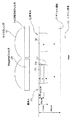
図1は本発明の実施例による固体撮像素子の第1の構成例を示す断面図である。
この図1はシリコン基板10の上層部に設けたPウェル領域12に2種類の画素A20、画素B30が形成された状態を示している。なお、各画素A、Bは図示しないチャネルストップ領域によって相互に分離され、また、素子全体としては2次元アレイ状に配列されて2次元エリアセンサを構成している。
一方の画素Aの光電変換部は、Pウェル領域12に下層から上層に向けてN層22、P層24、N層26を設けたものであり、Pウェル領域12と合わせて2つのPN接合部を有する構造である。
また、他方の画素Bの光電変換部は、Pウェル領域12にN層32を設けたものであり、Pウェル領域12との間に1つのPN接合部を有する構造である。
なお、図示のように、各層の深さは、Pウェル領域12の4.0μmに対し、各画素A、Nの光電変換部では、N層22の深さが1.1μm、P層24の深さが0.8μm、N層26の深さが0.3μmとなっている。これらはブルー光とレッド光の各波長に対する感光特性に合わせて形成されている。また、画素Bの光電変換部では、N層32の深さが1.1μmとなっている。
FIG. 1 is a cross-sectional view showing a first configuration example of a solid-state imaging device according to an embodiment of the present invention.
FIG. 1 shows a state in which two types of pixels A20 and B30 are formed in a P well region 12 provided in an upper layer portion of a
The photoelectric conversion unit of one pixel A is provided with an
The photoelectric conversion unit of the other pixel B has a structure in which an
As shown in the figure, the depth of each layer is 4.0 μm in the P well region 12, whereas in the photoelectric conversion portion of each pixel A and N, the depth of the
また、画素A20の上部にはマゼンタフィルタ28が配置されており、画素B30の上部にはグリーンフィルタ34が配置されている。したがって、画素A20の光電変換部には、マゼンタフィルタ28によってグリーン光成分を除去した光が入射され、画素B30の光電変換部には、グリーンフィルタ34によってグリーン光成分が入射される。なお、色フィルタ28、34の上には、マイクロレンズ40が配置されており、各画素毎に入射光を集める構造となっている。
また、図では省略しているが、各画素内の各PN接合部に対応して転送ゲートが設けられ、それぞれのPN接合部で生成された信号電荷が所定のタイミングで個別に取り出されるようになっている。
A
Although omitted in the figure, a transfer gate is provided corresponding to each PN junction in each pixel so that signal charges generated at each PN junction can be individually taken out at a predetermined timing. It has become.
このような構成において、画素A20では、マゼンタフィルタ28によってグリーン光成分を除去した光が光電変換部に入射され、基板表面側のP層24とN層26とのPN接合部からはブルー光の信号電荷が生成され、基板裏面側のPウェル領域12とN層22とのPN接合部からはレッド光の信号電荷が生成され、これらの信号電荷は個別に読み出されてブルー信号及びレッド信号に変換されて出力される。
また、画素B30では、グリーンフィルタ34によってグリーン光成分が光電変換部に入射され、Pウェル領域12とN層32とのPN接合部からはグリーン光の信号電荷が生成され、グリーン信号に変換されて出力される。
In such a configuration, in the pixel A20, light from which the green light component has been removed by the
In the pixel B30, a green light component is incident on the photoelectric conversion unit by the green filter 34, and a signal charge of green light is generated from the PN junction between the P well region 12 and the
図2は本発明の実施例による固体撮像素子の第2の構成例を示す断面図である。なお、図1と共通の構成については同一符号を付している。
この例は画素B50の光電変換部を画素A20と同様に、下層から上層に向けてN層52、P層54、N層56の3層構造とし、Pウェル領域12と合わせて2つのPN接合部を有する構造としたものである。なお、各層の深さは画素A20と同様となっている。この画素B50では、2つのPN接合部を用いてグリーン光の信号電荷が生成され、1つのグリーン信号に加算されて出力される。なお、2つのグリーン信号を色信号と輝度信号に別々に利用してもよい。
本例では、各画素A、Bの構造を作り分ける必要がなくなり、作成が容易となる利点がある。
FIG. 2 is a cross-sectional view showing a second configuration example of the solid-state imaging device according to the embodiment of the present invention. In addition, the same code | symbol is attached | subjected about the same structure as FIG.
In this example, similarly to the pixel A20, the photoelectric conversion unit of the pixel B50 has a three-layer structure of an
In this example, there is an advantage that it is not necessary to make the structure of each pixel A and B separately, and the creation is easy.
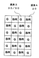
図3〜図6は本実施例で用いることができる画素配列の具体例を示す平面図である。
図3は画素A20(B/R)と画素B30または50(G)を対角線方向に連続して配置し、縦方向及び横方向に交互に配置したものである。従来のモザイク配列では、RとBがGに対し、それぞれ半分の数しか取れないのに対し、図3の例では、倍の数が取れるので、色解像度が向上する利点がある。
図4は画素A20(B/R)の縦1列と画素B30または50(G)の縦1列とを交互に配置したものである。従来のRGBの3列パターンでは、3画素繰り返しとなるが、図4の例では、2画素繰り返しとなり、色の解像度が向上する利点がある。
図5は画素A20(B/R)の縦1列と画素B30または50(G)の縦2列とを交互に配置したものである。従来のRGBの3列パターンでは、グリーン信号が輝度信号に用いられるが、図5の例では、3画素中にグリーンの画素が2つ存在するため、1つのグリーン画素を輝度信号用に用いても、残りのグリーン画素の信号を隣接するRとBの画素の信号に合成することにより、解像度を落とすことなく、2倍の感度を得ることが可能となる。
図6は画素B30または50(G)の列を1列おきに配置するとともに、その中間の列に画素A20(B/R)と画素B30または50を1画素おきに交互に配置したものである。このような配置では、色作成に必要なRとBのサンプリング数が従来と同じ数であるため色解像度は劣化せず、また、グリーン画素が従来の倍となり、解像度がほぼ2倍と高くなる利点がある。また、解像度を従来並みとしてGを加算すれば、その分、感度が高くなる。
3 to 6 are plan views showing specific examples of pixel arrays that can be used in this embodiment.
In FIG. 3, the pixel A20 (B / R) and the pixel B30 or 50 (G) are continuously arranged in the diagonal direction, and alternately arranged in the vertical direction and the horizontal direction. In the conventional mosaic arrangement, R and B can only take half of each of G, whereas the example of FIG. 3 has the advantage of improving the color resolution because it can take twice as many.
In FIG. 4, one vertical column of pixels A20 (B / R) and one vertical column of pixels B30 or 50 (G) are alternately arranged. In the conventional RGB three-row pattern, 3 pixels are repeated, but in the example of FIG. 4, 2 pixels are repeated, and there is an advantage that the color resolution is improved.
FIG. 5 shows an arrangement in which one vertical column of pixels A20 (B / R) and two vertical columns of pixels B30 or 50 (G) are alternately arranged. In the conventional RGB three-row pattern, the green signal is used for the luminance signal, but in the example of FIG. 5, there are two green pixels in the three pixels, so one green pixel is used for the luminance signal. However, by combining the signals of the remaining green pixels with the signals of the adjacent R and B pixels, it is possible to obtain twice the sensitivity without reducing the resolution.
In FIG. 6, every other column of pixels B30 or 50 (G) is arranged, and in the middle column, pixels A20 (B / R) and pixels B30 or 50 are alternately arranged every other pixel. . In such an arrangement, the number of R and B samples necessary for color creation is the same as the conventional number, so the color resolution does not deteriorate, and the green pixel is doubled compared to the conventional one, and the resolution is almost doubled. There are advantages. Moreover, if G is added with the same resolution as before, the sensitivity is increased accordingly.
図7はマゼンタフィルタとグリーンフィルタの分光特性を示している。図示のように、MGで示すマゼンタフィルタはグリーン光成分を除去した成分光を透過し、逆にGで示すグリーンフィルタはグリーン光成分を透過する。
図8は図1に示した画素配列例におけるRGB信号の出力特性を示しており、図9は図2に示した画素配列例におけるRGB信号の出力特性を示している。
すなわち、図2に示すような、下地の異なるバルク構造を配置することで、1つのグリーンフィルタの下で異なるグリーン信号G1とG2を得ることができる。
FIG. 7 shows the spectral characteristics of the magenta filter and the green filter. As shown in the figure, the magenta filter indicated by MG transmits the component light from which the green light component is removed, and conversely, the green filter indicated by G transmits the green light component.
FIG. 8 shows output characteristics of the RGB signals in the pixel array example shown in FIG. 1, and FIG. 9 shows output characteristics of the RGB signals in the pixel array example shown in FIG.
That is, as shown in FIG. 2, different green signals G1 and G2 can be obtained under one green filter by arranging bulk structures with different bases.
10……シリコン基板、12……Pウェル領域、20……画素A、28……マゼンタフィルタ、30、50……画素B、34……グリーンフィルタ、40……マイクロレンズ。
DESCRIPTION OF
Claims (5)
少なくとも1つのPN接合部を設けた光電変換部を含む画素Bと、
前記画素A上に配置される第1の色フィルタと、
前記画素B上に配置される第2の色フィルタと、
前記画素Aの2つのPN接合部から第1の色信号及び第2の色信号を検出し、前記画素BのPN接合部から第3の色信号を検出する検出手段と、
を有することを特徴とする固体撮像素子。 A pixel A including a photoelectric conversion unit provided with at least two PN junctions in the depth direction of the semiconductor substrate;
A pixel B including a photoelectric conversion unit provided with at least one PN junction;
A first color filter disposed on the pixel A;
A second color filter disposed on the pixel B;
Detecting means for detecting a first color signal and a second color signal from the two PN junctions of the pixel A, and detecting a third color signal from the PN junction of the pixel B;
A solid-state imaging device comprising:
The first color filter is a magenta filter, the second filter is a blue filter, the first color signal is a blue signal, the second color signal is a red signal, and the third color signal is The solid-state imaging device according to claim 1, wherein the color signal is a green signal.
Priority Applications (3)
| Application Number | Priority Date | Filing Date | Title |
|---|---|---|---|
| JP2004356204A JP2006165362A (en) | 2004-12-09 | 2004-12-09 | Solid-state imaging element |
| US11/298,063 US7714915B2 (en) | 2004-12-09 | 2005-12-09 | Solid-state image device having multiple PN junctions in a depth direction, each of which provides and output signal |
| US12/771,925 US8253830B2 (en) | 2004-12-09 | 2010-04-30 | Solid state image device having multiple PN junctions in a depth direction, each of which provides an output signal |
Applications Claiming Priority (1)
| Application Number | Priority Date | Filing Date | Title |
|---|---|---|---|
| JP2004356204A JP2006165362A (en) | 2004-12-09 | 2004-12-09 | Solid-state imaging element |
Publications (1)
| Publication Number | Publication Date |
|---|---|
| JP2006165362A true JP2006165362A (en) | 2006-06-22 |
Family
ID=36667025
Family Applications (1)
| Application Number | Title | Priority Date | Filing Date |
|---|---|---|---|
| JP2004356204A Pending JP2006165362A (en) | 2004-12-09 | 2004-12-09 | Solid-state imaging element |
Country Status (2)
| Country | Link |
|---|---|
| US (2) | US7714915B2 (en) |
| JP (1) | JP2006165362A (en) |
Cited By (8)
| Publication number | Priority date | Publication date | Assignee | Title |
|---|---|---|---|---|
| JP2008072098A (en) * | 2006-08-17 | 2008-03-27 | Sony Corp | Semiconductor image sensor |
| WO2010004683A1 (en) * | 2008-07-11 | 2010-01-14 | パナソニック株式会社 | Solid-state imaging device |
| US8400538B2 (en) | 2007-04-23 | 2013-03-19 | Samsung Electronics Co., Ltd. | Apparatus and method for capturing images |
| US8436308B2 (en) | 2008-05-09 | 2013-05-07 | Samsung Electronics Co., Ltd. | Multilayer image sensor |
| JP5196488B2 (en) * | 2006-07-21 | 2013-05-15 | ルネサスエレクトロニクス株式会社 | Photoelectric conversion device and imaging device |
| US9337231B2 (en) | 2009-08-08 | 2016-05-10 | Nikon Corporation | Solid state image sensor with plural overlapping photoelectric conversion units |
| JP2017063198A (en) * | 2015-09-25 | 2017-03-30 | 三星電子株式会社Samsung Electronics Co.,Ltd. | Image sensor including color separation element, and imaging device including image sensor |
| KR20170041089A (en) * | 2015-10-06 | 2017-04-14 | 삼성전자주식회사 | Image sensor including color separation element |
Families Citing this family (9)
| Publication number | Priority date | Publication date | Assignee | Title |
|---|---|---|---|---|
| KR100982685B1 (en) * | 2005-10-13 | 2010-09-17 | 알제이에스 테크놀로지, 인코포레이티드 | System and method for a high performance color filter mosaic array |
| US20080055436A1 (en) * | 2006-08-29 | 2008-03-06 | Atif Sarwari | Method, imager and system providing paired-bayer color filter array and interlaced readout |
| CN101345248B (en) * | 2007-07-09 | 2010-07-14 | 博立码杰通讯(深圳)有限公司 | Multi-optical spectrum light-sensitive device and preparation thereof |
| EP2133918B1 (en) * | 2008-06-09 | 2015-01-28 | Sony Corporation | Solid-state imaging device, drive method thereof and electronic apparatus |
| US20110317048A1 (en) * | 2010-06-29 | 2011-12-29 | Aptina Imaging Corporation | Image sensor with dual layer photodiode structure |
| US8582006B2 (en) * | 2011-01-21 | 2013-11-12 | Aptina Imaging Corporation | Pixel arrangement for extended dynamic range imaging |
| JP2013239634A (en) * | 2012-05-16 | 2013-11-28 | Toshiba Corp | Solid-state imaging device |
| KR102114343B1 (en) | 2013-11-06 | 2020-05-22 | 삼성전자주식회사 | Sensing Pixel and Image Sensor including Thereof |
| CN112770020A (en) * | 2019-11-05 | 2021-05-07 | 北京小米移动软件有限公司 | Image sensing module, method, device, electronic device and medium |
Citations (3)
| Publication number | Priority date | Publication date | Assignee | Title |
|---|---|---|---|---|
| JP2004165242A (en) * | 2002-11-11 | 2004-06-10 | Canon Inc | Color imaging device and color light receiving element |
| JP2004273952A (en) * | 2003-03-11 | 2004-09-30 | Fuji Film Microdevices Co Ltd | Ccd solid-state color image pickup device |
| JP2004281773A (en) * | 2003-03-17 | 2004-10-07 | Fuji Film Microdevices Co Ltd | Mos type color solid-state imaging device |
Family Cites Families (14)
| Publication number | Priority date | Publication date | Assignee | Title |
|---|---|---|---|---|
| JPH0628450B2 (en) * | 1983-01-28 | 1994-04-13 | 松下電器産業株式会社 | Solid-state imaging device |
| US5696875A (en) * | 1995-10-31 | 1997-12-09 | Motorola, Inc. | Method and system for compressing a speech signal using nonlinear prediction |
| JP2000514548A (en) * | 1996-05-10 | 2000-10-31 | アプライド、サイエンス、フィクション、インコーポレーテッド | Luminance priority color sensor |
| JP3830590B2 (en) * | 1996-10-30 | 2006-10-04 | 株式会社東芝 | Solid-state imaging device |
| US5965875A (en) * | 1998-04-24 | 1999-10-12 | Foveon, Inc. | Color separation in an active pixel cell imaging array using a triple-well structure |
| US6482669B1 (en) * | 2001-05-30 | 2002-11-19 | Taiwan Semiconductor Manufacturing Company | Colors only process to reduce package yield loss |
| JP2003298038A (en) * | 2002-04-05 | 2003-10-17 | Canon Inc | Photoelectric conversion element and solid-state imaging device using the same |
| US7129466B2 (en) * | 2002-05-08 | 2006-10-31 | Canon Kabushiki Kaisha | Color image pickup device and color light-receiving device |
| US7008814B2 (en) * | 2002-08-23 | 2006-03-07 | Motorola, Inc. | Method and apparatus for increasing digital color imaging utilizing tandem RGB photodiodes |
| US7554587B2 (en) * | 2003-03-11 | 2009-06-30 | Fujifilm Corporation | Color solid-state image pickup device |
| JP4388752B2 (en) * | 2003-03-11 | 2009-12-24 | 富士フイルム株式会社 | CCD color solid-state imaging device |
| US20050030398A1 (en) * | 2003-08-07 | 2005-02-10 | Eastman Kodak Company | Hybrid two color per pixel architecture using both color filter materials and wavelength dependent silicon absorption |
| JP4324502B2 (en) * | 2004-03-29 | 2009-09-02 | 富士フイルム株式会社 | CCD solid-state image sensor and digital camera |
| JP4507769B2 (en) * | 2004-08-31 | 2010-07-21 | ソニー株式会社 | Solid-state image sensor, camera module, and electronic device module |
-
2004
- 2004-12-09 JP JP2004356204A patent/JP2006165362A/en active Pending
-
2005
- 2005-12-09 US US11/298,063 patent/US7714915B2/en not_active Expired - Fee Related
-
2010
- 2010-04-30 US US12/771,925 patent/US8253830B2/en not_active Expired - Fee Related
Patent Citations (3)
| Publication number | Priority date | Publication date | Assignee | Title |
|---|---|---|---|---|
| JP2004165242A (en) * | 2002-11-11 | 2004-06-10 | Canon Inc | Color imaging device and color light receiving element |
| JP2004273952A (en) * | 2003-03-11 | 2004-09-30 | Fuji Film Microdevices Co Ltd | Ccd solid-state color image pickup device |
| JP2004281773A (en) * | 2003-03-17 | 2004-10-07 | Fuji Film Microdevices Co Ltd | Mos type color solid-state imaging device |
Cited By (12)
| Publication number | Priority date | Publication date | Assignee | Title |
|---|---|---|---|---|
| JP5196488B2 (en) * | 2006-07-21 | 2013-05-15 | ルネサスエレクトロニクス株式会社 | Photoelectric conversion device and imaging device |
| JP2008072098A (en) * | 2006-08-17 | 2008-03-27 | Sony Corp | Semiconductor image sensor |
| US8400538B2 (en) | 2007-04-23 | 2013-03-19 | Samsung Electronics Co., Ltd. | Apparatus and method for capturing images |
| US8436308B2 (en) | 2008-05-09 | 2013-05-07 | Samsung Electronics Co., Ltd. | Multilayer image sensor |
| WO2010004683A1 (en) * | 2008-07-11 | 2010-01-14 | パナソニック株式会社 | Solid-state imaging device |
| US8243176B2 (en) | 2008-07-11 | 2012-08-14 | Panasonic Corporation | Solid-state image sensor |
| US9337231B2 (en) | 2009-08-08 | 2016-05-10 | Nikon Corporation | Solid state image sensor with plural overlapping photoelectric conversion units |
| JP2017063198A (en) * | 2015-09-25 | 2017-03-30 | 三星電子株式会社Samsung Electronics Co.,Ltd. | Image sensor including color separation element, and imaging device including image sensor |
| KR20170037452A (en) * | 2015-09-25 | 2017-04-04 | 삼성전자주식회사 | Image sensor including color separation element and image pickup apparatus including the image sensor |
| KR102519178B1 (en) * | 2015-09-25 | 2023-04-06 | 삼성전자주식회사 | Image sensor including color separation element and image pickup apparatus including the image sensor |
| KR20170041089A (en) * | 2015-10-06 | 2017-04-14 | 삼성전자주식회사 | Image sensor including color separation element |
| KR102409389B1 (en) * | 2015-10-06 | 2022-06-15 | 삼성전자주식회사 | Image sensor including color separation element |
Also Published As
| Publication number | Publication date |
|---|---|
| US8253830B2 (en) | 2012-08-28 |
| US20060181623A1 (en) | 2006-08-17 |
| US20100203666A1 (en) | 2010-08-12 |
| US7714915B2 (en) | 2010-05-11 |
Similar Documents
| Publication | Publication Date | Title |
|---|---|---|
| US7714915B2 (en) | Solid-state image device having multiple PN junctions in a depth direction, each of which provides and output signal | |
| US10032810B2 (en) | Image sensor with dual layer photodiode structure | |
| US9596423B1 (en) | Charge summing in an image sensor | |
| KR102614792B1 (en) | Semiconductor device and electronic apparatus | |
| US8243176B2 (en) | Solid-state image sensor | |
| JP4457325B2 (en) | Solid-state imaging device | |
| JP5661201B2 (en) | Solid-state imaging device | |
| JP4599258B2 (en) | Solid-state image sensor | |
| JP5320989B2 (en) | Solid-state imaging device and electronic apparatus | |
| JP4770276B2 (en) | Solid-state imaging device and solid-state imaging device | |
| US8345132B2 (en) | Image sensor with dual element color filter array and three channel color output | |
| KR20080091023A (en) | Solid-state imaging device and imaging apparatus | |
| KR20070120360A (en) | Camera module | |
| JP2006237737A (en) | Color filter array and solid state image sensor | |
| JP2016058818A (en) | Imaging apparatus and imaging system | |
| JP2009088255A (en) | Color solid-state imaging device and electronic information equipment | |
| JP4469732B2 (en) | Solid-state image sensor | |
| JP2007288294A (en) | Solid-state imaging apparatus and camera | |
| KR100837454B1 (en) | Solid-state image sensing device | |
| JP2008072098A (en) | Semiconductor image sensor | |
| JP2009147147A (en) | Organic photoelectric conversion device | |
| JPH1126737A (en) | Solid-state image sensing device | |
| EP2784820A1 (en) | Solid state imaging device | |
| KR20160072508A (en) | Color filter array and image sensor having the same | |
| JP5130614B2 (en) | Semiconductor image sensor |
Legal Events
| Date | Code | Title | Description |
|---|---|---|---|
| A621 | Written request for application examination |
Free format text: JAPANESE INTERMEDIATE CODE: A621 Effective date: 20070824 |
|
| RD02 | Notification of acceptance of power of attorney |
Free format text: JAPANESE INTERMEDIATE CODE: A7422 Effective date: 20090817 |
|
| RD04 | Notification of resignation of power of attorney |
Free format text: JAPANESE INTERMEDIATE CODE: A7424 Effective date: 20091013 |
|
| A977 | Report on retrieval |
Free format text: JAPANESE INTERMEDIATE CODE: A971007 Effective date: 20100722 |
|
| A131 | Notification of reasons for refusal |
Free format text: JAPANESE INTERMEDIATE CODE: A131 Effective date: 20100727 |
|
| A521 | Request for written amendment filed |
Free format text: JAPANESE INTERMEDIATE CODE: A523 Effective date: 20100927 |
|
| A02 | Decision of refusal |
Free format text: JAPANESE INTERMEDIATE CODE: A02 Effective date: 20110705 |