JP2006156716A - Semiconductor device and its manufacturing method - Google Patents
Semiconductor device and its manufacturing method Download PDFInfo
- Publication number
- JP2006156716A JP2006156716A JP2004345349A JP2004345349A JP2006156716A JP 2006156716 A JP2006156716 A JP 2006156716A JP 2004345349 A JP2004345349 A JP 2004345349A JP 2004345349 A JP2004345349 A JP 2004345349A JP 2006156716 A JP2006156716 A JP 2006156716A
- Authority
- JP
- Japan
- Prior art keywords
- film
- wiring layer
- barrier metal
- layer
- tungsten
- Prior art date
- Legal status (The legal status is an assumption and is not a legal conclusion. Google has not performed a legal analysis and makes no representation as to the accuracy of the status listed.)
- Withdrawn
Links
Images


Classifications
-
- H—ELECTRICITY
- H01—ELECTRIC ELEMENTS
- H01L—SEMICONDUCTOR DEVICES NOT COVERED BY CLASS H10
- H01L23/00—Details of semiconductor or other solid state devices
- H01L23/52—Arrangements for conducting electric current within the device in operation from one component to another, i.e. interconnections, e.g. wires, lead frames
- H01L23/522—Arrangements for conducting electric current within the device in operation from one component to another, i.e. interconnections, e.g. wires, lead frames including external interconnections consisting of a multilayer structure of conductive and insulating layers inseparably formed on the semiconductor body
- H01L23/532—Arrangements for conducting electric current within the device in operation from one component to another, i.e. interconnections, e.g. wires, lead frames including external interconnections consisting of a multilayer structure of conductive and insulating layers inseparably formed on the semiconductor body characterised by the materials
- H01L23/53204—Conductive materials
- H01L23/53209—Conductive materials based on metals, e.g. alloys, metal silicides
- H01L23/53214—Conductive materials based on metals, e.g. alloys, metal silicides the principal metal being aluminium
- H01L23/53223—Additional layers associated with aluminium layers, e.g. adhesion, barrier, cladding layers
-
- H—ELECTRICITY
- H01—ELECTRIC ELEMENTS
- H01L—SEMICONDUCTOR DEVICES NOT COVERED BY CLASS H10
- H01L23/00—Details of semiconductor or other solid state devices
- H01L23/52—Arrangements for conducting electric current within the device in operation from one component to another, i.e. interconnections, e.g. wires, lead frames
- H01L23/522—Arrangements for conducting electric current within the device in operation from one component to another, i.e. interconnections, e.g. wires, lead frames including external interconnections consisting of a multilayer structure of conductive and insulating layers inseparably formed on the semiconductor body
- H01L23/5226—Via connections in a multilevel interconnection structure
-
- H—ELECTRICITY
- H01—ELECTRIC ELEMENTS
- H01L—SEMICONDUCTOR DEVICES NOT COVERED BY CLASS H10
- H01L2924/00—Indexing scheme for arrangements or methods for connecting or disconnecting semiconductor or solid-state bodies as covered by H01L24/00
- H01L2924/0001—Technical content checked by a classifier
- H01L2924/0002—Not covered by any one of groups H01L24/00, H01L24/00 and H01L2224/00
Abstract
Description
本発明は半導体装置およびその製造方法に関し、特にアルミ配線層の多層配線構造を有し、アルミ配線層間をタングステンプラグによって電気的に接続する半導体装置およびその製造方法に関する。 The present invention relates to a semiconductor device and a manufacturing method thereof, and more particularly to a semiconductor device having a multilayer wiring structure of aluminum wiring layers and electrically connecting aluminum wiring layers by tungsten plugs and a manufacturing method thereof.
多層配線構造を有する半導体装置として、アルミ配線層間をタングステンプラグによって電気的に接続する構成が知られている。 As a semiconductor device having a multilayer wiring structure, a structure in which aluminum wiring layers are electrically connected by a tungsten plug is known.
多層配線構造とは、半導体基板上に設けた層間絶縁膜を間に挟んで、上下に配線層が配設された構造を上下方向に複数備えた構成である。 The multilayer wiring structure is a configuration in which a plurality of structures in which wiring layers are arranged above and below are provided in the vertical direction with an interlayer insulating film provided on a semiconductor substrate interposed therebetween.
そして、配線層としてはアルミ配線層を使用することが多く、上下のアルミ配線層間を電気的に接続するために、層間絶縁膜を貫通するスルーホール内にタングステン層を充填して形成されたタングステンプラグを使用することが近年行われている。 In many cases, an aluminum wiring layer is used as a wiring layer. In order to electrically connect the upper and lower aluminum wiring layers, tungsten formed by filling a tungsten layer in a through hole penetrating the interlayer insulating film. The use of plugs has been done in recent years.
しかし、近年の半導体装置の微細化に伴い、配線パターンが高密度化しており、層間絶縁膜にスルーホールを設ける際のフォトリソグラフィ工程において、マスク位置合わせのずれに起因して、スルーホールの形成位置が下層の配線層上からずれる、いわゆる「目外れ」が発生することが避けられない事態となってきた。 However, with the recent miniaturization of semiconductor devices, the wiring pattern has become denser, and in the photolithography process when providing a through hole in an interlayer insulating film, the formation of a through hole is caused due to a mask misalignment. It has become unavoidable that a so-called “missing” occurs in which the position shifts from the lower wiring layer.
目外れを防止するには配線幅を広げれば良いが、それは半導体装置の小型化に逆行することになる。 Although it is sufficient to widen the wiring width in order to prevent losing the eye, this goes against the downsizing of the semiconductor device.
また、目外れの防止には、スルーホールを縮小することも有効であるが、配線層との接触面積の減少につながり、接触抵抗が増大するので、これも望ましくない。 Further, it is effective to reduce the size of the through hole in order to prevent the disconnection, but this leads to a decrease in the contact area with the wiring layer and increases the contact resistance, which is also undesirable.
このように、配線パターンが高密度化した半導体装置においては、目外れの発生を避けることが困難であり、最近では逆に、目外れを許容する設計も実行されつつある。 As described above, in a semiconductor device having a high wiring pattern density, it is difficult to avoid the occurrence of an off-line, and conversely, on the contrary, a design that allows the off-line is being carried out.
すなわち、半導体装置の設計において、例えば、フォトリソグラフィ工程におけるマスク位置合わせマージンを小さくし、制御された範囲で目外れが起きる可能性を高める設計を行う。ここで、制御された範囲とは、目外れが起きた場合でも、スルーホールが完全に配線層上から外れることはなく、少なくとも一部が配線層上に位置するようにマスク位置合わせマージンを設定することを意味する。 That is, in designing a semiconductor device, for example, a mask alignment margin in a photolithography process is reduced, and a design is performed to increase the possibility of occurrence of off-axis in a controlled range. Here, the controlled range means that the mask alignment margin is set so that the through-holes are not completely removed from the wiring layer even if they are missed, and at least part of them are located on the wiring layer. It means to do.
このような制御された範囲での目外れが起きると、スルーホールの底面の一部に配線層の上面が露出し、スルーホールの側面に配線層の側面が露出することになり、そこにタングステン層を充填すると、配線層とタングステン層との接触面積を目外れが起きない場合と、同等かそれ以上に確保することが可能となる。 When such a controlled deviation occurs, the top surface of the wiring layer is exposed at a part of the bottom surface of the through hole, and the side surface of the wiring layer is exposed at the side surface of the through hole. When the layer is filled, the contact area between the wiring layer and the tungsten layer can be ensured to be equal to or higher than that in the case where no disconnection occurs.
ここで、配線層としてアルミ配線層を使用し、タングステンプラグにより配線層間の電気的接続を行う場合、例えば、特許文献1で示されるように、スルーホール内面(側面および底面を含む)にチタン膜と窒化チタン膜との2層構造のバリアメタル層を形成することが従来的に行われている。
Here, when an aluminum wiring layer is used as the wiring layer and electrical connection between the wiring layers is performed by a tungsten plug, for example, as shown in
特許文献1では、チタン膜および窒化チタン膜の形成にスパッタリング法を使用することが開示されているが、スパッタリング法では、スルーホールのアスペクト比が2以上になると、スルーホールの底面にはバリアメタル層を形成できるものの、側面にはバリアメタル層が形成されにくいとされている。
このことは、スルーホールの目外れが発生した場合に、スルーホールの側面に露出する配線層の側面上にバリアメタル層が形成されない可能性が高くなることを意味している。 This means that when the through hole is disconnected, there is a high possibility that the barrier metal layer is not formed on the side surface of the wiring layer exposed on the side surface of the through hole.
ここで、スルーホール内に充填されるタングステン膜はCVD(chemical vapor deposition)で形成されるが、バリアメタル層が形成されない状態でタングステン膜の形成を行うと、タングステン膜の形成に使用される六フッ化タングステン(WF6)と配線層のアルミニウムとが反応し、フッ化アルミニウム(AlF3)が生成され、ボイドが発生する原因となる。ボイドが発生すると、タングステンプラグとアルミ配線層との電気的接続の信頼性の低下や、接触抵抗の増加を引き起こすことが特許文献1に記載されている。
Here, the tungsten film filled in the through hole is formed by chemical vapor deposition (CVD). However, if the tungsten film is formed in a state where the barrier metal layer is not formed, the tungsten film used for forming the tungsten film is formed. Tungsten fluoride (WF 6 ) reacts with aluminum in the wiring layer to produce aluminum fluoride (AlF 3 ), which causes voids.
また、非特許文献1には、フッ素(F)はチタンと反応しやすく、フッ化チタン(TiF3、TiF4)が生成されると、チタン膜と窒化チタン膜との接着力が低下して剥離を起こしやすいことが報告されている。
In
以上説明したように、従来の半導体装置においては、スルーホール内にバリアメタル層が形成されない部分が存在する可能性を有し、当該部分に起因して、タングステンプラグとアルミ配線層との電気的接続の信頼性の低下や、接触抵抗の増加を引き起こすという問題があった。 As described above, in the conventional semiconductor device, there is a possibility that a part where the barrier metal layer is not formed exists in the through hole, and the electrical connection between the tungsten plug and the aluminum wiring layer is caused by the part. There has been a problem that the reliability of the connection is lowered and the contact resistance is increased.
本発明は上記のような問題点を解消するためになされたもので、アルミ配線層間をタングステンプラグによって電気的に接続する構成において、スルーホール内面全面にバリアメタル層が形成され、タングステンプラグとアルミ配線層との電気的接続の信頼性が高く、接触抵抗が低い半導体装置を提供することを目的とする。 The present invention has been made to solve the above-described problems. In a configuration in which aluminum wiring layers are electrically connected by a tungsten plug, a barrier metal layer is formed on the entire inner surface of the through hole. An object of the present invention is to provide a semiconductor device with high reliability of electrical connection with a wiring layer and low contact resistance.
本発明に係る請求項1記載の半導体装置は、多層配線構造を有する半導体装置であって、半導体基板上に配設された多層配線層と、前記多層配線層のうち、アルミ配線層で構成される下層配線層と上層配線層との間に配設された層間絶縁膜と、前記層間絶縁膜を貫通し、前記下層配線層と前記上層配線層とを電気的に接続するコンタクト部と、を備え、前記コンタクト部は、前記層間絶縁膜を貫通して前記下層配線層上に到達するスルーホールと、前記スルーホールの内面に沿って配設されたバリアメタル層と、前記バリアメタル層で規定される前記スルーホール内に充填されたタングステンプラグとを有し、前記バリアメタル層は、アモルファス金属膜を含んでいる。 According to a first aspect of the present invention, there is provided a semiconductor device having a multilayer wiring structure, comprising: a multilayer wiring layer disposed on a semiconductor substrate; and an aluminum wiring layer among the multilayer wiring layers. An interlayer insulating film disposed between the lower wiring layer and the upper wiring layer, and a contact portion that penetrates the interlayer insulating film and electrically connects the lower wiring layer and the upper wiring layer. The contact portion is defined by a through hole that penetrates the interlayer insulating film and reaches the lower wiring layer, a barrier metal layer disposed along an inner surface of the through hole, and the barrier metal layer A tungsten plug filled in the through hole, and the barrier metal layer includes an amorphous metal film.
本発明に係る請求項7記載の半導体装置の製造方法は、半導体基板上に配設された多層配線層と、前記多層配線層のうち、アルミ配線層で構成される下層配線層と上層配線層との間に配設された層間絶縁膜と、前記層間絶縁膜を貫通し、前記下層配線層と前記上層配線層とを電気的に接続するコンタクト部とを備えた多層配線構造を有する半導体装置の製造方法であって、前記下層配線層を覆うように前記層間絶縁膜を形成する工程(a)と、前記層間絶縁膜を貫通して前記下層配線層上に到達するスルーホールを形成する工程(b)と、前記スルーホールの内面に沿うようにバリアメタル層を形成する工程(c)と、前記バリアメタル層で規定される前記スルーホール内にタングステンプラグを形成する工程(d)と、前記タングステンプラグに接続されるように、前記層間絶縁膜上に前記上層配線層を形成する工程(e)とを備え、前記工程(c)は、DCマグネトロンスパッタを用いて前記金属バリアメタル層の金属材料をスパッタリングしてスパッタ粒子を生成するとともに、前記半導体基板に高周波電圧をバイアスして、前記スパッタ粒子を前記半導体基板に引きつけることで前記バリアメタル層を形成する工程を含み、前記DCマグネトロンスパッタのDCパワーは1〜40kW、成膜温度は室温〜400℃とし、前記半導体基板に与える高周波のパワーは1kW以下とし、前記工程(d)は、前記バリアメタル層で規定される前記スルーホール内にCVDによりタングステン膜を充填する工程を含んでいる。 According to a seventh aspect of the present invention, there is provided a semiconductor device manufacturing method comprising: a multilayer wiring layer disposed on a semiconductor substrate; and a lower wiring layer and an upper wiring layer formed of an aluminum wiring layer among the multilayer wiring layers. Semiconductor device having a multilayer wiring structure comprising an interlayer insulating film disposed between and a contact portion passing through the interlayer insulating film and electrically connecting the lower wiring layer and the upper wiring layer And (a) forming the interlayer insulating film so as to cover the lower wiring layer, and forming a through hole that penetrates the interlayer insulating film and reaches the lower wiring layer (b), a step (c) of forming a barrier metal layer along the inner surface of the through hole, and a step (d) of forming a tungsten plug in the through hole defined by the barrier metal layer, Connected to the tungsten plug The step (e) of forming the upper wiring layer on the interlayer insulating film, wherein the step (c) comprises sputtering the metal material of the metal barrier metal layer using DC magnetron sputtering. The method includes forming sputter particles, biasing a high frequency voltage to the semiconductor substrate, and forming the barrier metal layer by attracting the sputter particles to the semiconductor substrate, and the DC power of the DC magnetron sputter is 1 to 40 kW, the film formation temperature is room temperature to 400 ° C., the high frequency power applied to the semiconductor substrate is 1 kW or less, and the step (d) forms a tungsten film by CVD in the through hole defined by the barrier metal layer. Filling.
本発明に係る請求項1記載の半導体装置によれば、スルーホールの内面に沿って配設されたバリアメタル層がアモルファス金属膜を含むので、タングステンプラグの形成にCVDを使用する場合、発生するWF6やフッ素の拡散がアモルファス金属膜によって防止され、下層配線層のアルミニウムと反応してAlF3が生成されることが防止されるので、下層配線層とタングステンプラグとの電気的接続の信頼性が高く、接触抵抗を低く保つことができる。 According to the semiconductor device of the first aspect of the present invention, the barrier metal layer disposed along the inner surface of the through hole includes the amorphous metal film. Therefore, it is generated when CVD is used for forming the tungsten plug. The diffusion of WF 6 and fluorine is prevented by the amorphous metal film, and the generation of AlF 3 by reaction with aluminum in the lower wiring layer is prevented, so the reliability of the electrical connection between the lower wiring layer and the tungsten plug Is high and the contact resistance can be kept low.
本発明に係る請求項7記載の半導体装置の製造方法によれば、バリアメタル層の形成に際して、DCマグネトロンスパッタを用いて金属バリアメタル層の金属材料をスパッタリングしてスパッタ粒子を生成するとともに、半導体基板に高周波電圧をバイアスして、スパッタ粒子を半導体基板に引きつけるので、バリアメタル層をアモルファス金属膜にすることができるとともに、スルーホールのアスペクト比が大きい場合でもスルーホールの側面にも均一に形成することができる。従って、タングステンプラグの形成時に発生するWF6やフッ素の拡散がアモルファス金属膜によって防止され、下層配線層のアルミニウムと反応してAlF3が生成されることが防止されるので、下層配線層とタングステンプラグとの電気的接続の信頼性が高く、接触抵抗が低い半導体装置を得ることができる。
According to the method for manufacturing a semiconductor device according to
<実施の形態>
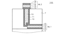
本発明の実施の形態について、図1〜図7を用いて説明する。なお、図1〜図7は製造工程を順に示す断面図であり、最終工程を説明する図7において示される構成が、本発明に係る半導体装置100の発明関連部分を示している。
<Embodiment>
Embodiments of the present invention will be described with reference to FIGS. 1 to 7 are cross-sectional views sequentially showing the manufacturing process, and the configuration shown in FIG. 7 for explaining the final process indicates an invention-related part of the
以下、図1〜図7を参照して半導体装置100の製造方法を説明しつつ、本発明の特徴について説明する。
図1に示す工程において、図示しない半導体基板上にトランジスタ等の半導体素子を形成した後、当該半導体基板および半導体素子を覆うように層間絶縁膜1を形成する。
Hereinafter, features of the present invention will be described while explaining a method of manufacturing the
In the process shown in FIG. 1, after forming a semiconductor element such as a transistor on a semiconductor substrate (not shown), an interlayer
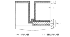
そして、層間絶縁膜1上にスパッタリング法で、チタン膜2、窒化チタン膜3、アルミニウムを主成分とした銅との合金膜等で構成されるアルミニウム膜4、チタン膜5および窒化チタン膜6を順次成膜して多層金属膜を形成した後、その上にフォトリソグラフィ工程で所望の配線パターンを有するレジストマスク(図示せず)を形成する。
Then, an aluminum film 4, a titanium film 5, and a titanium nitride film 6 made of a
その後、当該レジスト膜を用いて、ドライエッチングにより多層金属膜をパターニングすることでアルミ配線層WL1を得る。なお、アルミ配線層WL1を下層配線層と呼称する場合もある。 Thereafter, using the resist film, the multilayer metal film is patterned by dry etching to obtain the aluminum wiring layer WL1. The aluminum wiring layer WL1 may be referred to as a lower wiring layer.
アルミ配線層WL1を形成した後、アルミ配線層WL1上および層間絶縁膜1上を覆うように層間絶縁膜7を形成する。
After forming the aluminum wiring layer WL1, an
次に、図2に示す工程において、層間絶縁膜7上にレジスト材を塗布し、フォトリソグラフィ工程を経て、所定のスルーホールパターンを有するレジストマスクRM1を形成する。
Next, in a process shown in FIG. 2, a resist material is applied on the
そして、当該レジストマスクRM1を用いてドライエッチングにより層間絶縁膜7を選択的にエッチングすることでスルーホール9を形成する。
Then, the through hole 9 is formed by selectively etching the
ここで、レジストマスクRM1の形成に際しては、露光マスクの位置合わせマージンが小さく設定され、制御された範囲でスルーホール9の形成位置がアルミ配線層WL1上からずれる、いわゆる「目外れ」が起きやすいようになっている。 Here, when the resist mask RM1 is formed, the exposure mask alignment margin is set to be small, and the formation position of the through hole 9 is easily shifted from the aluminum wiring layer WL1 within a controlled range, so-called “missing” is likely to occur. It is like that.
従って、図2に示されるように、スルーホール9の底面位置がアルミ配線層WL1上からずれ、スルーホール9の底面の一部に窒化チタン膜6の上面が露出し、スルーホール9の側面の一部に窒化チタン膜6、チタン膜5およびアルミニウム膜4の側面が露出している。なお、アルミ配線層WL1の側面が露出している部分をスリット部と呼称する場合もある。 Therefore, as shown in FIG. 2, the bottom surface position of the through hole 9 is shifted from the aluminum wiring layer WL <b> 1, and the top surface of the titanium nitride film 6 is exposed at a part of the bottom surface of the through hole 9. The side surfaces of the titanium nitride film 6, the titanium film 5, and the aluminum film 4 are partially exposed. A portion where the side surface of the aluminum wiring layer WL1 is exposed may be referred to as a slit portion.
次に、レジストマスクRM1をアッシングによって除去した後、図3に示す工程において、スルーホール9の内面にチタン膜10および窒化チタン膜11の2層構造で構成されるバリアメタル層を形成する。なお、チタン膜10および窒化チタン膜11は、層間絶縁膜7の主面上にも形成される。
Next, after removing the resist mask RM1 by ashing, a barrier metal layer composed of a two-layer structure of a
このバリアメタル層の形成に際しては、チタンターゲットを用いた高指向性スパッタリングが可能で、かつ、高周波電圧を半導体基板にバイアスする基板バイアス機構を備え、チタンターゲットからのスパッタ粒子を半導体基板に引き付けることが可能な成膜装置を用いる。 When forming this barrier metal layer, high directivity sputtering using a titanium target is possible, and a substrate bias mechanism for biasing a high frequency voltage to the semiconductor substrate is provided, and the sputtered particles from the titanium target are attracted to the semiconductor substrate. A film forming apparatus capable of performing the above is used.
ここで、チタンターゲットのスパッタリングには、DCマグネトロンスパッタを用いる。 Here, DC magnetron sputtering is used for sputtering the titanium target.
DCマグネトロンスパッタは、金属ターゲットに印加されるDC(直流)電圧と、金属ターゲットに平行に形成される磁場とで電子にE×Bドリフトを発生させて、高密度のプラズマを生成し、プラズマ中のイオンによって金属ターゲットをスパッタする構成となっている。 In DC magnetron sputtering, a DC (direct current) voltage applied to a metal target and a magnetic field formed in parallel with the metal target generate E × B drift in the electrons to generate a high-density plasma. The metal target is sputtered by the ions.
このようなDCマグネトロンスパッタを用いた高指向性スパッタリングを行うとともに、高周波電圧を半導体基板に印加してバイアスを与え、スパッタ粒子を半導体基板に積極的に引き付けることで窒化チタン膜11をアモルファス金属膜とすることが本発明の特徴の1つである。
In addition to performing highly directional sputtering using such DC magnetron sputtering, a bias is applied by applying a high-frequency voltage to the semiconductor substrate, and the sputtered particles are actively attracted to the semiconductor substrate, thereby forming the
すなわち、高指向性スパッタリングを用いてバリアメタル層を形成する従来の方法では、スルーホールのアスペクト比が2以上となった場合には、スルーホールの側面にバリアメタル層を形成しにくく、特に、スルーホールの目外れが発生した場合には、スリット部(配線層の側面が露出している部分)に均一にバリアメタル層を形成することが難しかった。 That is, in the conventional method of forming the barrier metal layer using highly directional sputtering, when the through hole has an aspect ratio of 2 or more, it is difficult to form the barrier metal layer on the side surface of the through hole. When the through hole is missed, it is difficult to uniformly form the barrier metal layer in the slit portion (the portion where the side surface of the wiring layer is exposed).
また、スリット部にバリアメタル層を形成できたとしても、窒化チタン膜は結晶性の膜であり、タングステン膜の形成に使用される六フッ化タングステン(WF6)が結晶粒界に沿って拡散し、フッ素(F)がアルミ配線層と反応するという問題があった。 Even if the barrier metal layer can be formed in the slit portion, the titanium nitride film is a crystalline film, and tungsten hexafluoride (WF 6 ) used for forming the tungsten film is diffused along the crystal grain boundary. However, there is a problem that fluorine (F) reacts with the aluminum wiring layer.
しかし、アモルファスである窒化チタン膜11は、結晶粒界を有さないので、WF6やフッ素の拡散防止膜として機能する。また、本願が対象とする半導体装置では、スルーホール9のアスペクト比が4以上となる場合があるが、スパッタ粒子を半導体基板に積極的に引き付けて形成される窒化チタン膜11やチタン膜10は、スルーホール9のアスペクト比が大きい場合でもスルーホール9の側面にも均一に形成され、スルーホール9の目外れが発生した場合でも、スリット部に均一にバリアメタル層を形成することが可能である。
However, the amorphous
従って、後のタングステンプラグの形成時に、WF6やフッ素がアルミ配線層WL1のアルミニウムと反応してAlF3が生成されることが防止され、アルミ配線層WL1と後に形成されるタングステンプラグとの電気的接続の信頼性の低下や、接触抵抗の増加を防止できる。 Accordingly, during the subsequent formation of the tungsten plug, it is possible to prevent WF 6 and fluorine from reacting with the aluminum of the aluminum wiring layer WL1 to generate AlF 3, and the electrical connection between the aluminum wiring layer WL1 and the tungsten plug to be formed later is prevented. It is possible to prevent a decrease in reliability of connection and an increase in contact resistance.
また、フッ素はチタンと反応しやすいが、アモルファスである窒化チタン膜11がチタン膜10上を覆っているので、フッ素が拡散してチタン膜10に到達することが防止され、チタン膜10と窒化チタン膜11との接着力が低下して剥離することが防止される。
In addition, although fluorine easily reacts with titanium, since the amorphous
ここで、チタン膜10および窒化チタン膜11の形成条件の一例を説明する。
金属ターゲットとしてチタンターゲットを用い、DCマグネトロンスパッタのDCパワーとして1〜40kWとする。また、半導体基板に与える高周波のパワーは0〜1kWとし、半導体基板を搭載するステージの温度、すなわち成膜温度は室温〜400℃とする。なお、高周波のパワーが0である場合はスパッタ粒子を半導体基板に積極的に引き付けるという効果は期待できないが、限りなく0に近いパワーを印加する場合もあり得るので、上記範囲を開示している。なお、上記パラメータの例示した範囲内での組み合わせによりチタン膜10および/または窒化チタン膜11をアモルファスにすることができる。
Here, an example of conditions for forming the
A titanium target is used as the metal target, and the DC power of DC magnetron sputtering is 1 to 40 kW. The high frequency power applied to the semiconductor substrate is 0 to 1 kW, and the temperature of the stage on which the semiconductor substrate is mounted, that is, the film formation temperature is room temperature to 400 ° C. When the high frequency power is 0, the effect of positively attracting the sputtered particles to the semiconductor substrate cannot be expected. However, since the power close to 0 may be applied, the above range is disclosed. . Note that the
上記条件下において、チタン膜10の形成に際しては、一旦、真空状態にしたプロセス室内にアルゴンガスを導入し、プロセス室内の圧力を0.4〜1.0Pa(パスカル)の範囲で制御して、半導体基板上の膜厚の均一性が最も良好になる条件を選択する。
Under the above conditions, when forming the
また、窒化チタン膜11の形成に際しては、プロセス室内に窒素とアルゴンの混合ガスを導入し、プロセス室内の圧力を0.4〜1.0Paの範囲で制御する。このとき、窒素の流量は、混合ガスの流量の50%以上となるように制御を行い、半導体基板上の膜厚の均一性が最も良好になる条件を選択する。
Further, when the
なお、上記条件では、チタン膜10も半導体基板に高周波バイアスを与えて形成するのでアモルファスとなるが、チタン膜10は必ずしもアモルファスでなくても良い。
Under the above conditions, the
また、上述したように、本願では金属元素の供給にDCマグネトロンスパッタを用いており、物理的堆積法いわゆるPVD(physical vapor deposition)により金属膜の成膜を行っているが、PVDを用いることは他の方法を使用する場合に比べて以下の点で有利である。 In addition, as described above, in the present application, DC magnetron sputtering is used for supplying a metal element, and a metal film is formed by a physical deposition method, so-called PVD (physical vapor deposition), but PVD is used. Compared to the use of other methods, there are advantages in the following points.
すなわち、CVDによりスルーホール内に窒化チタン膜を形成する場合、TiCl4-TiNを原料ガスとして用いるが、この場合の成膜温度は600℃以上となるため、アルミ配線層に係合するスルーホールの内面に窒化チタン膜を形成するには不適当である。しかし、上述したPVDであれば、ステージの温度、室温〜400℃の範囲であるので、アルミ配線層WL1に影響を与えることはない。 That is, when a titanium nitride film is formed in a through hole by CVD, TiCl 4 —TiN is used as a source gas. In this case, the film forming temperature is 600 ° C. or more, and therefore the through hole engaged with the aluminum wiring layer is used. It is inappropriate to form a titanium nitride film on the inner surface of the film. However, with the PVD described above, the temperature of the stage is in the range of room temperature to 400 ° C., and therefore does not affect the aluminum wiring layer WL1.
また、成膜温度が450℃以下であるTDMAT(tetrakis dimethyl amino titanium)を用いてMOCVD(metal organic CVD)により窒化チタン膜を形成した場合、次にスルーホール内に充填するタングステン膜をCVDにより成膜する際に、MOCVDで形成した窒化チタン膜中に含まれる不純物がガスとして放出され、タングステン膜が成長できない。しかし、上述したPVDであれば、窒化チタン膜11中には不純物を含まず、タングステン膜の成膜に支障を来すようなガス放出は起こらない。
In addition, when a titanium nitride film is formed by MOCVD (metal organic CVD) using TDMAT (tetrakis dimethyl amino titanium) having a deposition temperature of 450 ° C. or lower, a tungsten film to be filled in the through hole is formed by CVD. When the film is formed, impurities contained in the titanium nitride film formed by MOCVD are released as a gas, and the tungsten film cannot be grown. However, in the case of the PVD described above, the
なお、窒化チタン膜11は、WF6やフッ素の拡散防止膜として機能するだけでなく、タングステン膜の成膜に際しては成長のためのシード膜としても機能する。
The
ここで、再び、図を用いた製造方法の説明に戻る。
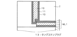
窒化チタン膜11を形成した後、図4に示すようにCVDにより、タングステン膜12を成膜し、スルーホール9内にタングステン膜12する充填する。なお、タングステン膜12は、層間絶縁膜7の主面上にも形成される。
Here, it returns to description of the manufacturing method using a figure again.
After the
その後、CMP(chemical mechanical polishing)により、層間絶縁膜7の主面上のタングステン膜12、窒化チタン膜11およびチタン膜10を除去し、層間絶縁膜7の主面を露出させることで、図5に示すように、スルーホール9内にタングステンプラグ13が埋め込まれた構成を得る。
Thereafter, the
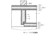
次に、図6に示す工程において、スパッタリング法で、チタン膜14、窒化チタン膜15、アルミニウムと銅の合金膜やアルミニウムの単体膜で構成されるアルミニウム膜16、チタン膜17および窒化チタン膜18を順次成膜して多層金属膜を形成した後、その上にフォトリソグラフィ工程で所望の配線パターンを有するレジストマスクRM2を形成する。
Next, in the step shown in FIG. 6, the
その後、当該レジスト膜RM2を用いて、ドライエッチングにより多層金属膜をパターニングすることで、図7に示すようにタングステンプラグ13に接続されるアルミ配線層WL2を得る。なお、アルミ配線層WL2を上層配線層と呼称する場合もある。なお、スルーホール9、チタン膜10、窒化チタン膜11およびタングステンプラグ13とで、下層配線層と上層配線層とが電気的に接続されるので、この部分をコンタクト部を総称する。
Thereafter, by using the resist film RM2 to pattern the multilayer metal film by dry etching, an aluminum wiring layer WL2 connected to the
以後は、層間絶縁膜7上にさらに層間絶縁膜を形成し、図1〜図7を用いて説明した工程と同様の工程により、アルミ配線層WL2と、それよりもさらに上層のアルミ配線層との電気的接続を行うタングステンプラグを形成するという動作を繰り返すことで、最終的な半導体装置100を得ることになる。なお、半導体装置100には、上述した多層配線層以外にも層間絶縁膜中に形成される構成も含んでおり、多層配線層の形成と併行してそれらの形成が行われるが、それらについては本発明との関係が薄いので、説明は省略する。
Thereafter, an interlayer insulating film is further formed on the
<変形例1>
以上説明した本発明に係る実施の形態では、スルーホール9の内面にチタン膜10および窒化チタン膜11の2層構造で構成されるバリアメタル層を形成する例を示したが、これらの代わりに、図8に示す半導体装置100Aのように、窒化タングステン膜20およびタングステン膜21の2層構造を形成してバリアメタル層としても良い。
<
In the embodiment according to the present invention described above, the example in which the barrier metal layer constituted by the two-layer structure of the
ここで、窒化タングステン膜20およびタングステン膜21は、チタン膜10および窒化チタン膜11と同様にスパッタ粒子を半導体基板に積極的に引き付けることで形成されるので、共にアモルファスとなっている。
Here, since the
そして、アモルファス金属膜である窒化タングステン膜20は、結晶粒界を有さないので、タングステンプラグ形成時に、WF6やフッ素の拡散防止膜として機能し、フッ素がバリアメタル層を通過してアルミ配線層WL1と反応してAlF3が生成されることが防止され、アルミ配線層WL1と後に形成されるタングステンプラグとの電気的接続の信頼性の低下や、接触抵抗の増加を防止できる。
Since the
なお、タングステン膜21は、タングステンプラグ形成時にCVDによるタングステン膜の成長のためのシード膜となりやすいので、タングステン膜21を窒化タングステン膜20上に形成することで、タングステンプラグの成長をよりスムーズに行うことができる。
Since the
ここで、窒化タングステン膜20およびタングステン膜21の形成条件の一例を説明する。
金属ターゲットとしてタングステンターゲットを用い、DCマグネトロンスパッタのDCパワーとして1〜40kWとする。また、半導体基板に与える高周波のパワーは0〜1kWとし、半導体基板を搭載するステージの温度は、室温〜400℃とする。
Here, an example of conditions for forming the
A tungsten target is used as the metal target, and the DC power of the DC magnetron sputtering is 1 to 40 kW. The high frequency power applied to the semiconductor substrate is 0 to 1 kW, and the temperature of the stage on which the semiconductor substrate is mounted is room temperature to 400 ° C.
上記条件下において、窒化タングステン膜20の形成に際しては、プロセス室内に窒素とアルゴンの混合ガスを導入し、プロセス室内の圧力を0.4〜1.0Paの範囲で制御する。このとき、窒素の流量は、混合ガスの流量の50%以上となるように制御を行い、半導体基板上の膜厚の均一性が最も良好になる条件を選択する。
Under the above conditions, when the
また、タングステン膜21の形成に際しては、一旦、真空状態にしたプロセス室内にアルゴンガスを導入し、プロセス室内の圧力を0.4〜1.0Paの範囲で制御して、半導体基板上の膜厚の均一性が最も良好になる条件を選択する。
In forming the
なお、以上の説明では、スルーホール9の内面にまず窒化タングステン膜20を形成し、その上にタングステン膜21を形成するものとしたが、配設順序は逆であっても良い。
In the above description, the
すなわち、スルーホール9の内面にまずタングステン膜21を形成し、その上に窒化タングステン膜20を形成した構成であっても良い。この場合も、アモルファス金属膜である窒化タングステン膜20が、タングステンプラグ形成時にWF6やフッ素の拡散防止膜として機能し、フッ素がバリアメタル層を通過してアルミ配線層WL1と反応してAlF3が生成されることが防止されるという効果は変わらない。
That is, a structure in which the
なお、窒化タングステン膜20は、CVDによるタングステン膜の成長のためのシード膜としても機能する。
The
<変形例2>
上述した変形例1において説明したスルーホール9内のバリアメタル層は、窒化タングステン膜20およびタングステン膜21の2層構造で構成されていたが、2層構造ではなく単層構造であっても良い。
<
The barrier metal layer in the through hole 9 described in
図9には、窒化タングステン膜20で構成される単層構造のバリアメタル層を備えた半導体装置100Bを示す。
FIG. 9 shows a semiconductor device 100B including a barrier metal layer having a single-layer structure composed of the
ここで、窒化タングステン膜20は、スパッタ粒子を半導体基板に積極的に引き付けることで形成されるのでアモルファスとなっている。
Here, the
そして、アモルファスである窒化タングステン膜20は、結晶粒界を有さないので、タングステンプラグ形成時に、WF6やフッ素の拡散防止膜として機能し、フッ素がバリアメタル層を通過してアルミ配線層WL1と反応してAlF3が生成されることが防止され、アルミ配線層WL1と後に形成されるタングステンプラグとの電気的接続の信頼性の低下や、接触抵抗の増加を防止できる。
Since the amorphous
また、上記ではスルーホール内のバリアメタル層を窒化タングステン膜20の単層膜で構成することを説明したが、タングステン膜21の単層膜で構成しても良いことは言うまでもない。
In the above description, it has been described that the barrier metal layer in the through hole is formed of a single layer film of the
タングステン膜21は、スパッタ粒子を半導体基板に積極的に引き付けることで形成されるのでアモルファスとなっており、WF6やフッ素の拡散防止膜として機能する。
The
<変形例3>
以上説明した実施の形態では、スルーホール9内のバリアメタル層としてチタン膜10および窒化チタン膜11の2層構造を使用する構成を示し、変形例1では窒化タングステン膜20およびタングステン膜21の2層構造を使用する構成を示し、変形例2では、窒化タングステン膜20およびタングステン膜21のどちらかを使用する構成を示したが、使用する金属としてはこれらに限定されるものではない。
<
In the embodiment described above, a configuration in which a two-layer structure of the
すなわち、高融点金属であるバナジウム(V)、クロム(Cr)、ジルコニウム(Zr)、ニオブ(Nb)、モリブデン(Mo)、ルテニウム(Ru)、ハフニウム(Hf)、タンタル(Ta)およびレニウム(Re)のグループにおいて、このグループから選択される1つの金属と、その金属の窒化膜とで構成される2層構造によってスルーホール9内のバリアメタル層を構成しても良いし、上記グループから選択される1つの金属の単層膜によってスルーホール9内のバリアメタル層を構成しても良い。 That is, vanadium (V), chromium (Cr), zirconium (Zr), niobium (Nb), molybdenum (Mo), ruthenium (Ru), hafnium (Hf), tantalum (Ta) and rhenium (Re) which are high melting point metals. ), The barrier metal layer in the through hole 9 may be formed by a two-layer structure including one metal selected from this group and a nitride film of the metal, or selected from the above group. The barrier metal layer in the through hole 9 may be constituted by a single metal single layer film.
何れの金属を選択した場合でも、高指向性スパッタリングが可能で、かつ、高周波基板バイアス機構を備え、金属ターゲットからのスパッタ粒子を半導体基板に引き付けることが可能な成膜装置を用いることで、上述した実施の形態およびその変形例1および2と同様の効果を得ることができる。
Regardless of which metal is selected, a highly directional sputtering is possible, a high-frequency substrate bias mechanism is provided, and a film forming apparatus capable of attracting sputtered particles from a metal target to a semiconductor substrate is used. The same effects as those of the embodiment and the
なお、成膜条件は、DCマグネトロンスパッタのDCパワーとして1〜40kWとし、半導体基板に与える高周波のパワーは0〜1kWとし、半導体基板を搭載するステージの温度は、室温〜400℃とする。もちろん、ターゲット材には上記グループから選択した金属を用いることは言うまでもない。 The film forming conditions are as follows: DC power of DC magnetron sputtering is 1 to 40 kW, high frequency power applied to the semiconductor substrate is 0 to 1 kW, and the temperature of the stage on which the semiconductor substrate is mounted is room temperature to 400 ° C. Of course, it goes without saying that a metal selected from the above group is used as the target material.
そして、上記条件下において、金属窒化膜を形成する場合は、プロセス室内に窒素とアルゴンの混合ガスを導入し、プロセス室内の圧力を0.4〜1.0Paの範囲で制御する。このとき、窒素の流量は、混合ガスの流量の50%以上となるように制御を行い、半導体基板上の膜厚の均一性が最も良好になる条件を選択する。 And when forming a metal nitride film on the said conditions, the mixed gas of nitrogen and argon is introduce | transduced in a process chamber, and the pressure in a process chamber is controlled in 0.4-1.0Pa. At this time, the flow rate of nitrogen is controlled so as to be 50% or more of the flow rate of the mixed gas, and the condition that the film thickness uniformity on the semiconductor substrate is the best is selected.
また、金属膜の形成に際しては、一旦、真空状態にしたプロセス室内にアルゴンガスを導入し、プロセス室内の圧力を0.4〜1.0Paの範囲で制御して、半導体基板上の膜厚の均一性が最も良好になる条件を選択する。 In forming the metal film, argon gas is once introduced into the vacuum process chamber, and the pressure in the process chamber is controlled within the range of 0.4 to 1.0 Pa so that the film thickness on the semiconductor substrate is increased. Select conditions that provide the best uniformity.
上述した方法で形成された金属窒化膜および金属膜は、2層構造の場合はどちらか一方がアモルファスとなっていれば良いし、両方がアモルファスとなっていても良い。また、単層膜の場合は、何れの金属を用いる場合でも、アモルファスとする。 In the case of a two-layer structure, one of the metal nitride film and metal film formed by the above-described method may be amorphous, or both may be amorphous. In the case of a single layer film, it is amorphous regardless of which metal is used.
1,7 層間絶縁膜、9 スルーホール、10 チタン膜、11 窒化チタン膜、20 窒化タングステン膜、12,21 タングステン膜、13 タングステンプラグ、WL1,WL2 アルミ配線層。
1, 7 interlayer insulating film, 9 through hole, 10 titanium film, 11 titanium nitride film, 20 tungsten nitride film, 12, 21 tungsten film, 13 tungsten plug, WL1, WL2 aluminum wiring layer.
Claims (7)
半導体基板上に配設された多層配線層と、
前記多層配線層のうち、アルミ配線層で構成される下層配線層と上層配線層との間に配設された層間絶縁膜と、
前記層間絶縁膜を貫通し、前記下層配線層と前記上層配線層とを電気的に接続するコンタクト部と、を備え、
前記コンタクト部は、
前記層間絶縁膜を貫通して前記下層配線層上に到達するスルーホールと、
前記スルーホールの内面に沿って配設されたバリアメタル層と、
前記バリアメタル層で規定される前記スルーホール内に充填されたタングステンプラグとを有し、
前記バリアメタル層は、アモルファス金属膜を含む、半導体装置。 A semiconductor device having a multilayer wiring structure,
A multilayer wiring layer disposed on a semiconductor substrate;
Among the multilayer wiring layers, an interlayer insulating film disposed between a lower wiring layer and an upper wiring layer made of an aluminum wiring layer,
A contact portion that penetrates through the interlayer insulating film and electrically connects the lower wiring layer and the upper wiring layer;
The contact portion is
A through hole penetrating the interlayer insulating film and reaching the lower wiring layer;
A barrier metal layer disposed along the inner surface of the through hole;
A tungsten plug filled in the through hole defined by the barrier metal layer;
The barrier metal layer is a semiconductor device including an amorphous metal film.
前記チタン膜の上に前記窒化チタン膜が配設され、
少なくとも前記窒化チタン膜はアモルファスである、請求項1記載の半導体装置。 The barrier metal layer has a two-layer structure of a titanium film and a titanium nitride film,
The titanium nitride film is disposed on the titanium film,
The semiconductor device according to claim 1, wherein at least the titanium nitride film is amorphous.
少なくとも前記窒化タングステン膜はアモルファスである、請求項3記載の半導体装置。 The barrier metal layer has the tungsten film disposed on the tungsten nitride film,
The semiconductor device according to claim 3, wherein at least the tungsten nitride film is amorphous.
前記バリアメタル層は、前記スルーホールの底面および前記スルーホールの側面に露出する前記下層配線層の側面上を均一に覆うように配設される、請求項1記載の半導体装置。 The through hole has a part of its bottom surface shifted from above the lower wiring layer, and a part of the side surface of the lower wiring layer is exposed to a part of the side surface of the through hole,
The semiconductor device according to claim 1, wherein the barrier metal layer is disposed so as to uniformly cover a bottom surface of the through hole and a side surface of the lower wiring layer exposed on a side surface of the through hole.
(a)前記下層配線層を覆うように前記層間絶縁膜を形成する工程と、
(b)前記層間絶縁膜を貫通して前記下層配線層上に到達するスルーホールを形成する工程と、
(c)前記スルーホールの内面に沿うようにバリアメタル層を形成する工程と、
(d)前記バリアメタル層で規定される前記スルーホール内にタングステンプラグを形成する工程と、
(e)前記タングステンプラグに接続されるように、前記層間絶縁膜上に前記上層配線層を形成する工程と、を備え、
前記工程(c)は、
DCマグネトロンスパッタを用いて前記金属バリアメタル層の金属材料をスパッタリングしてスパッタ粒子を生成するとともに、前記半導体基板に高周波電圧をバイアスして、前記スパッタ粒子を前記半導体基板に引きつけることで前記バリアメタル層を形成する工程を含み、
前記DCマグネトロンスパッタのDCパワーは1〜40kW、
成膜温度は室温〜400℃とし、
前記半導体基板に与える高周波のパワーは1kW以下とし、
前記工程(d)は、
前記バリアメタル層で規定される前記スルーホール内にCVDによりタングステン膜を充填する工程を含む、半導体装置の製造方法。
A multilayer wiring layer disposed on a semiconductor substrate; an interlayer insulating film disposed between a lower wiring layer formed of an aluminum wiring layer and an upper wiring layer of the multilayer wiring layers; and the interlayer insulation A method of manufacturing a semiconductor device having a multilayer wiring structure including a contact portion that penetrates a film and electrically connects the lower wiring layer and the upper wiring layer,
(a) forming the interlayer insulating film so as to cover the lower wiring layer;
(b) forming a through hole penetrating the interlayer insulating film and reaching the lower wiring layer;
(c) forming a barrier metal layer along the inner surface of the through hole;
(d) forming a tungsten plug in the through hole defined by the barrier metal layer;
(e) forming the upper wiring layer on the interlayer insulating film so as to be connected to the tungsten plug, and
The step (c)
Sputtered particles are generated by sputtering a metal material of the metal barrier metal layer using DC magnetron sputtering, and a high frequency voltage is biased to the semiconductor substrate to attract the sputtered particles to the semiconductor substrate. Forming a layer,
The DC power of the DC magnetron sputtering is 1 to 40 kW,
The film forming temperature is from room temperature to 400 ° C.
The high frequency power applied to the semiconductor substrate is 1 kW or less,
The step (d)
A method of manufacturing a semiconductor device, comprising filling a tungsten film by CVD into the through hole defined by the barrier metal layer.
Priority Applications (2)
| Application Number | Priority Date | Filing Date | Title |
|---|---|---|---|
| JP2004345349A JP2006156716A (en) | 2004-11-30 | 2004-11-30 | Semiconductor device and its manufacturing method |
| US11/269,799 US20060113676A1 (en) | 2004-11-30 | 2005-11-09 | Semiconductor device and method of manufacture thereof |
Applications Claiming Priority (1)
| Application Number | Priority Date | Filing Date | Title |
|---|---|---|---|
| JP2004345349A JP2006156716A (en) | 2004-11-30 | 2004-11-30 | Semiconductor device and its manufacturing method |
Publications (2)
| Publication Number | Publication Date |
|---|---|
| JP2006156716A true JP2006156716A (en) | 2006-06-15 |
| JP2006156716A5 JP2006156716A5 (en) | 2007-12-27 |
Family
ID=36566617
Family Applications (1)
| Application Number | Title | Priority Date | Filing Date |
|---|---|---|---|
| JP2004345349A Withdrawn JP2006156716A (en) | 2004-11-30 | 2004-11-30 | Semiconductor device and its manufacturing method |
Country Status (2)
| Country | Link |
|---|---|
| US (1) | US20060113676A1 (en) |
| JP (1) | JP2006156716A (en) |
Cited By (5)
| Publication number | Priority date | Publication date | Assignee | Title |
|---|---|---|---|---|
| JP2008016803A (en) * | 2006-06-30 | 2008-01-24 | Hynix Semiconductor Inc | Method of forming bit line of semiconductor element |
| WO2011034092A1 (en) * | 2009-09-18 | 2011-03-24 | 株式会社アルバック | Method for forming barrier metal film |
| JP2013115429A (en) * | 2011-11-30 | 2013-06-10 | Taiwan Semiconductor Manufacturing Co Ltd | Image sensor chip and manufacturing method of the same |
| JP2017045871A (en) * | 2015-08-27 | 2017-03-02 | ルネサスエレクトロニクス株式会社 | Manufacturing method of semiconductor device and method of detecting endpoint of dry etching |
| US11881516B2 (en) | 2018-12-27 | 2024-01-23 | Mitsubishi Electric Corporation | Semiconductor element comprising a MIM capacitor and a via hole, a bottom of the via hole being placed between a rear surface of a source electrode and a rear surface of a barrier metal layer |
Family Cites Families (22)
| Publication number | Priority date | Publication date | Assignee | Title |
|---|---|---|---|---|
| US6081034A (en) * | 1992-06-12 | 2000-06-27 | Micron Technology, Inc. | Low-resistance contact to silicon having a titanium silicide interface and an amorphous titanium carbonitride barrier layer |
| US6285082B1 (en) * | 1995-01-03 | 2001-09-04 | International Business Machines Corporation | Soft metal conductor |
| US5702981A (en) * | 1995-09-29 | 1997-12-30 | Maniar; Papu D. | Method for forming a via in a semiconductor device |
| JP3220034B2 (en) * | 1996-12-26 | 2001-10-22 | 株式会社東芝 | Semiconductor device and manufacturing method thereof |
| US6872429B1 (en) * | 1997-06-30 | 2005-03-29 | Applied Materials, Inc. | Deposition of tungsten nitride using plasma pretreatment in a chemical vapor deposition chamber |
| US5969425A (en) * | 1997-09-05 | 1999-10-19 | Advanced Micro Devices, Inc. | Borderless vias with CVD barrier layer |
| US6136682A (en) * | 1997-10-20 | 2000-10-24 | Motorola Inc. | Method for forming a conductive structure having a composite or amorphous barrier layer |
| US6156647A (en) * | 1997-10-27 | 2000-12-05 | Applied Materials, Inc. | Barrier layer structure which prevents migration of silicon into an adjacent metallic layer and the method of fabrication of the barrier layer |
| KR100278657B1 (en) * | 1998-06-24 | 2001-02-01 | 윤종용 | Metal line structure for semiconductor device & manufacturing method thereof |
| JP2000106397A (en) * | 1998-07-31 | 2000-04-11 | Sony Corp | Wiring structure in semiconductor device and formation thereof |
| US6146996A (en) * | 1998-09-01 | 2000-11-14 | Philips Electronics North America Corp. | Semiconductor device with conductive via and method of making same |
| US6150268A (en) * | 1998-11-04 | 2000-11-21 | Advanced Micro Devices, Inc. | Barrier materials for metal interconnect |
| US6277726B1 (en) * | 1998-12-09 | 2001-08-21 | National Semiconductor Corporation | Method for decreasing contact resistance of an electrode positioned inside a misaligned via for multilevel interconnects |
| US6720261B1 (en) * | 1999-06-02 | 2004-04-13 | Agere Systems Inc. | Method and system for eliminating extrusions in semiconductor vias |
| US6727169B1 (en) * | 1999-10-15 | 2004-04-27 | Asm International, N.V. | Method of making conformal lining layers for damascene metallization |
| US6383821B1 (en) * | 1999-10-29 | 2002-05-07 | Conexant Systems, Inc. | Semiconductor device and process |
| US7067920B2 (en) * | 2002-01-22 | 2006-06-27 | Elpida Memory, Inc. | Semiconductor device and method of fabricating the same |
| US6803309B2 (en) * | 2002-07-03 | 2004-10-12 | Taiwan Semiconductor Manufacturing Co., Ltd | Method for depositing an adhesion/barrier layer to improve adhesion and contact resistance |
| DE10255835A1 (en) * | 2002-11-29 | 2004-06-17 | Infineon Technologies Ag | Microelectronic component e.g. FET for high density memory, has low ohmic tungsten nitride barrier layer |
| US6960529B1 (en) * | 2003-02-24 | 2005-11-01 | Ami Semiconductor, Inc. | Methods for sidewall protection of metal interconnect for unlanded vias using physical vapor deposition |
| KR100555514B1 (en) * | 2003-08-22 | 2006-03-03 | 삼성전자주식회사 | Semiconductor memory device having tungsten line with low resistance and method for manufacturing the same |
| US6958291B2 (en) * | 2003-09-04 | 2005-10-25 | Taiwan Semiconductor Manufacturing Co., Ltd. | Interconnect with composite barrier layers and method for fabricating the same |
-
2004
- 2004-11-30 JP JP2004345349A patent/JP2006156716A/en not_active Withdrawn
-
2005
- 2005-11-09 US US11/269,799 patent/US20060113676A1/en not_active Abandoned
Cited By (10)
| Publication number | Priority date | Publication date | Assignee | Title |
|---|---|---|---|---|
| JP2008016803A (en) * | 2006-06-30 | 2008-01-24 | Hynix Semiconductor Inc | Method of forming bit line of semiconductor element |
| WO2011034092A1 (en) * | 2009-09-18 | 2011-03-24 | 株式会社アルバック | Method for forming barrier metal film |
| JPWO2011034092A1 (en) * | 2009-09-18 | 2013-02-14 | 株式会社アルバック | Formation method of barrier metal film |
| JP2013115429A (en) * | 2011-11-30 | 2013-06-10 | Taiwan Semiconductor Manufacturing Co Ltd | Image sensor chip and manufacturing method of the same |
| US9224773B2 (en) | 2011-11-30 | 2015-12-29 | Taiwan Semiconductor Manufacturing Company, Ltd. | Metal shielding layer in backside illumination image sensor chips and methods for forming the same |
| US9620555B2 (en) | 2011-11-30 | 2017-04-11 | Taiwan Semiconductor Manufacturing Company, Ltd. | Metal shielding layer in backside illumination image sensor chips and methods for forming the same |
| US10276621B2 (en) | 2011-11-30 | 2019-04-30 | Taiwan Semiconductor Manufacturing Company, Ltd. | Metal shielding layer in backside illumination image sensor chips and methods for forming the same |
| US11018176B2 (en) | 2011-11-30 | 2021-05-25 | Taiwan Semiconductor Manufacturing Company, Ltd. | Metal shielding layer in backside illumination image sensor chips and methods for forming the same |
| JP2017045871A (en) * | 2015-08-27 | 2017-03-02 | ルネサスエレクトロニクス株式会社 | Manufacturing method of semiconductor device and method of detecting endpoint of dry etching |
| US11881516B2 (en) | 2018-12-27 | 2024-01-23 | Mitsubishi Electric Corporation | Semiconductor element comprising a MIM capacitor and a via hole, a bottom of the via hole being placed between a rear surface of a source electrode and a rear surface of a barrier metal layer |
Also Published As
| Publication number | Publication date |
|---|---|
| US20060113676A1 (en) | 2006-06-01 |
Similar Documents
| Publication | Publication Date | Title |
|---|---|---|
| US10056328B2 (en) | Ruthenium metal feature fill for interconnects | |
| US8017523B1 (en) | Deposition of doped copper seed layers having improved reliability | |
| US9343402B2 (en) | Semiconductor device having Ti- and N-containing layer, and manufacturing method of same | |
| US20090081863A1 (en) | Method of forming metal wiring layer of semiconductor device | |
| JP2009231497A (en) | Semiconductor device and manufacturing method therefor | |
| JP2020536395A (en) | Ruthenium Metal Functional Filling for Interconnection | |
| JP4339152B2 (en) | Method for forming wiring structure | |
| US20060113676A1 (en) | Semiconductor device and method of manufacture thereof | |
| KR100261611B1 (en) | A method of forming a semiconductor device | |
| TW202129782A (en) | Methods and devices for subtractive self-alignment | |
| JP2005203569A (en) | Fabrication process of semiconductor device and semiconductor device | |
| EP3447793B1 (en) | Method for producing seed layers for copper interconnects | |
| US7199019B2 (en) | Method for forming tungsten contact plug | |
| JP2009038248A (en) | Semiconductor device and its manufacturing method | |
| JP2008305921A (en) | Semiconductor device and manufacturing method therefor | |
| JP2010232538A (en) | Semiconductor device, and method of manufacturing the same | |
| US7488681B2 (en) | Method for fabricating Al metal line | |
| KR20070082887A (en) | Semiconductor device and method of manufacturing the same | |
| JP5194549B2 (en) | Manufacturing method of semiconductor device | |
| KR20060107763A (en) | Method for preventing an increase in contact hole width during contact formation | |
| JP5569561B2 (en) | Manufacturing method of semiconductor device | |
| JP5817856B2 (en) | Semiconductor device | |
| JPH04324636A (en) | Semiconductor device and its manufacture | |
| KR100698743B1 (en) | Method of manufacturing semiconductor device | |
| JPWO2011034092A1 (en) | Formation method of barrier metal film |
Legal Events
| Date | Code | Title | Description |
|---|---|---|---|
| A521 | Request for written amendment filed |
Free format text: JAPANESE INTERMEDIATE CODE: A523 Effective date: 20071109 |
|
| A621 | Written request for application examination |
Free format text: JAPANESE INTERMEDIATE CODE: A621 Effective date: 20071109 |
|
| RD04 | Notification of resignation of power of attorney |
Free format text: JAPANESE INTERMEDIATE CODE: A7424 Effective date: 20071109 |
|
| A761 | Written withdrawal of application |
Free format text: JAPANESE INTERMEDIATE CODE: A761 Effective date: 20090626 |