JP2006127937A - Socket for electric component - Google Patents
Socket for electric component Download PDFInfo
- Publication number
- JP2006127937A JP2006127937A JP2004315344A JP2004315344A JP2006127937A JP 2006127937 A JP2006127937 A JP 2006127937A JP 2004315344 A JP2004315344 A JP 2004315344A JP 2004315344 A JP2004315344 A JP 2004315344A JP 2006127937 A JP2006127937 A JP 2006127937A
- Authority
- JP
- Japan
- Prior art keywords
- moving member
- socket
- electrical component
- package
- moving
- Prior art date
- Legal status (The legal status is an assumption and is not a legal conclusion. Google has not performed a legal analysis and makes no representation as to the accuracy of the status listed.)
- Granted
Links
Images


Classifications
-
- H—ELECTRICITY
- H05—ELECTRIC TECHNIQUES NOT OTHERWISE PROVIDED FOR
- H05K—PRINTED CIRCUITS; CASINGS OR CONSTRUCTIONAL DETAILS OF ELECTRIC APPARATUS; MANUFACTURE OF ASSEMBLAGES OF ELECTRICAL COMPONENTS
- H05K7/00—Constructional details common to different types of electric apparatus
- H05K7/02—Arrangements of circuit components or wiring on supporting structure
- H05K7/10—Plug-in assemblages of components, e.g. IC sockets
- H05K7/1053—Plug-in assemblages of components, e.g. IC sockets having interior leads
- H05K7/1076—Plug-in assemblages of components, e.g. IC sockets having interior leads co-operating by sliding
- H05K7/1084—Plug-in assemblages of components, e.g. IC sockets having interior leads co-operating by sliding pin grid array package carriers
-
- H—ELECTRICITY
- H01—ELECTRIC ELEMENTS
- H01R—ELECTRICALLY-CONDUCTIVE CONNECTIONS; STRUCTURAL ASSOCIATIONS OF A PLURALITY OF MUTUALLY-INSULATED ELECTRICAL CONNECTING ELEMENTS; COUPLING DEVICES; CURRENT COLLECTORS
- H01R13/00—Details of coupling devices of the kinds covered by groups H01R12/70 or H01R24/00 - H01R33/00
- H01R13/02—Contact members
- H01R13/193—Means for increasing contact pressure at the end of engagement of coupling part, e.g. zero insertion force or no friction
Abstract
Description
この発明は、半導体装置(以下「ICパッケージ」という)等の電気部品を着脱自在に保持する電気部品用ソケットに関するものである。 The present invention relates to an electrical component socket for detachably holding an electrical component such as a semiconductor device (hereinafter referred to as an “IC package”).
従来のこの種のものとしては、例えば「電気部品」であるICパッケージを収容する「電気部品用ソケット」としてのICソケットがある(特許文献1参照)。 As this type of conventional device, for example, there is an IC socket as an “electrical component socket” that accommodates an IC package that is an “electrical component” (see Patent Document 1).
ここでのICパッケージは、多数の端子としての半田ボールが下面から突設され、これら半田ボールが縦列Yと横列Xとに格子状に配列されている。 In this IC package, solder balls as a large number of terminals protrude from the lower surface, and these solder balls are arranged in a column Y and a row X in a grid pattern.
一方、ICソケットは、ICパッケージが収容されるソケット本体に、そのICパッケージの端子と接触されるコンタクトピンが配設されると共に、そのソケット本体には、そのコンタクトピンを弾性変形させてICパッケージ端子に離接させる移動部材が上下動自在に配設されている。 On the other hand, in the IC socket, a contact pin that comes into contact with a terminal of the IC package is disposed on the socket body in which the IC package is accommodated, and the contact pin is elastically deformed in the socket body. A moving member that is separated from and in contact with the terminal is arranged to be movable up and down.
また、ソケット本体には、その移動部材を上下動させるレバー部材が、回動軸を介して回動自在に設けられると共に、このレバー部材を回動させる操作部材が上下動自在に配設されている。 The socket body is provided with a lever member that moves the moving member up and down through a rotation shaft, and an operation member that rotates the lever member is arranged up and down. Yes.
この操作部材を上下動させることにより、レバー部材が回動され、このレバー部材にて移動部材が上下動されて、コンタクトピンが弾性変形されることにより、このコンタクトピンの接触部が、ICパッケージ端子に離接されるようになっている。
しかしながら、このような従来のものにあっては、移動部材を上下動させるのに、操作部材の駆動力をレバー部材を介して移動部材に伝達するようにしているため、レバー部材等の部品点数の増加を招き、配設作業が大変であった。 However, in such a conventional device, in order to move the moving member up and down, the driving force of the operating member is transmitted to the moving member via the lever member. The installation work was difficult.
そこで、この発明は、上記の点に鑑みてなされたものであり、レバー部材等の部品点数の削減を図ることができる電気部品用ソケットを提供することを課題としている。 Therefore, the present invention has been made in view of the above points, and an object thereof is to provide an electrical component socket capable of reducing the number of components such as a lever member.
かかる課題を達成するために、請求項1に記載の発明は、電気部品を収容するソケット本体のベース部に、前記電気部品の端子に離接可能な弾性片を有する複数のコンタクトピンが配設されると共に、前記ベース部の上側に移動部材が上下動自在に配設され、該移動部材に前記各コンタクトピンの弾性片が挿通され、該移動部材を上下動させることにより、前記弾性片が開閉させられて、前記電気部品端子に前記弾性片の両接触部が離接されるようにした電気部品用ソケットにおいて、前記移動部材は、前記複数のコンタクトピンが挿通される挿通孔が形成されて略水平方向に沿う移動部材本体と、該移動部材本体から上方に突設されて上端面に被押圧面が形成された突出部とを有し、該被押圧面が押圧されることにより、前記移動部材が下降されるように構成された電気部品用ソケットとしたことを特徴とする。 In order to achieve the above object, according to the first aspect of the present invention, a plurality of contact pins having elastic pieces that can be attached to and detached from the terminals of the electrical component are disposed on the base portion of the socket body that accommodates the electrical component. In addition, a moving member is arranged on the upper side of the base portion so as to be movable up and down, and elastic pieces of the contact pins are inserted into the moving member, and the elastic pieces are moved by moving the moving member up and down. In the electrical component socket that is opened and closed so that both contact portions of the elastic piece are separated from the electrical component terminal, the moving member has an insertion hole through which the plurality of contact pins are inserted. A movable member main body along a substantially horizontal direction, and a protruding portion protruding upward from the movable member main body and having a pressed surface formed on an upper end surface thereof, and the pressed surface is pressed, The moving member is Characterized in that the electrical component socket configured to be.
請求項2に記載の発明は、請求項1に記載の構成に加え、前記突出部の被押圧面は、略水平方向に沿って形成されていることを特徴とする。 The invention according to claim 2 is characterized in that, in addition to the configuration according to claim 1, the pressed surface of the protruding portion is formed along a substantially horizontal direction.
請求項3に記載の発明は、請求項1又は2に記載の構成に加え、前記突出部は、前記移動部材本体の周縁部に形成され、該突出部の内側に、前記電気部品が収容される収容部材が配設されたことを特徴とする。 According to a third aspect of the present invention, in addition to the configuration according to the first or second aspect, the protrusion is formed at a peripheral edge of the movable member main body, and the electric component is accommodated inside the protrusion. The housing member is provided.
請求項4に記載の発明は、請求項1乃至3の何れか一つに記載の構成に加え、前記収容部材には、係止部が形成され、該係止部により前記ソケット本体に着脱自在に設けられたことを特徴とする。 According to a fourth aspect of the present invention, in addition to the configuration according to any one of the first to third aspects, the receiving member is formed with an engaging portion, and the engaging portion is detachable from the socket body. It is characterized by being provided in.
請求項5に記載の発明は、請求項1乃至4の何れか一つに記載の構成に加え、前記収容部材には、前記電気部品の収容時に、該電気部品を案内するガイド部が形成されたことを特徴とする。 According to a fifth aspect of the present invention, in addition to the configuration according to any one of the first to fourth aspects, the housing member is formed with a guide portion that guides the electrical component when the electrical component is accommodated. It is characterized by that.
請求項6に記載の発明は、請求項1乃至5の何れか一つに記載の構成に加え、前記ソケット本体には、操作部材が上下動自在に設けられ、該操作部材には、前記移動部材の被押圧面を押圧する押圧面が形成されたことを特徴とする。 According to a sixth aspect of the present invention, in addition to the configuration according to any one of the first to fifth aspects, an operation member is provided on the socket body so as to be movable up and down. A pressing surface for pressing the pressed surface of the member is formed.
請求項1に記載の発明によれば、移動部材に、移動部材本体から上方に突出する突出部を形成し、この突出部の上面の被押圧面が操作部材により直接押圧されるようにしているため、従来のようなリンク部材が必要なく、部品点数を削減できる。 According to the first aspect of the present invention, the moving member is formed with a protruding portion protruding upward from the moving member main body, and the pressed surface on the upper surface of the protruding portion is directly pressed by the operating member. Therefore, a conventional link member is not necessary, and the number of parts can be reduced.
また、移動部材本体から上方に突出する突出部を形成することにより、操作部材に移動部材を押圧する突片を形成する必要がなく、構造を簡単にでき、強度及び耐久性を確保できる。ちなみに、操作部材に下方に突出する突片を形成しようとすると、ソケット本体内に入り込むような形状に形成しなければならないため、操作部材の構造が複雑となると共に、突片の形状が細く、比較的弱い形状になってしまう。 In addition, by forming a protruding portion that protrudes upward from the moving member main body, it is not necessary to form a protruding piece that presses the moving member on the operating member, the structure can be simplified, and strength and durability can be ensured. By the way, if you try to form a protruding piece that protrudes downward on the operating member, it must be formed in a shape that enters the socket body, so the structure of the operating member becomes complicated and the shape of the protruding piece is thin, It becomes a relatively weak shape.
請求項2に記載の発明によれば、移動部材の被押圧面は、水平面であり、押圧方向(上下方向)と直交する方向の面であるため、傾斜面と異なり、操作部材やパッケージ挿抜装置側ヘッドの押圧面と、移動部材の被押圧面との間で、擦れるようなことが無く、耐久性を確保できる。 According to invention of Claim 2, since the to-be-pressed surface of a moving member is a horizontal surface and is a surface of the direction orthogonal to a pressing direction (up-down direction), unlike an inclined surface, an operation member and a package insertion / extraction apparatus There is no rubbing between the pressing surface of the side head and the pressed surface of the moving member, and durability can be ensured.
請求項3に記載の発明によれば、突出部の内側に、収容部材を配設することにより、操作部材にてその突出部を押圧する際に、収容部材が邪魔にならない。また、上下動する移動部材の上方で、電気部品を収容する必要があるため、収容部材を突出部の内側に配置することにより、その収容部材に電気部品を良好に収容できる。 According to the third aspect of the present invention, when the accommodating member is disposed inside the projecting portion, the accommodating member does not get in the way when the projecting portion is pressed by the operation member. Moreover, since it is necessary to accommodate an electrical component above the moving member that moves up and down, the electrical component can be satisfactorily accommodated in the accommodation member by arranging the accommodation member inside the protruding portion.
請求項4に記載の発明によれば、収容部材は、係止部によりソケット本体に着脱自在に設けられているため、この収容部材を外すことにより、移動部材も簡単に外すことができる。 According to the fourth aspect of the present invention, since the housing member is detachably provided on the socket body by the locking portion, the moving member can be easily removed by removing the housing member.
請求項5に記載の発明によれば、収容部材には、ガイド部を形成することにより、電気部品を所定の位置に良好に案内することができる。 According to the fifth aspect of the present invention, the guide member is formed on the housing member, so that the electrical component can be favorably guided to a predetermined position.
以下、この発明の実施の形態について説明する。
[発明の実施の形態1]
Embodiments of the present invention will be described below.
Embodiment 1 of the Invention
図1乃至図14には、この発明の実施の形態1を示す。 1 to 14 show a first embodiment of the present invention.
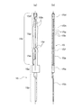
まず構成を説明すると、図中符号11は、「電気部品用ソケット」としてのICソケットで、このICソケット11は、「電気部品」であるICパッケージ12の性能試験を行うために、このICパッケージ12の「端子」としての半田ボール12bと、測定器(テスター)のプリント配線板(図示省略)との電気的接続を図るものである。
First, the configuration will be described.
このICパッケージ12は、図6に示すように、いわゆるBGA(Ball Grid Array)タイプと称されるもので、方形状のパッケージ本体12aの下面に多数の略球状の半田ボール12bが突出して縦列と横列とにマトリックス状に配列されている。
As shown in FIG. 6, the
一方、ICソケット11は、図2に示すように、大略すると、プリント配線板上に装着される合成樹脂製のソケット本体13を有し、このソケット本体13には、ICパッケージ12の各半田ボール12bに離接されるコンタクトピン15が配設されると共に、これらコンタクトピン15を変位させる移動部材17が配設され、更に、この移動部材17の上側に、収容部材19がそのソケット本体13に固定されて配設されている。さらにまた、その移動部材17を上下動させる操作部材21が配設されている。
On the other hand, as shown in FIG. 2, the
そのコンタクトピン15は、バネ性を有し、導電性に優れた板材がプレス加工により図6乃至図8に示すような形状に形成されている。
The
詳しくは、そのコンタクトピン15は、上下方向中間部に詳細は省略するが水平断面が略U字状の基部15aが形成されると共に、この基部15aの下側には、1本のソルダーテール部15bが形成され、上側には、一対の弾性片15cが形成されている。
Specifically, the
それら一対の弾性片15cは、下端部側の基部15aが略U字状に折曲されることにより、互いに対向するように形成されている。また、それら弾性片15cの上端部(先端部)には、ICパッケージ12の半田ボール12bの側部に離接する接触部15dが形成され、この両接触部15dで半田ボール12bが挟持されて電気的に接続されるようになっている。
The pair of
また、このコンタクトピン15の一対の弾性片15cは、下部15eが、ベース部14の挿通孔14aに挿通され、この下部15eの上側に側方に向けて突設された予圧突部15fが形成され、これら予圧突部15fがベース部14の挿通孔14aの内壁に当接されることにより、両接触部15dが閉じる方向に弾性変形されて予圧が付与されている。
The pair of
さらに、この一対の弾性片15cの、下部15eより上側には、接触部15dまでの間に、下部15e側とは互いに反対側に突出するように摺動部15gが形成され、これら摺動部15gがベース部14より上方に突出され、移動部材17の挿通孔17aに挿入されている。そして、この移動部材17が上下動されることにより、挿通孔17aの内壁が、摺動部15gを摺動して、弾性片15cが弾性変形されて、両接触部15dが開閉されるようになっている。
Further, a sliding
その移動部材17の挿通孔17aは、下方が広がるように形成される一方、弾性片15cの摺動部15gには、張出し部15hが形成され、この張出し部15hが押されることにより、図7に示すように、両接触部15dが開かれるように構成されている。
The
さらにまた、両接触部15dは、図6に示すように、最上昇位置の移動部材17より上方に突出し、摺動部15gの上端において、略直角に折曲げられ、互いに向き合い、これら両接触部15dにより、半田ボール12bが挟持されて、電気的に接続されるようになっている。
Furthermore, as shown in FIG. 6, the two
また、ベース部14の下側には、底板23が図2に示すように係止片23aにより、ベース部14に取り付けられ、この底板23の挿通孔23aに図4及び図6に示すように、コンタクトピン15のソルダーテール部15bが挿通され、この底板23とベース部14との間に、コンタクトピン15の基部15aが挟持され、その底板23により下方への移動が阻止されるように構成されている。
Further, on the lower side of the
さらに、この底板23の下側には、ロケートボード24が上下動自在に配設されている。そして、底板23から下方に突出したソルダーテール部15bは、図2及び図3に示すように、ロケートボード24を介して更に下方に突出され、図示省略のプリント配線板の各貫通孔に挿通されて半田付けされることにより接続されるようになっている。
Further, a locate
このようなコンタクトピン15は、図1に示すように、縦列と横列とにマトリックス状に配列されている。 Such contact pins 15 are arranged in a matrix in columns and rows as shown in FIG.
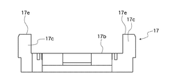
一方、移動部材17は、図9乃至図11に示すように、多数の挿通孔17aが形成されて略水平方向に沿う板状の移動部材本体17bと、この本体17bの端縁部から上方に突出された突出部17cとを有している。この突出部17cには、上端面に略水平方向に沿う被押圧面17eが形成されている。
On the other hand, as shown in FIGS. 9 to 11, the moving
また、この移動部材17は、コイルスプリング24により上方に付勢され、この移動部材17にベース部14から突設された係止部14bが図2に示すように係止されることにより、移動部材17の上昇が規制されるように構成されている。
The moving
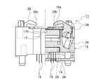
さらに、この移動部材17の上側で、突出部17cの内側には、枠形状の収容部材19が配設されている。この収容部材19は、パッケージ本体12aの周縁部を支持する支持片19aが形成され、この支持片19aの周縁部にガイド部19bが上方に向けて突設され、このガイド部19bにより、ICパッケージ12が収容時に案内されるようになっている。さらに、この収容部材19には、図2に示すように、係止部19cが下方に向けて突設され、この係止部19cがベース部14側に係止されることにより、収容部材19が着脱自在に取り付けられるようになっている。この収容部材19には、後述するラッチ部材28が出入りする開口19dが形成されている。
Further, a frame-shaped
このラッチ部材28は、図12乃至図14に示すように、回動軸28aを有し、この回動軸28aにより、ソケット本体13に回動自在に配設されると共に、図5に示すように、移動部材17の押圧部17dにより押圧される被押圧部28bが側方に一対突設されている。また、このラッチ部材28は、図3に示すように、スプリング29により閉じる方向に付勢され、先端部に設けられた押さえ部28cにより、ICパッケージ12の周縁部の上面に当接して、これを押さえるようにしている。
As shown in FIGS. 12 to 14, the
そして、移動部材17を下降させることにより、この移動部材17の押圧部17dにてラッチ部材28の被押圧部28bが押圧されて、図3中、実線に示す位置から二点鎖線に示す位置まで、ラッチ部材28が回動されて開かれ、このラッチ部材28の押さえ部28cがICパッケージ12の収容・取出し軌跡から退避されるように構成されている。
Then, by lowering the moving
また、操作部材21は、四角形の枠形状を呈し、収容部材19の周囲に配設され、ソケット本体13の周囲に上下動自在に配設され、この操作部材21の押圧面21aにより、移動部材17の突出部17cの上面に形成された被押圧面17eが押圧されて、コイルスプリング25の付勢力に抗して、移動部材17が下降されるように構成されている。
The
次いで、かかるICソケット11の使用方法について説明する。
Next, a method for using the
ICパッケージ12をICソケット11にセットするには、まず、操作部材21を下方に押し下げる。すると、この操作部材21により、移動部材17が下方に押されて、コイルスプリング25の付勢力に抗して下降される。
In order to set the
すなわち、図4に示す状態から、操作部材21が下降されると、この操作部材21の押圧面21aが、移動部材17の被押圧面17eに当接して押圧することにより、移動部材17が図5に示すように下降されることとなる。
That is, when the operating
この移動部材17の下降により、コンタクトピン15の両接触部15dが開かれると共に、ラッチ部材28も開かれることとなる。
As the moving
すなわち、移動部材17が下降すると、押圧部17dにより、ラッチ部材28の被押圧部28bが押されて、スプリング29の付勢力に抗して、ラッチ部材28が図2中二点鎖線に示す位置まで回動される。これにより、ラッチ部材28の押さえ部28cが、ICパッケージ12の収容・取出し軌跡から退避される。
That is, when the moving
また、コンタクトピン15は、図6に示す状態から図7に示す状態まで移動部材17が下降されると、この移動部材17の挿通孔17aの周壁に、弾性片15cの張出し部15hが押圧されることにより、両接触部15dが開かれる。
Further, when the moving
この状態で、ICパッケージ12がガイド部19bにガイド部されて、支持片19a上の所定位置に収容され、ICパッケージ12の各半田ボール12bが、各コンタクトピン15の開かれた一対の接触部15dの間に、非接触状態で挿入される(図7参照)。
In this state, the
その後、操作部材21の下方への押圧力を解除すると、この移動部材17がコイルスプリング25等の付勢力で上昇されることにより、ラッチ部材28がスプリング29の付勢力により閉じる方向に回動される。これにより、移動部材17にてICパッケージ12が押さえられ、浮き上がりが防止される。
Thereafter, when the downward pressing force of the
また、移動部材17が上昇されると、コンタクトピン15の摺動部15gへの押圧力が解除され、図7に示す状態から、一対の接触部15dが互いに閉じる(狭まる)方向に移動し、両接触部15dにて半田ボール12bが挟持される。
Further, when the moving
これにより、ICパッケージ12の各半田ボール12bとプリント配線板とがコンタクトピン15を介して電気的に接続されることとなる。
Thus, each
一方、ICパッケージ12を装着状態から取り外すには、同様に操作部材21を介して移動部材17を下降させることにより、ラッチ部材28が収容・取出し範囲から退避されると共に、コンタクトピン15の一対の接触部15dが半田ボール12bから離間されることから、半田ボール12bが一対の接触部15dにて挟まれた状態から引き抜く場合よりも弱い力で簡単にICパッケージ12を外すことができる。
On the other hand, in order to remove the
このようなものにあっては、移動部材17に、移動部材本体17bから上方に突出する突出部17cを形成し、この突出部17cの上面の被押圧面17eが操作部材21により直接押圧されるようにしているため、従来のようなリンク部材が必要なく、部品点数を削減できる。
In such a case, the moving
また、移動部材本体17bから上方に突出する突出部17cを形成することにより、操作部材21に移動部材17を押圧する突片を形成する必要がなく、構造を簡単にでき、強度及び耐久性を確保できる。ちなみに、操作部材21に下方に突出する突片を形成しようとすると、ソケット本体13内に入り込むような形状に形成しなければならないため、操作部材21の構造が複雑となると共に、突片の形状が細く、比較的弱い形状になってしまう。
Further, by forming the protruding
さらに、移動部材17の被押圧面17eは、水平面であり、押圧方向(上下方向)と直交する方向の面であるため、傾斜面と異なり、操作部材21の押圧面21aと、移動部材17の被押圧面17eとの間で、擦れるようなことが無く、耐久性を確保できる。
Furthermore, since the pressed
さらにまた、突出部17cの内側に、収容部材19を配設することにより、操作部材21にてその突出部17cを押圧する際に、収容部材19が邪魔にならない。また、上下動する移動部材17の上方で、ICパッケージ12を収容する必要があるため、収容部材19を突出部17cの内側に配置することにより、その収容部材19にICパッケージ12を良好に収容できる。
Furthermore, by disposing the accommodating
しかも、その収容部材19は、係止部19cによりソケット本体13に着脱自在に設けられているため、この収容部材19を外すことにより、移動部材17も簡単に外すことができる。
Moreover, since the
また、この収容部材19には、ガイド部19bを形成することにより、ICパッケージ12を所定の位置に良好に案内することができる。
[発明の実施の形態2]
Further, the
[Embodiment 2 of the Invention]
図15乃至図19には、この発明の実施の形態2を示す。 15 to 19 show a second embodiment of the present invention.
この実施の形態2は、実施の形態1と比較すると、操作部材21が設けられていないと共に、収容部材19は支持片19aのみで、ガイド部19bが設けられていない点で相違している。
The second embodiment is different from the first embodiment in that the operating
このようなものにあっては、図示していないが、パッケージ挿抜装置側のヘッドで、移動部材17の突出部17cの上面に形成された被押圧面17e(水平面)が直接押圧されるようになっている。
In such a case, although not shown, the pressed
従って、操作部材21が必要なく、部品点数を削減できると共に、移動部材本体17bから上方に突出する突出部17cを形成することにより、パッケージ挿抜装置側のヘッドに、移動部材17を押圧する突片を形成する必要がなく、構造を簡単にでき、強度及び耐久性を確保できる。ちなみに、パッケージ挿抜装置側のヘッドに、下方に突出する突片を、ソケット本体13内に入り込むような形状に形成しようとすると、操作部材21に形成する場合より、一層大変である。
Therefore, the
さらに、移動部材17の被押圧面17eは、水平面であり、押圧方向(上下方向)と直交する方向の面であるため、傾斜面と異なり、ヘッド側の押圧面と、移動部材17の被押圧面17eとの間で、擦れるようなことが無く、耐久性を確保できる。
Furthermore, since the pressed
他の構成及び作用は実施の形態1と同様であるので説明を省略する。 Since other configurations and operations are the same as those of the first embodiment, description thereof is omitted.
なお、上記実施の形態では、「電気部品用ソケット」としてICソケット11に、この発明を適用したが、これに限らず、他の装置にも適用できることは勿論である。また、BGAタイプのICパッケージ12用のICソケット11に、この発明を適用したが、これに限らず、PGA(Pin Grid Array)タイプのICパッケージ用のICソケットに、この発明を適用することもできる。さらに、この発明の移動部材の突出部は、移動部材本体から上方に突出していれば、上記実施の形態の突出部17cの形状や位置等に限定されるものでない。
In the above-described embodiment, the present invention is applied to the
11 ICソケット(電気部品用ソケット)
12 ICパッケージ(電気部品)
12a パッケージ本体
12b 半田ボール(端子)
13 ソケット本体
14 ベース部
14a 挿通孔
15 コンタクトピン
15a 基部
15c 弾性片
15d 接触部
15f 突部
17 移動部材
17a 挿通孔
17b 移動部材本体
17c 突出部
17d 押圧部
17e 被押圧面
19 収容部材
19a 支持片
19b ガイド部
21 操作部材
21a 押圧面
28 ラッチ部材
28a 回動軸
28b 被押圧部
28c 押さえ部
11 IC socket (socket for electrical parts)
12 IC package (electrical parts)
12a Package body
12b Solder ball (terminal)
13 Socket body
14 Base part
14a Insertion hole
15 Contact pin
15a base
15c elastic piece
15d contact area
15f protrusion
17 Moving member
17a Insertion hole
17b Moving member body
17c Protrusion
17d Pressing part
17e Pressed surface
19 Housing member
19a Support piece
19b Guide section
21 Operation parts
21a Press surface
28 Latch member
28a Rotation axis
28b Pressed part
28c Holding part
Claims (6)
前記移動部材は、前記複数のコンタクトピンが挿通される挿通孔が形成されて略水平方向に沿う移動部材本体と、該移動部材本体から上方に突設されて上端面に被押圧面が形成された突出部とを有し、該被押圧面が押圧されることにより、前記移動部材が下降されるように構成されたことを特徴とする電気部品用ソケット。 A plurality of contact pins having elastic pieces that can be separated from and connected to the terminals of the electrical component are disposed on the base portion of the socket body that accommodates the electrical component, and a moving member is movable up and down on the upper side of the base portion. The elastic piece of each contact pin is inserted into the moving member, and the elastic piece is opened and closed by moving the moving member up and down, so that both contact portions of the elastic piece are connected to the electrical component terminal. In the socket for electrical parts that is separated from
The moving member is formed with an insertion hole through which the plurality of contact pins are inserted, and a moving member main body extending in a substantially horizontal direction. The moving member protrudes upward from the moving member main body, and a pressed surface is formed on the upper end surface. A socket for an electrical component, wherein the moving member is lowered when the pressed surface is pressed.
Priority Applications (2)
| Application Number | Priority Date | Filing Date | Title |
|---|---|---|---|
| JP2004315344A JP4467404B2 (en) | 2004-10-29 | 2004-10-29 | Socket for electrical parts |
| US11/260,292 US7134892B2 (en) | 2004-10-29 | 2005-10-28 | Socket for electrical parts |
Applications Claiming Priority (1)
| Application Number | Priority Date | Filing Date | Title |
|---|---|---|---|
| JP2004315344A JP4467404B2 (en) | 2004-10-29 | 2004-10-29 | Socket for electrical parts |
Publications (2)
| Publication Number | Publication Date |
|---|---|
| JP2006127937A true JP2006127937A (en) | 2006-05-18 |
| JP4467404B2 JP4467404B2 (en) | 2010-05-26 |
Family
ID=36262627
Family Applications (1)
| Application Number | Title | Priority Date | Filing Date |
|---|---|---|---|
| JP2004315344A Expired - Fee Related JP4467404B2 (en) | 2004-10-29 | 2004-10-29 | Socket for electrical parts |
Country Status (2)
| Country | Link |
|---|---|
| US (1) | US7134892B2 (en) |
| JP (1) | JP4467404B2 (en) |
Cited By (2)
| Publication number | Priority date | Publication date | Assignee | Title |
|---|---|---|---|---|
| WO2009084085A1 (en) * | 2007-12-27 | 2009-07-09 | Yamaichi Electronics Co., Ltd. | Semiconductro device socket |
| WO2013042919A1 (en) * | 2011-09-23 | 2013-03-28 | 하이콘 주식회사 | Socket device for an ic test |
Families Citing this family (5)
| Publication number | Priority date | Publication date | Assignee | Title |
|---|---|---|---|---|
| JP5836113B2 (en) * | 2011-12-28 | 2015-12-24 | 株式会社エンプラス | Socket for electrical parts |
| TWM444623U (en) * | 2012-06-25 | 2013-01-01 | Hon Hai Prec Ind Co Ltd | Electrical connector |
| KR101944693B1 (en) * | 2018-12-04 | 2019-02-01 | 황동원 | BGA Socket device for testing an BGA IC |
| JP2022079959A (en) * | 2020-11-17 | 2022-05-27 | 山一電機株式会社 | Inspection socket |
| US11569601B2 (en) * | 2021-03-11 | 2023-01-31 | Enplas Corporation | Socket and inspection socket |
Family Cites Families (2)
| Publication number | Priority date | Publication date | Assignee | Title |
|---|---|---|---|---|
| US4480888A (en) * | 1982-06-23 | 1984-11-06 | Amp Incorporated | Multi terminal low insertion force connector |
| JP3683476B2 (en) | 2000-06-19 | 2005-08-17 | 株式会社エンプラス | Socket for electrical parts and method for assembling the same |
-
2004
- 2004-10-29 JP JP2004315344A patent/JP4467404B2/en not_active Expired - Fee Related
-
2005
- 2005-10-28 US US11/260,292 patent/US7134892B2/en not_active Expired - Fee Related
Cited By (6)
| Publication number | Priority date | Publication date | Assignee | Title |
|---|---|---|---|---|
| WO2009084085A1 (en) * | 2007-12-27 | 2009-07-09 | Yamaichi Electronics Co., Ltd. | Semiconductro device socket |
| KR101169153B1 (en) * | 2007-12-27 | 2012-07-30 | 야마이치덴키 가부시키가이샤 | Semiconductor device socket |
| US8272882B2 (en) | 2007-12-27 | 2012-09-25 | Yamaichi Electronics Co., Ltd. | Semiconductor device socket |
| JP5083327B2 (en) * | 2007-12-27 | 2012-11-28 | 山一電機株式会社 | Socket for semiconductor device |
| WO2013042919A1 (en) * | 2011-09-23 | 2013-03-28 | 하이콘 주식회사 | Socket device for an ic test |
| US9435853B2 (en) | 2011-09-23 | 2016-09-06 | Hicon Co., Ltd. | Socket device for an IC test |
Also Published As
| Publication number | Publication date |
|---|---|
| US7134892B2 (en) | 2006-11-14 |
| US20060094280A1 (en) | 2006-05-04 |
| JP4467404B2 (en) | 2010-05-26 |
Similar Documents
| Publication | Publication Date | Title |
|---|---|---|
| JP4729346B2 (en) | Socket for electrical parts | |
| US7214084B2 (en) | Socket for electrical parts | |
| JP4886997B2 (en) | Socket for electrical parts | |
| JP2003217774A (en) | Contact pin and ic socket | |
| US6439910B2 (en) | Rotatable guide member for a socket for electrical parts | |
| US7722376B2 (en) | Socket for electronic devices | |
| JP2003178851A (en) | Socket for electric component | |
| JP2006012491A (en) | Ic socket | |
| US7134892B2 (en) | Socket for electrical parts | |
| JP4237485B2 (en) | Socket for electrical parts | |
| KR20030004126A (en) | Socket for Electronic Element | |
| KR20010113539A (en) | Socket for electrical parts and method of assembling the same | |
| JP5518391B2 (en) | Socket for electrical parts | |
| JP2006127935A (en) | Socket for electric component | |
| KR20010015435A (en) | Socket for electrical parts | |
| US7407401B2 (en) | Socket for electrical parts | |
| JPH08273777A (en) | Ic socket | |
| JP3877652B2 (en) | Contact pin and socket for electrical parts | |
| JP3942936B2 (en) | Socket for electrical parts | |
| US6768653B2 (en) | Mount structure | |
| JP3822068B2 (en) | Socket for electrical parts | |
| JP4786414B2 (en) | Socket for electrical parts | |
| JP2004047163A (en) | Socket for electrical component | |
| JP2005174670A (en) | Open-top type ic socket | |
| JP2006294456A (en) | Ic socket |
Legal Events
| Date | Code | Title | Description |
|---|---|---|---|
| A621 | Written request for application examination |
Free format text: JAPANESE INTERMEDIATE CODE: A621 Effective date: 20071004 |
|
| A977 | Report on retrieval |
Free format text: JAPANESE INTERMEDIATE CODE: A971007 Effective date: 20091106 |
|
| A131 | Notification of reasons for refusal |
Free format text: JAPANESE INTERMEDIATE CODE: A131 Effective date: 20091117 |
|
| A521 | Request for written amendment filed |
Free format text: JAPANESE INTERMEDIATE CODE: A523 Effective date: 20100115 |
|
| TRDD | Decision of grant or rejection written | ||
| A01 | Written decision to grant a patent or to grant a registration (utility model) |
Free format text: JAPANESE INTERMEDIATE CODE: A01 Effective date: 20100223 |
|
| A01 | Written decision to grant a patent or to grant a registration (utility model) |
Free format text: JAPANESE INTERMEDIATE CODE: A01 |
|
| A61 | First payment of annual fees (during grant procedure) |
Free format text: JAPANESE INTERMEDIATE CODE: A61 Effective date: 20100223 |
|
| R150 | Certificate of patent or registration of utility model |
Free format text: JAPANESE INTERMEDIATE CODE: R150 |
|
| FPAY | Renewal fee payment (event date is renewal date of database) |
Free format text: PAYMENT UNTIL: 20130305 Year of fee payment: 3 |
|
| FPAY | Renewal fee payment (event date is renewal date of database) |
Free format text: PAYMENT UNTIL: 20130305 Year of fee payment: 3 |
|
| FPAY | Renewal fee payment (event date is renewal date of database) |
Free format text: PAYMENT UNTIL: 20140305 Year of fee payment: 4 |
|
| R250 | Receipt of annual fees |
Free format text: JAPANESE INTERMEDIATE CODE: R250 |
|
| R250 | Receipt of annual fees |
Free format text: JAPANESE INTERMEDIATE CODE: R250 |
|
| R250 | Receipt of annual fees |
Free format text: JAPANESE INTERMEDIATE CODE: R250 |
|
| LAPS | Cancellation because of no payment of annual fees |