JP2006114650A - Photolithography apparatus, scanning photolithography apparatus, device manufacturing method, original plate cleaning method, and the original plate - Google Patents
Photolithography apparatus, scanning photolithography apparatus, device manufacturing method, original plate cleaning method, and the original plate Download PDFInfo
- Publication number
- JP2006114650A JP2006114650A JP2004299790A JP2004299790A JP2006114650A JP 2006114650 A JP2006114650 A JP 2006114650A JP 2004299790 A JP2004299790 A JP 2004299790A JP 2004299790 A JP2004299790 A JP 2004299790A JP 2006114650 A JP2006114650 A JP 2006114650A
- Authority
- JP
- Japan
- Prior art keywords
- original
- stage
- light
- scanning
- cleaning
- Prior art date
- Legal status (The legal status is an assumption and is not a legal conclusion. Google has not performed a legal analysis and makes no representation as to the accuracy of the status listed.)
- Withdrawn
Links
Images


Classifications
-
- G—PHYSICS
- G03—PHOTOGRAPHY; CINEMATOGRAPHY; ANALOGOUS TECHNIQUES USING WAVES OTHER THAN OPTICAL WAVES; ELECTROGRAPHY; HOLOGRAPHY
- G03F—PHOTOMECHANICAL PRODUCTION OF TEXTURED OR PATTERNED SURFACES, e.g. FOR PRINTING, FOR PROCESSING OF SEMICONDUCTOR DEVICES; MATERIALS THEREFOR; ORIGINALS THEREFOR; APPARATUS SPECIALLY ADAPTED THEREFOR
- G03F7/00—Photomechanical, e.g. photolithographic, production of textured or patterned surfaces, e.g. printing surfaces; Materials therefor, e.g. comprising photoresists; Apparatus specially adapted therefor
- G03F7/70—Microphotolithographic exposure; Apparatus therefor
- G03F7/708—Construction of apparatus, e.g. environment aspects, hygiene aspects or materials
- G03F7/70908—Hygiene, e.g. preventing apparatus pollution, mitigating effect of pollution or removing pollutants from apparatus
- G03F7/70925—Cleaning, i.e. actively freeing apparatus from pollutants, e.g. using plasma cleaning
Landscapes
- Epidemiology (AREA)
- Engineering & Computer Science (AREA)
- Health & Medical Sciences (AREA)
- Physics & Mathematics (AREA)
- Public Health (AREA)
- Plasma & Fusion (AREA)
- Life Sciences & Earth Sciences (AREA)
- Atmospheric Sciences (AREA)
- Environmental & Geological Engineering (AREA)
- General Physics & Mathematics (AREA)
- Exposure And Positioning Against Photoresist Photosensitive Materials (AREA)
- Exposure Of Semiconductors, Excluding Electron Or Ion Beam Exposure (AREA)
- Preparing Plates And Mask In Photomechanical Process (AREA)
Abstract
Description
本発明は、原版上のパターンを基板に転写する露光技術に関する。また、特に、当該原版をクリーニングするための技術に関するものである。 The present invention relates to an exposure technique for transferring a pattern on an original to a substrate. In particular, the present invention relates to a technique for cleaning the original plate.
現在、DRAM、MPU、等の半導体デバイス製造に関して、デザインルールで100nm以下の線幅を有するデバイスの実現に向けて精力的に研究開発がなされている。この世代に用いられる露光装置として、極端紫外域光(EUV)を用いた露光装置が有力視されている。
一般に半導体露光装置は、回路パターンが描画されているレチクル(マスクともいう)に照明光を照射し、その回路パターン像を、投影光学系を用いて、例えば1/4に縮小して、感光体(レジスト)が塗布されているウエハーに投影露光するという構成となっている。従って、実際の露光では、レチクルの回路パターン面にパーティクルが付着すると、各ショットの全く同じ位置にパーティクル像が転写されることになる。このため半導体デバイス製造の歩留まりや、半導体デバイス自体の信頼性が大幅に低下するという致命的な問題があった。
Currently, with respect to the manufacture of semiconductor devices such as DRAMs, MPUs, etc., research and development has been vigorously carried out toward the realization of devices having a line width of 100 nm or less by design rules. As an exposure apparatus used in this generation, an exposure apparatus using extreme ultraviolet light (EUV) is considered promising.
In general, a semiconductor exposure apparatus irradiates a reticle (also referred to as a mask) on which a circuit pattern is drawn with illumination light, and reduces the circuit pattern image to, for example, 1/4 using a projection optical system. The wafer is coated with (resist) by projection exposure. Therefore, in actual exposure, when particles adhere to the circuit pattern surface of the reticle, a particle image is transferred to the exact same position in each shot. For this reason, there have been fatal problems that the yield of semiconductor device manufacturing and the reliability of the semiconductor device itself are greatly reduced.
この問題に対し、従来のg線、i線、KrFレーザー、ArFレーザー、等を光源に持つ露光装置では、レチクルにペリクルという透明保護膜を、回路パターン面から数mm間隔を空けて配置することで、回路パターンをパーティクル付着から保護していた。このペリクルに付着したパーティクルは回路パターン面である物体平面からかデフォーカスしているため、通常所定の大きさ以下のパーティクルであれば、ウエハー上には欠陥像として転写されない。 To solve this problem, in a conventional exposure apparatus having a g-line, i-line, KrF laser, ArF laser, etc. as a light source, a transparent protective film called a pellicle is disposed on the reticle at a distance of several mm from the circuit pattern surface. Thus, the circuit pattern was protected from particle adhesion. Since the particles adhering to the pellicle are defocused from the object plane which is the circuit pattern surface, if the particles are usually smaller than a predetermined size, they are not transferred as a defect image on the wafer.
しかし、本発明が適用されるEUV露光装置では、EUV光に対して透明なペリクルが存在しないのが現実である。要求される透過率を満たすためには、ペリクルの厚さを数10nm程度にせざるを得ず、このような厚さでは、レチクルを搬送する際、大気圧から真空環境下へ、逆に真空環境下から大気圧へというように雰囲気圧力変化に対する機械的側面、あるいは、EUV露光光が吸収され温度が上昇することによる熱的側面、の両方において、十分な強度で構成することが不可能であることがわかっている。 However, in an EUV exposure apparatus to which the present invention is applied, there is actually no pellicle that is transparent to EUV light. In order to satisfy the required transmittance, the thickness of the pellicle must be about several tens of nanometers. With such a thickness, when the reticle is transported, the atmospheric pressure changes from the atmospheric pressure to the vacuum environment. It is impossible to construct with sufficient strength both in the mechanical aspect against the atmospheric pressure change from the bottom to the atmospheric pressure, or in the thermal aspect due to the absorption of EUV exposure light and the temperature rising. I know that.
従って、EUV露光装置では、レチクルはペリクルレスとならざるを得ず、露光装置内でパーティクルが発生した場合、レチクル回路パターン面へのパーティクル付着が懸念される。 Therefore, in the EUV exposure apparatus, the reticle must be pellicle-less, and when particles are generated in the exposure apparatus, there is a concern that particles adhere to the reticle circuit pattern surface.
例えば、デザインルール35nmのデバイス製造を考えた場合、投影光学系の縮小倍率が4:1で、仮に0.1μmのパーティクルがレチクル回路パターンに付着するとウエハー上では、25nmとなるため、デバイス製造は不可能になる。実際には、管理すべき粒径はさらに小さくなり、数十nm以下の極めて微小なパーティクルとなる。 For example, when a device with a design rule of 35 nm is considered, the reduction ratio of the projection optical system is 4: 1, and if a 0.1 μm particle adheres to the reticle circuit pattern, it becomes 25 nm on the wafer. It becomes impossible. In practice, the particle size to be managed is even smaller, resulting in extremely fine particles of several tens of nm or less.
このように装置内で発生するナノメートルサイズのパーティクルは、その発生原因、その挙動に対し十分解明されているとは言えないが、想定される発生原因としては、レチクルステージ、ロボットハンド、ゲートバルブの動作等、摺動、摩擦により発生するパーティクル、光源側からわずかながら飛翔してくるデブリ、などが予想される。 The nanometer-sized particles generated in the device are not well understood for the cause and behavior of the particles, but the possible causes are the reticle stage, robot hand, and gate valve. It is expected that particles generated by sliding and friction, debris flying slightly from the light source side, etc.
また、EUV露光装置の露光は真空中で行うため、必然的にレチクルの搬入、搬出にはロードロックチャンバーを介して行うことになるが、ここでもパーティクルの付着が懸念される。その原因としては、ロードロック内が真空排気される際に、チャンバー内に存在しているパーティクルが気流の発生により、剥離し、レチクルパターン面に付着するとされている。 In addition, since the exposure of the EUV exposure apparatus is performed in a vacuum, the reticle is inevitably carried in and out through the load lock chamber. However, there is a concern about the adhesion of particles. The cause is that when the inside of the load lock is evacuated, the particles existing in the chamber are peeled off due to the generation of the air current, and adhere to the reticle pattern surface.
また、パーティクルの真空中で想定される挙動は、ガス分子がほとんど存在しないため、発生したパーティクルは流体抵抗を受けず、重力のみの力が作用する。このような場合、パーティクルが、チャンバー内壁と弾性衝突に近い衝突をすると、パーティクルはチャンバー内を跳ね回っているような挙動を示すという報告もある。あるいは、摩擦によって生じたパーティクルは電荷をもっていると予測されるため、0Vに接地された部材でも、パーティクルと部材間に電気映像効果とよばれる力が働き、付着すると考えられている。いずれにせよ、パーティクルの発生原因、及びその真空中での挙動に対し十分解明されているとは言えず、それに対する対策手段も非常に困難なものとなっている。 In addition, the behavior assumed in the vacuum of the particles is that there are almost no gas molecules, so the generated particles are not subjected to fluid resistance, and the force of only gravity acts. In such a case, there is a report that when a particle collides with the inner wall of the chamber close to an elastic collision, the particle behaves like bouncing around the chamber. Alternatively, since particles generated by friction are expected to have electric charges, even a member grounded at 0 V is considered to adhere to the particles and a force called an electro-image effect. In any case, it cannot be said that the cause of the generation of particles and the behavior thereof in a vacuum have been sufficiently elucidated, and countermeasures against them are extremely difficult.
このような露光チャンバー内でのレチクル回路パターン面へのパーティクル付着の問題に対し、二つのアプローチ方法が考えられている。すなわち、パーティクルが発生しレチクル近傍に飛散してきても付着を抑制する方法と、パーティクルが付着したらそれを除去する方法である。 Two approaches have been considered for the problem of particle adhesion to the reticle circuit pattern surface in the exposure chamber. That is, there are a method of suppressing adhesion even when particles are generated and scattered in the vicinity of the reticle, and a method of removing particles when they are adhered.
後者のアプローチ法に対しては、露光チャンバー内で、真空環境を維持した状態でパーティクルを効果的に除去する手段として、従来より、パルスレーザー照射除去法が提案されている。これは、nsオーダーのパルス光を照射することによって、付着パーティクルや基板の表面にnsオーダーの短時間に熱膨張が生じ、それにより発生する加速度が、パーティクルの付着力より大きくなると、パーティクルが基板より離脱し、除去されるというメカニズムで説明される。この技術を用いた例としては、特公平6−95510号公報(特許文献1)では、マスク表面を損傷せずに除去可能なパワー密度でレーザー照射するレーザー手段と、レーザー照射を行うことを可能にするためにマスクを露光時の位置からたたみ上げる手段とを設けている。また、特開2000−088999号公報(特許文献2)では、露光装置内に、X線光学素子(レチクル含む)にパルス状のレーザー光(KrFエキシマレーザー)を入射させる機構を設け、一定期間が経過した後に、真空チャンバー内に不活性ガスを導入しレチクルの表面にレーザー光を照射する、等の方法が提案されている。
しかしながら前述の背景技術では、次のような点で不十分な点があった。 However, the above-described background art is insufficient in the following points.
特公平6−95510では、マスクに付着したパーティクルをパルスレーザー光照射によりクリーニングする際、マスクは露光時の位置とは別の位置に移動して、クリーニングが行われる。従って、マスクがクリーニングされている間は、露光が行われることはなく、大きなスループットの低下を招くことになる。また、マスクが別の位置に移動する際、摺動、摩擦によりパーティクルが発生し、クリーニングした後もパーティクルが付着する懸念がある。 In Japanese Examined Patent Publication No. 6-95510, when cleaning particles adhering to the mask by irradiating with pulsed laser light, the mask is moved to a position different from the position at the time of exposure, and cleaning is performed. Therefore, exposure is not performed while the mask is being cleaned, resulting in a significant reduction in throughput. Further, when the mask moves to another position, particles are generated due to sliding and friction, and there is a concern that the particles adhere after cleaning.
また、特開2000−088999では、レチクルをパルスレーザーでクリーニングする際、不活性ガスをチャンバー内に導入するとしている。この理由は、パルスレーザー照射でレチクル表面からパーティクルが離脱した場合、ガスが導入されていると、パーティクルの運動を抑制する流体抗力が作用し、パーティクルがガスにトラップされるため、チャンバー内にガスを一定の流量供給し、回収することで、パーティクルをガスごと空間内から除去することを可能にするためである。しかし、EUV露光装置は、前述したが真空チャンバー内は高真空(10E−3〜−5Pa)環境であるため、チャンバー内に一旦パーティクル除去用のガスを導入すると、クリーニングが終了してから再び高真空環境に戻すためには、チャンバー容積や真空ポンプの排気速度にもよるが、最低数時間はかかると予測される。従って、この時間は、装置はまったく露光が不可能になり、装置の有効稼働率を著しく落とすことになる。 In Japanese Patent Laid-Open No. 2000-088999, an inert gas is introduced into the chamber when the reticle is cleaned with a pulse laser. The reason for this is that when particles are detached from the reticle surface by pulse laser irradiation, if a gas is introduced, fluid drag that suppresses the movement of the particles acts and traps the particles in the gas. This is because the particles can be removed from the space together with the gas by supplying and collecting a constant flow rate of the gas. However, as described above, since the EUV exposure apparatus is in a high vacuum environment (10E-3 to -5 Pa) in the vacuum chamber, once the gas for removing particles is introduced into the chamber, the cleaning is completed and then the high pressure is again applied. In order to return to the vacuum environment, although it depends on the chamber volume and the pumping speed of the vacuum pump, it is expected to take a minimum of several hours. Therefore, during this time, the apparatus cannot be exposed at all, and the effective operating rate of the apparatus is significantly reduced.
また、前述の背景技術に共通することとして、問題となる粒径のパーティクルがレチクルに付着しても、それが除去されるまで露光が行われるとすると、付着してから以降のショットはすべてNGとなることになり、デバイス製造の歩留まりを大きく低下させることになる。特に、真空チャンバー内でのパーティクルの発生原因や、その挙動に対しては、前述のように十分解明されているものではなく、マスクへのパーティクル付着はまったくランダムな、再現性のない現象であると予想されるため、上述の背景技術のようにパルスレーザークリーニング手段を設けているだけでは、実際の製造現場では、この技術を効果的に適用することは不可能である。このことに対応して、レチクルの微粒子の付着を露光動作中常にモニターする手段があれば、パーティクルが付着したことを検出して、すぐさまクリーニング動作に移ることも可能であるが、実際、高速でスキャン駆動するレチクル表面に付着した、例えば数10nmの粒子をリアルタイムで検出することは現状の技術ではまったく不可能である。 Further, in common with the above-described background art, even if a particle having a particle size in question adheres to the reticle, if exposure is performed until it is removed, all subsequent shots after the adhesion are NG. As a result, the device manufacturing yield is greatly reduced. In particular, the cause and behavior of particles in the vacuum chamber have not been fully elucidated as described above, and particle adhesion to the mask is a completely random and non-reproducible phenomenon. Therefore, it is impossible to effectively apply this technique at an actual manufacturing site only by providing the pulse laser cleaning means as in the background art described above. Corresponding to this, if there is a means to constantly monitor the adhesion of fine particles on the reticle during the exposure operation, it is possible to detect the adhesion of the particles and immediately start the cleaning operation. For example, it is impossible to detect particles of, for example, several tens of nanometers attached to the surface of the reticle to be scanned in real time with the current technology.
以上のように、上述の背景技術はレチクル(マスク)に付着したパーティクルを除去することはできても、クリーニングの際は大きなスループットの低下、あるいは装置稼働率の低下をもたらし、また、レチクルにパーティクルが付着した際のデバイス製造の歩留まり低下を完全に防ぐことは不可能であった。 As described above, although the above-mentioned background art can remove particles adhering to the reticle (mask), it causes a large decrease in throughput or a reduction in apparatus operation rate during cleaning, and particles on the reticle It was impossible to completely prevent a decrease in the yield of device manufacturing when adhering.
本発明は、上述の背景技術を考慮してなされたもので、スループットおよびクリーニング性能の観点で有利な、原版のクリーニング技術を提供することを例示的目的とする。 The present invention has been made in view of the above-described background art, and an object of the present invention is to provide an original plate cleaning technique that is advantageous in terms of throughput and cleaning performance.
第1の発明は、原版を保持する原版ステージと、露光用光源からの光により前記原版ステージに保持された原版を照明するための照明光学系と、前記原版上のパターンを基板に投影するための投影光学系とを有する露光装置において、クリーニング用の光を前記原版ステージに保持された原版に照射する照射手段を有することを特徴とする露光装置である。 According to a first aspect of the present invention, there is provided an original stage for holding an original, an illumination optical system for illuminating the original held on the original stage by light from an exposure light source, and a pattern on the original to be projected onto a substrate. In the exposure apparatus having the projection optical system, the exposure apparatus includes an irradiation unit that irradiates the original held on the original stage with cleaning light.
第2の発明は、原版を保持し走査方向に移動する原版ステージと、露光用光源からの光により前記原版ステージに保持された原版を照明するための照明光学系と、基板を保持し走査方向に移動する基板ステージと、前記原版上のパターンを前記基板に投影するための投影光学系とを有する走査露光装置において、クリーニング用の光を前記原版ステージに保持された原版に照射する照射手段を有することを特徴とする走査露光装置である。 According to a second aspect of the present invention, there is provided an original stage for holding an original and moving in the scanning direction, an illumination optical system for illuminating the original held on the original stage by light from an exposure light source, and a scanning direction for holding a substrate. In a scanning exposure apparatus having a substrate stage that moves to a substrate and a projection optical system for projecting a pattern on the original onto the substrate, an irradiating means for irradiating the original held on the original stage with cleaning light It is a scanning exposure apparatus characterized by having.
第3の発明は、上記第1の発明の露光装置および上記第2の発明の走査露光装置のいずれかを用いて原版上のパターンを基板に投影する投影工程と、前記投影工程において前記パターンが投影された基板を現像する現像工程とを有することを特徴とするデバイス製造方法である。 According to a third aspect of the present invention, there is provided a projection step of projecting a pattern on an original onto a substrate using any one of the exposure apparatus of the first aspect of the invention and the scanning exposure apparatus of the second aspect of the invention; And a developing process for developing the projected substrate.
第4の発明は、原版を保持する原版ステージと、露光用光源からの光により前記原版ステージに保持された原版を照明するための照明光学系と、前記原版上のパターンを基板に投影するための投影光学系とを有する露光装置における原版のクリーニング方法であって、クリーニング用の光を前記原版ステージに保持された原版に照射する照射工程を有することを特徴とする原版のクリーニング方法である。 According to a fourth aspect of the present invention, there is provided an original stage holding the original, an illumination optical system for illuminating the original held on the original stage by light from an exposure light source, and projecting a pattern on the original onto a substrate. An original plate cleaning method in an exposure apparatus having a projection optical system comprising: an irradiation step of irradiating the original plate held on the original stage with a cleaning light.
第5の発明は、原版を保持し走査方向に移動する原版ステージと、露光用光源からの光により前記原版ステージに保持された原版を照明するための照明光学系と、基板を保持し走査方向に移動する基板ステージと、前記原版上のパターンを前記基板に投影するための投影光学系とを有する走査露光装置における原版のクリーニング方法であって、クリーニング用の光を前記原版ステージに保持された原版に照射する照射工程を有することを特徴とする原版のクリーニング方法である。 According to a fifth aspect of the invention, there is provided an original stage that holds the original and moves in the scanning direction, an illumination optical system for illuminating the original held on the original stage by light from an exposure light source, and a scanning direction that holds the substrate. And a projection optical system for projecting a pattern on the original plate onto the substrate. A cleaning method for the original plate, wherein cleaning light is held on the original stage. An original plate cleaning method comprising an irradiation step of irradiating an original plate.
第6の発明は、露光光を反射する多層膜と、キャップ層とを有し、前記露光光によりパターンを基板に転写するための原版であって、前記多層膜と前記キャップ層との間に、前記露光光に関してよりも前記原版をクリーニングするための光に関して吸収係数が大きい層を有することを特徴とする原版である。 A sixth invention includes a multilayer film that reflects exposure light and a cap layer, and is an original plate for transferring a pattern to a substrate by the exposure light, and is provided between the multilayer film and the cap layer. A master having a layer having a larger absorption coefficient with respect to light for cleaning the master than with respect to the exposure light.
他の発明の特徴ならびにそれに対応した目的および優位性は、添付図面を参照してなされた後述の説明で明らかにされている。尚、当該図面において、同一又は類似の符号は複数の図面を通して同一又は類似の構成要素を表す。 Other features of the invention and corresponding objects and advantages will become apparent from the following description made with reference to the accompanying drawings. In the drawings, the same or similar reference numerals represent the same or similar components throughout the drawings.
本発明によれば、スループットおよびクリーニング性能の観点で有利な、原版のクリーニング技術を提供することができる。 According to the present invention, it is possible to provide an original plate cleaning technique that is advantageous in terms of throughput and cleaning performance.
以下に、本発明に係る実施の形態について添付図面を参照して詳細に説明する。 Embodiments according to the present invention will be described below in detail with reference to the accompanying drawings.
実施例1の詳細について説明する前に、本発明が適用されるEUV露光装置を例に挙げ、その構成を図3を用いて簡単に説明する。 Before describing the details of the first embodiment, an EUV exposure apparatus to which the present invention is applied will be described as an example, and its configuration will be briefly described with reference to FIG.
同図で、1はウエハー、2は電子回路パターンが形成されている反射型レチクルで、3はその反射型レチクルを保持し、スキャン方向に粗微動させるためのレチクルステージである。5はレチクルからのEUV反射光29をウエハー1に投影露光するための光学系である。6はウエハーを保持して6軸方向に粗動、微動可能なウエハーステージであり、そのxy位置は不図示のレーザー干渉計によって常にモニターされている。通常、レチクルステージ3とウエハーステージ6のスキャン動作は、投影光学系の縮小倍率を1/βとし、レチクルステージの走査速度をVr、ウエハーステージの走査速度をVwとすると、両者の走査速度の間には、Vr/Vw=βの関係が成立するように同期制御される。露光は真空環境下で行われるため、前述したそれぞれのユニットは露光装置チャンバー4の中に入っており、7は露光チャンバー内を真空排気するための真空ポンプである。
In the figure,
15はウエハーロードロックチャンバーであり、8はウエハーロードロックチャンバー15とウエハーステージ6との間でウエハーを搬入、搬出する搬送ハンドである。9はウエハーロードロック内を真空排気するための真空ポンプで、真空状態を大気圧に戻す際のドライN2,ドライエア、等のベント用ガス供給源とともに用いられる。11は装置チャンバーとウエハーロードロックチャンバーとの間を仕切る装置側ゲートバルブ、12はロードロックチャンバーと後述するウエハー交換室との間を仕切る交換室側ゲートバルブである。14はウエハーを大気圧下で一時保管するウエハー交換室であり、13はロードロックとの間でウエハーを搬入、搬出する搬送ハンドである。
Reference numeral 15 denotes a wafer load lock chamber, and reference numeral 8 denotes a transfer hand for loading and unloading the wafer between the wafer load lock chamber 15 and the
23はレチクルロードロックチャンバーであり、22はレチクルロードロックチャンバー23とレチクルステージ3との間でウエハーを搬入、搬出する搬送ハンドである。10はレチクルロードロック内を真空排気するための真空ポンプで、真空状態を大気圧に戻す際のドライN2,ドライエア、等のベント用ガス供給源とともに用いられる。16は装置チャンバーとレチクルロードロックチャンバーとの間を仕切る装置側ゲートバルブ、17はロードロックチャンバーと後述するレチクル交換室との間を仕切る交換室側ゲートバルブである。19はレチクルを大気圧下で一時保管するレチクル交換室であり、13はロードロックとの間でウエハーを搬入、搬出する搬送ハンドである。
20は本発明で用いるパルスレーザー光源であり、光源から射出したパルス光はチャンバーのレーザー光導入窓21を介して、真空チャンバー内に導入され、不図示の光学系によりビームが整形され、角度可変な反射ミラー22によりレチクル上に跳ね上げられ、レチクル回路パターンに照射される。以上が本発明を適用したEUV露光装置の説明である。
次に本発明の第1の実施例について図1を用いて説明する。図1は本発明の構成の正面図である。2はレチクルであり、回路パターン面が下面に形成されている。照明光学系から出射してきたEUV光29は下方からレチクルに入射し、回路パターン面で反射し、その反射光が投影光学系に入射する構成となっている。24はレチクルを吸着保持するためのチャックホルダーであり、これはレチクルのスキャンステージ25に微動機構を介して設けられている。露光中、レチクルステージは、同図のY軸方向に加速、等速、減速を繰り返し、スキャン運動をする。
Next, a first embodiment of the present invention will be described with reference to FIG. FIG. 1 is a front view of the configuration of the present invention. A
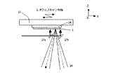
20はパーティクル除去用のパルスレーザー光源であり、主にKrFレーザー(波長248nm)、YAGレーザー(波長1064nm、他)などが用いられる。70は射出ビームを平行光にするための整形光学系、21は露光チャンバー隔壁に設けられたパルスレーザー導入窓で石英ガラスなど、入射波長に対して吸収の少ない光学材料で構成されている。26は、入射パルスビームを、パーティクルを除去するために適切なビーム形状に集光するための光学系であり、集光されたビームは22のミラーで跳ね上げられ、レチクルパターン面に照射される。本実施例では照射されたパルスレーザーはスキャン方向と直行する方向(同図でX方向)に長いシート状のビームに整形されている。
図2に、レチクル位置と、パーティクル除去用パルスレーザー照射位置と、EUV露光光照射位置との相対位置関係を示す。30はレチクル上のパーティクル除去範囲であり、31はレチクルスキャン方向(Y方向)と直交する方向(X方向)に、光学系によりシート状に整形されたパルスレーザー光断面で、パーティクル除去範囲30を十分に覆う長さを有している。32はEUV露光光で、図ではEUV露光光は長方形の形状としているが、これは照明光学系の特性により、円弧状の場合も考えられる。このように、除去用パルスレーザーをスキャン方向とは直交する方向(X方向)に長いシート状のビームに形成し、EUV露光光照射位置の近傍で、それと平行な位置で除去ビームを照射することで、レチクルステージが露光時に往復運動することを利用し、パーティクル除去範囲全域に常にパルスレーザー照射が可能になる。
FIG. 2 shows a relative positional relationship among the reticle position, the particle removal pulse laser irradiation position, and the EUV exposure light irradiation position. 30 is a particle removal range on the reticle, 31 is a pulse laser beam section shaped into a sheet shape by an optical system in a direction (X direction) orthogonal to the reticle scan direction (Y direction). It has sufficient length to cover.
次に、パルスレーザーを照射して、パーティクルを除去する際、有効な除去率を得るために、ステージスキャン速度Vs、パルスレーザーのパルス繰り返し周波数F、照射パルス数N、シートビーム幅Wについて説明する。 Next, the stage scan speed Vs, the pulse repetition frequency F of the pulse laser, the number of irradiation pulses N, and the sheet beam width W will be described in order to obtain an effective removal rate when particles are removed by irradiation with a pulse laser. .
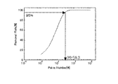
パルスレーザー照射法において、本発明者が行った実験では、基板上に付着したパーティクルは、パルスをより多く当てることでその除去率が向上した。図4はこれの概略を示したもので、例えば粒径0.1μmのパーティクルに対し、ある特定のレーザー照射条件で、1パルスでは10%程度の除去率しか望めないものの、パルス数を多くすると除去率は次第に向上し、この例では、80パルス程度照射するとほぼ100%の除去率となる。一般的に、粒子が基板に付着した際の付着力は、主に分子間力(Van der Waals力)、液架橋力、静電気力とされているが、通常の環境下では、分子間力(Van der Waals力)が主なものである。実験結果は、パルスを多く当てることで、パーティクルが基板に付着している際の付着力が徐々に弱くなって除去されると考えられる。また、パルスレーザーを照射した際の表面ダメージは、パルスエネルギーの積分値ではなく、1パルスあたりのエネルギー密度であるとの報告もあり、この事実は発明者が行った実験でも同様な結果が得られている。 In an experiment conducted by the present inventor in the pulse laser irradiation method, the removal rate of particles adhering to the substrate was improved by applying more pulses. FIG. 4 shows an outline of this. For example, for a particle having a particle diameter of 0.1 μm, a removal rate of about 10% can be expected with one pulse under a specific laser irradiation condition, but when the number of pulses is increased. The removal rate is gradually improved. In this example, when about 80 pulses are irradiated, the removal rate is almost 100%. In general, the adhesion force when a particle adheres to a substrate is mainly an intermolecular force (Van der Waals force), a liquid crosslinking force, or an electrostatic force. However, in a normal environment, the intermolecular force ( The Van der Waals force) is the main one. As a result of the experiment, it is considered that by applying many pulses, the adhesion force when the particles are adhered to the substrate gradually weakens and is removed. In addition, it has been reported that the surface damage when irradiated with a pulse laser is not the integrated value of the pulse energy but the energy density per pulse, and this fact is also obtained in experiments conducted by the inventors. It has been.
以上の実験事実は、パルスレーザーをレチクル多層膜に照射した際の最大の課題である表面ダメージ問題において、ダメージを与えない低エネルギー密度の照射では、1パルスあたりの除去率は低いものの、パルス数を多くすると十分な除去率を達成できる事実を示している。従って、実際の装置に適用した場合、必要とされる照射パルス数Nは、付着しているパーティクル材質、パルスエネルギー密度にも依存するため、あらかじめ実験で求めておく必要がある。例えば、この例では95%以上の除去率が必要な場合は、30パルス以上照射する必要があるということになる。 The above experimental fact is that, in the surface damage problem, which is the biggest problem when irradiating a reticle multilayer film with a pulse laser, the irradiation rate at low energy density that does not cause damage is low, but the number of pulses is low. This indicates the fact that a sufficient removal rate can be achieved by increasing. Therefore, when applied to an actual apparatus, the required number of irradiation pulses N depends on the adhering particle material and pulse energy density, and therefore needs to be obtained in advance by experiments. For example, in this example, when a removal rate of 95% or more is required, it is necessary to irradiate 30 pulses or more.
図2で、レチクルの等速時の運動速度をVs[m/s]、パルスレーザーのシートビーム厚をW[m]、パルスレーザーの繰り返し周波数をF[Hz]、除去に必要なパルス数をN[#]とする。レチクルがビーム厚Wを移動するのに要する時間△Tsは、
△Ts=W/Vs (1)
である。この時間内に移動する照射エリアに対し、最低N回のパルス照射が必要だとすると、このときのパルス時間間隔は、
△Tp=△Ts/N=W/(Vs*N) (2)
となる。一方、パルスレーザー光源のパルス時間間隔△τは、
△τ=1/F (3)
となる。△Tpは、△τよりも大きくなければシステムとして成立しないので、
W/(Vs*N)>1/F (4)
∴(Vs*N)/W<F (5)
In FIG. 2, the movement speed of the reticle at constant speed is Vs [m / s], the sheet beam thickness of the pulse laser is W [m], the repetition frequency of the pulse laser is F [Hz], and the number of pulses necessary for removal is shown. Let N [#]. The time ΔTs required for the reticle to move the beam thickness W is
ΔTs = W / Vs (1)
It is. Assuming that at least N pulse irradiations are required for the irradiation area moving within this time, the pulse time interval at this time is
ΔTp = ΔTs / N = W / (Vs * N) (2)
It becomes. On the other hand, the pulse time interval Δτ of the pulse laser light source is
Δτ = 1 / F (3)
It becomes. Since ΔTp is not established as a system unless it is larger than Δτ,
W / (Vs * N)> 1 / F (4)
∴ (Vs * N) / W <F (5)
すなわち所望の除去率(Nパルス照射に相当)を得るためには、レチクルの等速時の運動速度Vs[m/s]、パルスレーザーのシートビーム厚W[m]、パルスレーザーの繰り返し周波数F[Hz]に関し、(5)式のような簡単な関係式が成立するということである。例えば、Vs=100[mm/s],F=300[Hz],N=30[#]とすると(5)式より、シートビーム厚Wは10[mm]以上必要となる。 That is, in order to obtain a desired removal rate (corresponding to N pulse irradiation), the motion speed Vs [m / s] of the reticle at the constant speed, the sheet beam thickness W [m] of the pulse laser, and the repetition frequency F of the pulse laser With regard to [Hz], a simple relational expression such as the expression (5) is established. For example, when Vs = 100 [mm / s], F = 300 [Hz], and N = 30 [#], the sheet beam thickness W needs to be 10 [mm] or more from the equation (5).
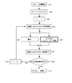
次に、レチクルにパルスレーザーを照射するタイミングについてフローチャートを使って説明する。図5はレチクルにパルスレーザーを照射するタイミングを露光と同時に行うことを特徴としている。先ず、所望のレイヤーを露光するために、既にレチクルは露光装置にロードされレチクルアライメントも完了しているとする。ウエハーがステージ上にロードされウエハー処理が開始される(101)。露光に先立ちウエハーがアライメントされ(102)、ショット番号を表す引数iが1にセットされる。第1ショットのスキャン動作が開始されると(104)、レチクルとウエハーは、例えば4:1の速度比で同期スキャンを行い、それぞれのステージの位置偏差が所定の目標値に入ると露光が行われ(105)、かつそれと並行してレチクルの露光光照射位置の近傍にパーティクル除去用のパルスレーザーが照射される(106)。これらが終了すると第1番目のショットの露光動作が終了する(107)。この時点では、第1ショットの露光が終了したのみなのでステップ108はNoとなり、ショット番号iをインクリメントし(109)、再び第2ショットの露光動作に移る(104)。以上の動作を繰り返し、1枚のウエハーに所望のショット数、Nショット露光すると1枚のウエハー処理が完了し、次のウエハー処理のステップに移る(110)。この例では、レチクルにパルスレーザーを照射するタイミングは、露光と同時並行して行われるため、スループットを低下させることなく、常にレチクルを清浄な状態に保つことが可能になる。 Next, the timing for irradiating the reticle with the pulse laser will be described with reference to a flowchart. FIG. 5 is characterized in that the timing of irradiating the reticle with the pulse laser is performed simultaneously with the exposure. First, in order to expose a desired layer, it is assumed that the reticle has already been loaded into the exposure apparatus and the reticle alignment has been completed. A wafer is loaded on the stage and wafer processing is started (101). Prior to exposure, the wafer is aligned (102), and an argument i representing a shot number is set to 1. When the scanning operation of the first shot is started (104), the reticle and wafer are scanned synchronously at a speed ratio of 4: 1, for example, and exposure is performed when the positional deviation of each stage reaches a predetermined target value. In parallel with this, a pulse laser for particle removal is irradiated in the vicinity of the exposure light irradiation position of the reticle (106). When these are finished, the exposure operation for the first shot is finished (107). At this point, since the exposure of the first shot is only completed, step 108 is No, the shot number i is incremented (109), and the exposure operation for the second shot is started again (104). The above operation is repeated, and when one wafer is exposed for a desired number of shots and N shots, one wafer processing is completed, and the process proceeds to the next wafer processing step (110). In this example, the timing of irradiating the reticle with the pulse laser is performed in parallel with the exposure, so that the reticle can always be kept clean without reducing the throughput.
図6はパルスレーザーを照射するタイミングを、ウエハー交換、アライメント時に行うことを特徴としている。先ず、所望のレイヤーを露光するために、既にレチクルは露光装置にロードされレチクルアライメントも完了しているとして、ロット処理が開始される(111)。ウエハー番号を表す引数jが1にセットされ(112)、ウエハーステージに1枚目のウエハーがロードされる(113)。1枚目のウエハー処理が開始され(114)、露光に先立ちウエハーはアライメント計測される(116)。一方、ステップ113、114、116と同時並行して、レチクルステージは、パルスレーザー照射のためにダミー動作が開始される(121)。次にレチクルに実際にパーティクル除去用のパルスレーザーが照射され(115)、照射が終了するとステージのダミー動作も終了する。この一連のパルスレーザー照射動作ステップ121、115、122は、前述のウエハー処理ステップ113,114,116を行っている間に完了すればよいので、レチクルステージのダミー動作と、レーザー照射の回数は1スキャンに制限されることはない。ステップ116と122が終了すると、1枚目ウエハーの各ショットの露光となり(117)、全ショットの露光が完了すると1枚目ウエハー処理が全て完了する(118)。この時点では、ウエハー1枚の露光動作が終了したのみなので、ステップ119の判断はNoとなり、ウエハー番号引数jをインクリメントして(120)、2枚目のウエハー処理に移行するために、ウエハーがステージ上にロードされる(113)。そして、2枚目の処理が開始されるが(114)、前述のようにステップ113,114,116と同時並行して、一連のパルスレーザー照射動作121,115,122が行われる。以上の動作を繰り返し、M枚全てのウエハーに対し一連の露光動作が完了すると(119)、次のロット処理へ移行する(121)。この例では、レチクルにパルスレーザーを照射するタイミングは、ウエハー交換とアライメント動作と同時並行して行われるため、スループットを低下させることなく、常にレチクルを清浄な状態に保つことが可能になる。
FIG. 6 is characterized in that the pulse laser irradiation is performed at the time of wafer exchange and alignment. First, in order to expose a desired layer, lot processing is started (111) assuming that the reticle has already been loaded into the exposure apparatus and reticle alignment has been completed. An argument j representing the wafer number is set to 1 (112), and the first wafer is loaded onto the wafer stage (113). The first wafer processing is started (114), and the wafer is subjected to alignment measurement prior to exposure (116). On the other hand, in parallel with steps 113, 114, and 116, the reticle stage starts a dummy operation for pulse laser irradiation (121). Next, the reticle is actually irradiated with a pulse laser for particle removal (115), and when the irradiation is completed, the dummy operation of the stage is also ended. Since this series of pulse laser irradiation operation steps 121, 115, and 122 may be completed while the above-described wafer processing steps 113, 114, and 116 are performed, the reticle stage dummy operation and the number of times of laser irradiation are one. You are not limited to scanning. When steps 116 and 122 are completed, the exposure of each shot of the first wafer is completed (117), and when the exposure of all shots is completed, the first wafer processing is completed (118). At this time, since the exposure operation for one wafer is only completed, the determination in
パルスレーザーを照射するタイミングとして、これ以外にも例えば、レチクルロードロックからレチクルが装置内に搬入された時点としても良いし、あるいは前述の例を組み合わせたタイミングで行っても良い。さらには、レチクルに付着するパーティクルが少ない場合は、これらの動作を間引いて行ってもかまわない。 In addition to this, the pulse laser irradiation timing may be, for example, the time when the reticle is carried into the apparatus from the reticle load lock, or may be performed at a timing combining the above-described examples. Furthermore, when there are few particles adhering to the reticle, these operations may be thinned out.
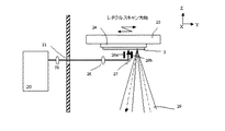
次に第2の実施例を説明する。前述までの実施例では、図2に示すように、パルスレーザーの照射位置31はEUV露光光照射位置32の−Y方向に隣接していた。この構成では、レチクルが+Y方向にスキャンする場合は、露光光照射直前にレチクルにパルスレーザーが照射されるので、仮にパーティクルが付着していたとしても、露光直前に除去され、その状態を維持したまま露光が継続される。しかし、レチクルステージが反転し−Y方向にスキャンする場合は、露光直後にパルスレーザーが照射されるため、反転後にパーティクルが付着した場合、除去を行うことができない構成となっている。
Next, a second embodiment will be described. In the embodiment described above, as shown in FIG. 2, the pulse
本実施例は、この対策として、図8のように、EUV露光光29を挟んで、2箇所にパルスレーザーを照射することを特徴としている。具体的には、入射したパルスレーザー光をハーフミラー27aで50%反射させ、これを一方のパルスビームとし、透過した残り50%をミラー27bで反射させ、これをもう一方の除去パルスビームとする。このような構成とすることで、レチクルスキャンの方向に関わらず、露光直前でレチクル表面にパルスビームを照射することが可能となるため、レチクルステージがスキャン動作を行っている最中にパーティクルが付着しても、すぐさまこれを除去し、レチクルは常に清浄な状態を保つことができる。 The present embodiment is characterized by irradiating a pulse laser at two places with the EUV exposure light 29 sandwiched between them as shown in FIG. More specifically, the incident pulse laser beam is reflected by 50% by the half mirror 27a, which is used as one pulse beam, and the remaining 50% is reflected by the mirror 27b, which is used as the other removal pulse beam. . With this configuration, it is possible to irradiate the reticle surface with a pulse beam immediately before exposure, regardless of the direction of reticle scanning, so that particles adhere while the reticle stage is performing a scanning operation. Even so, it can be removed immediately and the reticle can always be kept clean.
これとまったく同様に、図9に示すように露光光29を挟んで、±Y方向から同時にパルスレーザーを導入し、ミラー27c、27dによって、レチクルにビームを跳ね上げる構成も考えられ、この目的にかなっていれば、どのような構成をとっても構わない。 In exactly the same manner, as shown in FIG. 9, a configuration is also possible in which a pulse laser is introduced simultaneously from the ± Y direction with the exposure light 29 sandwiched, and the beam is jumped to the reticle by mirrors 27c and 27d. Any configuration can be used as long as it is appropriate.
次に第3の実施例を説明する。前述までの実施例では、パルスレーザー照射位置は、EUV露光光照射位置に隣接した位置として説明してきた。本実施例では、図7のように、レチクルステージの加減速領域でパルスレーザーを照射することを特徴とする。レチクルステージは、露光時に所望のスキャン速度(一定速度)を達成するために、等速領域の前後で加減速領域が存在する。前述の実施例の説明でも明らかなように、本来、所定の回路パターン領域を露光する際は、露光直前、すなわち等速領域でパルスレーザー照射を行うのが効果的である。しかし、ステージスキャン速度Vs、パルス繰り返し周波数R、照射パルス数N、シートビーム厚Wには(5)式の関係式があり、それぞれのパラメータは制限を受けるため、所望の除去率を達成したい場合は、レチクルステージ速度を遅くしてパルス数を多くしなければならない可能性もでてくる。この場合、当然スループットが低下してしまうため好ましくない。これの対策として、レチクルステージの加減速領域で、すなわちステージ速度が遅い領域でパルスレーザーを照射することにより、スループットを落とさずにパーティクル除去が可能になる。 Next, a third embodiment will be described. In the embodiments described above, the pulse laser irradiation position has been described as a position adjacent to the EUV exposure light irradiation position. In this embodiment, as shown in FIG. 7, the pulse laser is irradiated in the acceleration / deceleration region of the reticle stage. The reticle stage has acceleration / deceleration areas before and after the constant speed area in order to achieve a desired scanning speed (constant speed) during exposure. As is clear from the description of the above-described embodiment, originally, when exposing a predetermined circuit pattern region, it is effective to perform pulse laser irradiation immediately before exposure, that is, in a constant velocity region. However, the stage scan speed Vs, the pulse repetition frequency R, the number of irradiation pulses N, and the sheet beam thickness W have the relational expression (5), and each parameter is limited, so you want to achieve the desired removal rate There is a possibility that the reticle stage speed must be decreased to increase the number of pulses. In this case, the throughput is naturally reduced, which is not preferable. As a countermeasure against this, it is possible to remove particles without reducing the throughput by irradiating the pulse laser in the acceleration / deceleration region of the reticle stage, that is, in the region where the stage speed is low.
例えば、加減速領域AもしくはBのどちらか一方でパルスレーザー照射を行う場合は、照射ビームは31a、もしくは31bで行うことになり、ステージの往復で2スキャン分除去レーザーが照射されることになる。さらに、加減速領域A,Bの両方で行う場合はレチクルは4スキャン分照射されるため、パーティクルの除去率を鑑みて、どちらかを選択するとよい。このように、レチクルステージの加減速領域では、その速度は等速領域よりも遅いため、パルスレーザーより多く打つことが可能になり、スループットを落とさずにパーティクル除去を良好に行うことが可能になる。 For example, when pulse laser irradiation is performed in either the acceleration / deceleration area A or B, the irradiation beam is performed at 31a or 31b, and the removal laser for two scans is irradiated by reciprocation of the stage. . Furthermore, when performing in both the acceleration / deceleration areas A and B, the reticle is irradiated for four scans, so either one may be selected in view of the particle removal rate. In this way, in the acceleration / deceleration region of the reticle stage, the speed is slower than in the constant velocity region, so that it is possible to hit more than the pulse laser, and it is possible to perform particle removal well without reducing the throughput. .
次に第4の実施例を説明する。前述までの実施例では、除去パルスレーザーの照射形状はレチクルスキャン方向と直交する方向に長いシート状の光ビームであり、これをレチクルのスキャン動作を利用することにより、レチクル前面をレーザー照射することが可能となっていた。この場合、レーザーの照射面積は、シートビーム厚×シートビーム長(例えば、10mm×150mm弱)となり、付着するパーティクルの成分によっては、照射エネルギー密度が低く、所望の除去率を達成できない場合が考えられる。前述のようにパーティクルの付着力は、通常の真空環境下では、Van der Waals力Fvが主なものとされている。この力は、次式でオーダー見積もりが可能である。
Fv=(A*Dp)/(12*Z2) (6)
Next, a fourth embodiment will be described. In the embodiments described above, the irradiation shape of the removal pulse laser is a sheet-like light beam that is long in a direction orthogonal to the reticle scanning direction, and this is used to irradiate the front surface of the reticle with laser by utilizing the reticle scanning operation. Was possible. In this case, the irradiation area of the laser is sheet beam thickness × sheet beam length (for example, less than 10 mm × 150 mm), and depending on the components of the adhered particles, the irradiation energy density may be low and a desired removal rate may not be achieved. It is done. Adhesion of the particles as described above, under normal vacuum environment, Van der Waals force F v is the main thing. This force can be estimated by the following equation.
Fv = (A * Dp) / (12 * Z 2 ) (6)
この式で、Dpはパーティクルの粒径、Zはパーティクル表面と付着平面との距離で通常0.4〜0.5nmとされている。AはHamaker定数といわれるもので、パーティクルの材質によって異なっている。樹脂材料では概略(4〜10)×1E−20J、金属材料では(15〜50)×1E−20Jとなっており、付着するパーティクルの成分によって付着力が異なる。このように、付着力の大きいパーティクルを除去するためには、レチクルのダメージを引き起こさない程度で、照射面積を小さくして、照射エネルギー密度を高くすることが必要になる。 In this equation, Dp is the particle diameter of the particle, and Z is the distance between the particle surface and the adhesion plane, and is usually 0.4 to 0.5 nm. A is referred to as a Hamaker constant, and differs depending on the material of the particles. The resin material is approximately (4 to 10) × 1E-20J, and the metal material is (15 to 50) × 1E-20J, and the adhesion force varies depending on the component of the adhered particles. Thus, in order to remove particles having a large adhesion force, it is necessary to reduce the irradiation area and increase the irradiation energy density to the extent that the reticle is not damaged.
本実施例は、このことに鑑みたもので、照射面積を小さくした場合、除去エリア全面にパルスレーザーを照射するために、図11に示すようにビームをレチクルスキャン方向(Y方向)と直交する方向(X方向)にスキャンする必要性が生ずる。図12はこの目的のために、新たにレーザー光をスキャンするためのポリゴンミラー40と、ビームを集光し、かつ照射エリアのビームスキャン速度を一定にするためのfθレンズ41を設けている。スキャンされたビームはミラー27eで跳ね上げられ、除去エリアに照射される。このときのビームとステージのスキャンの様子を示したものが図10で、本来ビームは連続的にポリゴンミラーにより連続的にスキャンされるが、後の説明のために不連続に示している。本実施例では、ポリゴンミラーでスキャンするので、1方向のみに走査が行われる。例えばビームがある時刻で50の位置にあり、矢印の方向にスキャンされ、51の位置に達すると、すぐさまビームは元の位置に戻る。その間レチクルステージは移動しているので、ビームは52の位置から再びスキャンを開始し、矢印の方向に53の位置まで移動する。このように除去エリア上ではレーザーは斜め方向にスキャン動作を繰り返しながら、除去エリア30をすべてカバーすることになる。
In this embodiment, in view of this, in order to irradiate the entire surface of the removal area with a pulse laser when the irradiation area is reduced, the beam is orthogonal to the reticle scanning direction (Y direction) as shown in FIG. There is a need to scan in the direction (X direction). For this purpose, FIG. 12 is provided with a
この場合も前述の実施例と同様に、有効な除去率を得るために、パルスレーザースキャン長D[mm]、ステージスキャン速度Vs[mm/s]、パルス繰り返し周波数F[Hz]、照射パルス数N[#]、照射エリアW[mm]×W[mm]、ビームスキャン周波数f[Hz]について次のような関係がある。 In this case as well, in order to obtain an effective removal rate, the pulse laser scan length D [mm], the stage scan speed Vs [mm / s], the pulse repetition frequency F [Hz], and the number of irradiation pulses are obtained in the same manner as in the previous embodiment. N [#], irradiation area W [mm] × W [mm], and beam scan frequency f [Hz] have the following relationship.
図11で、パルスレーザースキャン速度をVbとすると、ビームがWだけレーザースキャン方向に移動するのに要する時間△Tsは、
△Ts=W/Vb (7)
である。一方パルスレーザースキャン速度Vbは、除去エリア30のパルスレーザースキャン長をDとすると、1スキャン移動するのに1/fの時間を要するので、Vb=D*f、従って、
△Ts=W/Vb=W/(D*f) (8)
この時間内に移動する照射エリアに対し、最低N回のパルス照射が必要だとすると、このときのパルス時間間隔は、
△Tp=△Ts/N=W/(D*f*N) (9)
となる。一方、パルスレーザー光源のパルス時間間隔△τは、
△τ=1/F (10)
となる。△Tpは、△τよりも大きくなければシステムとして成立しないので、
W/(D*f*N)>1/F (11)
∴(D*f*N)/W<F (12)
というように、パルスレーザーのスキャン方向(X方向)には(12)式の制限がある。
In FIG. 11, when the pulse laser scanning speed is Vb, the time ΔTs required for the beam to move in the laser scanning direction by W is
ΔTs = W / Vb (7)
It is. On the other hand, if the pulse laser scan speed Vb of the
ΔTs = W / Vb = W / (D * f) (8)
Assuming that at least N pulse irradiations are required for the irradiation area moving within this time, the pulse time interval at this time is
ΔTp = ΔTs / N = W / (D * f * N) (9)
It becomes. On the other hand, the pulse time interval Δτ of the pulse laser light source is
Δτ = 1 / F (10)
It becomes. Since ΔTp is not established as a system unless it is larger than Δτ,
W / (D * f * N)> 1 / F (11)
∴ (D * f * N) / W <F (12)
As described above, the scanning direction (X direction) of the pulse laser has a limitation of the expression (12).
また、前述したように、1スキャン終了した後の次のスキャンは、前のスキャンの隣接した位置か、それ以下の位置から始めないと、未照射エリアが生じてしまう。つまり、X方向の1スキャンに要する時間は1/fで、この時間でレチクルステージの移動距離はビームサイズW以内でなければならない。従って、
W>Vs*(1/f) (12)
∴W>Vs*f (13)
というように、レチクルステージのスキャン方向(Y方向)には(13)式の制限がある。
In addition, as described above, an unirradiated area occurs unless the next scan after the end of one scan starts from a position adjacent to or less than the previous scan. That is, the time required for one scan in the X direction is 1 / f, and the movement distance of the reticle stage at this time must be within the beam size W. Therefore,
W> Vs * (1 / f) (12)
∴W> Vs * f (13)
As described above, the scanning direction (Y direction) of the reticle stage is limited by the equation (13).
以上のように、本実施例では、有効な除去率を得るためには、パルスレーザースキャン長D[mm]、ステージスキャン速度Vs[mm/s]、パルス繰り返し周波数F[Hz]、照射パルス数N[#]、照射エリアW[mm]×W[mm]、ビームスキャン周波数f[Hz]について、(11)式、(13)式を同時に満たす必要がある。レーザーのエネルギー密度を大きくするために、照射面積を小さくした場合でも、このようにビームをスキャンする手段を用いることでパーティクルは除去可能になる。なお本実施例では、パルスレーザーのスキャン手段をポリゴンミラーとしたが、ほかのスキャニング手段でも一向に構わない。 As described above, in this embodiment, in order to obtain an effective removal rate, the pulse laser scan length D [mm], the stage scan speed Vs [mm / s], the pulse repetition frequency F [Hz], the number of irradiation pulses For N [#], irradiation area W [mm] × W [mm], and beam scan frequency f [Hz], equations (11) and (13) must be satisfied simultaneously. Even when the irradiation area is reduced in order to increase the energy density of the laser, particles can be removed by using the means for scanning the beam in this way. In this embodiment, the pulse laser scanning means is a polygon mirror, but other scanning means may be used.
次に、第5の実施例について説明する。本発明のパルスレーザー照射によるパーティクル除去法は、パーティクル検査装置でその付着箇所を特定して、その場所にパルスレーザーを照射する方法ではなく、露光装置の露光動作に並行してレチクルの除去エリア全面に除去レーザーを照射する方法をとる。通常、レチクルにはその母材としてゼロデュアなどの超低熱膨張材(例えば熱膨張率0.05E−6/K)が用いられるが、レーザーの長時間に渡る照射によって次第に温度が上昇すると予想される。仮に1℃上昇すると、レチクル全面では約7.5nmの熱膨張となるため、照射エネルギーによっては、レチクルはその場合何らかの発熱対策が必要となる。 Next, a fifth embodiment will be described. The particle removal method by pulse laser irradiation according to the present invention is not a method of identifying the adhesion site with a particle inspection device and irradiating the location with the pulse laser, but in parallel with the exposure operation of the exposure device, the entire area of the reticle removal area Take the method of irradiating the removal laser. Normally, an ultra-low thermal expansion material such as Zerodur (for example, thermal expansion coefficient 0.05E-6 / K) is used as the base material for the reticle, but it is expected that the temperature will gradually increase due to the irradiation of the laser for a long time. . If the temperature rises by 1 ° C., the entire surface of the reticle will have a thermal expansion of about 7.5 nm. Therefore, depending on the irradiation energy, the reticle may need some countermeasure against heat generation.
本実施例は、このことに鑑みたもので、図12にその構成の一例を示す。同図で前述の実施例と比較して新たに加えられた構成が、60a、bのペルチェ素子などの電子冷却手段と、それに接続されている冷却板61a、bである。本実施例では、レチクルの冷却方法として冷却板による輻射冷却を用いる。冷却板としては熱伝導率の高い部材で、輻射率が1に近い大きいもの用いるほうがより効果的である。またサイズと配置に関しては、レチクル全面を覆う大きさに構成し、図のようにレチクル近傍に近接して配置させることで、輻射による冷却方式で重要となる熱源と冷却板との間の形態係数をほぼ1にすることができるため、パルスレーザー照射によって加えられたエネルギーを効率良く回収することが可能となる。本実施例では、冷却方法にペルチェ素子と冷却板を用いた方法について説明したが、ほかの手段、例えば冷却板に冷却水を流して冷却する方法でも良く、効果的に冷却できる方法であればいかなる手段でも構わない。 The present embodiment has been made in view of this, and FIG. 12 shows an example of the configuration. The structure newly added in the same figure compared with the above-mentioned Example is the electronic cooling means, such as 60a, b Peltier elements, and the cooling plates 61a, b connected to it. In this embodiment, radiation cooling by a cooling plate is used as a reticle cooling method. As the cooling plate, it is more effective to use a member having a high thermal conductivity and a radiation rate close to 1. Also, regarding the size and arrangement, it is configured to cover the entire surface of the reticle, and placed close to the reticle as shown in the figure, so that the shape factor between the heat source and the cooling plate, which is important in the cooling method by radiation Therefore, it is possible to efficiently recover the energy applied by the pulse laser irradiation. In this embodiment, a method using a Peltier element and a cooling plate has been described as a cooling method. However, other means, for example, a method of cooling by flowing cooling water through the cooling plate may be used. Any means may be used.
次に、第6の実施例について説明する。前述までの実施例では、パルスレーザー照射によって除去されたパーティクルは、除去後、真空チャンバー内を自由落下して、ほかの部材に衝突、付着すると考えられる。レチクルの下方には投影光学系があるので、反射ミラーなど光学部材の表面に再付着することは反射率の低下や表面の汚染を招く懸念があるため、これを防ぐことが望ましい。本実施例はこのことに鑑みたもので、図13のようにレチクルに入射するパルスレーザーを挟み、かつレチクル近傍に、その間に電場を形成し、パーティクルを捕集する電極28a、bを設けていることを特徴としている。 Next, a sixth embodiment will be described. In the above-described embodiments, it is considered that the particles removed by the pulsed laser irradiation freely fall in the vacuum chamber after the removal, and collide and adhere to other members. Since there is a projection optical system below the reticle, reattachment to the surface of an optical member such as a reflecting mirror may cause a decrease in reflectivity or contamination of the surface, so it is desirable to prevent this. In this embodiment, in view of this, an electrode 28a, b for collecting particles is formed in the vicinity of the reticle by sandwiching a pulse laser incident on the reticle as shown in FIG. It is characterized by being.
パルスレーザーにより除去されたパーティクルが帯電しているかどうかは、明確ではなく、それを測定することも非常に困難であるが、微粒子の帯電に関し、一般的に比較的急激な反応によって生じたものは、帯電粒子を多く含み、穏やかな反応によって作られたものは、帯電していないことが多い、とされている。このことから推察すると、レーザーによって除去されたパーティクルも、ある程度帯電している可能性が高い。そしてその極性は、一般的には、非金属または非金属酸化物の微粒子は正に帯電し、金属または金属酸化物の微粒子は負に帯電するとされている。従って、本実施例のように、28aを+電極、28bを−電極とすることで、パーティクルの材質により帯電極性が異なっていても、電極により捕集可能と考えられる。仮にパーティクルが帯電していない場合でも、電場をかけることで導体の場合は、静電誘導により表面に電荷が生じ、同様に不導体の場合も、誘電分極により表面に電荷が生じ、電場による捕集はある程度可能と考えられる。 It is not clear whether the particles removed by the pulse laser are charged, and it is very difficult to measure them. It is said that a product containing a large amount of charged particles and made by a mild reaction is often not charged. From this, it is highly likely that the particles removed by the laser are also charged to some extent. In general, the polarity of non-metal or non-metal oxide particles is positively charged, and the fine particle of metal or metal oxide is negatively charged. Therefore, as in the present embodiment, by using 28a as a positive electrode and 28b as a negative electrode, even if the charging polarity differs depending on the material of the particles, it can be considered that the electrodes can be collected. Even if the particles are not charged, in the case of a conductor by applying an electric field, a charge is generated on the surface by electrostatic induction. Similarly, in the case of a non-conductor, a charge is generated on the surface by dielectric polarization and is captured by the electric field. Collection is considered possible to some extent.
次に、第7の実施例について説明する。本実施例では、パーティクル除去を効果的に行うために、レチクル多層膜構造に、EUV露光光に対しては透過性があり、パルスレーザー光の波長に対しては吸収する層を1層設けることを特徴とする。パルスレーザー照射により、パーティクルが除去されるメカニズムの一例として、前述もしたがパーティクルと付着表面のnsオーダーの急激な温度上昇による熱膨張によって生ずる加速度が、付着力よりも大きくなるとパーティクルが除去されるとされている。一般的に物質に光が入ったときの透過光量Iは下記のBeerの法則に従う。
I/I0=exp(−α*Z) (14)
Next, a seventh embodiment will be described. In this embodiment, in order to remove particles effectively, the reticle multilayer structure is provided with one layer that is transparent to EUV exposure light and absorbs the wavelength of pulsed laser light. It is characterized by. As an example of the mechanism by which particles are removed by pulse laser irradiation, as described above, the particles are removed when the acceleration caused by the thermal expansion due to the rapid temperature rise of the ns order between the particles and the adhesion surface becomes larger than the adhesion force. It is said that. Generally, the amount of transmitted light I when light enters a material follows the Beer's law below.
I / I 0 = exp (−α * Z) (14)
ここでI0は入射光強度、αは入射光の波長に対する物質吸収係数、Zは物質の厚さである。従って(14)式より吸収係数αが大きいとI/I0は小さくなり、それゆえ物質に吸収される光も多くなり温度が急激に上昇する。一方、吸収係数αが小さいとI/I0は大きくなり、それゆえ吸収される光も小さくなりほとんど温度は上昇しない。 Here, I 0 is the incident light intensity, α is the material absorption coefficient with respect to the wavelength of the incident light, and Z is the thickness of the material. Therefore, if the absorption coefficient α is larger than the equation (14), I / I 0 becomes smaller, and therefore the amount of light absorbed by the substance increases and the temperature rises rapidly. On the other hand, if the absorption coefficient α is small, I / I 0 becomes large, so that the absorbed light becomes small and the temperature hardly rises.
本発明のレチクル多層膜は、図14,15に示すように母材であるゼロデュア60の上層にMo/Siの多層膜61、その上層にEUV露光光は良好に透過し、パルスレーザー光は吸収する熱膨張層62を設ける。除去レーザーをKrFレーザーとすると、この目的にかなった熱膨張層としてSiが挙げられる。この場合、EUV露光光に対してはα=1.7/μm、KrFレーザーに対してはα=166.7/μmとなり、パルスレーザーの入射光を良好に吸収することが可能になる。63は酸化防止用のキャップ層でSiO2等、その上層にバッファー層であるRu層64、その上層にEUV光の吸収層としてCr層65で構成されている。Cr層にパーティクルが付着した場合は、CrはKrFレーザーに対しても吸収を持つので、パーティクルは良好に除去可能である。本実施例では、除去パルスレーザーをKrFレーザー(波長248nm)としたため、それに吸収を持つ物質であるSiを熱膨張層としたが、これ以外にも可能であり、さらにいえば、除去パルスレーザーの波長が異なれば、最適な熱膨張層は他の物質になることは当然である。
In the reticle multilayer film of the present invention, as shown in FIGS. 14 and 15, Mo / Si multilayer film 61 is transmitted in the upper layer of zerodur 60 as a base material, EUV exposure light is transmitted through the upper layer, and pulsed laser light is absorbed. A
(応用例)
次に、上記の露光装置を利用したデバイス製造方法の一例として、半導体デバイスの製造プロセスを説明する。図15は半導体デバイスの全体的な製造プロセスのフローを示す図である。ステップ1(回路設計)では半導体デバイスの回路設計を行う。ステップ2(マスク作製)では設計した回路パターンに基づいてマスクを作製する。一方、ステップ3(ウエハ製造)ではシリコン等の材料を用いてウエハを製造する。ステップ4(ウエハプロセス)は前工程と呼ばれ、上記のマスクとウエハを用いて、上記の露光装置によりリソグラフィ技術を利用してウエハ上に実際の回路を形成する。次のステップ5(組み立て)は後工程と呼ばれ、ステップ5によって作製されたウエハを用いて半導体チップ化する工程であり、アッセンブリ工程(ダイシング、ボンディング)、パッケージング工程(チップ封入)等の組み立て工程を含む。ステップ6(検査)ではステップ5で作製された半導体デバイスの動作確認テスト、耐久性テスト等の検査を行う。こうした工程を経て半導体デバイスが完成し、ステップ7でこれを出荷する。
(Application examples)
Next, a semiconductor device manufacturing process will be described as an example of a device manufacturing method using the above exposure apparatus. FIG. 15 is a diagram showing a flow of an entire manufacturing process of a semiconductor device. In step 1 (circuit design), a semiconductor device circuit is designed. In step 2 (mask fabrication), a mask is fabricated based on the designed circuit pattern. On the other hand, in step 3 (wafer manufacture), a wafer is manufactured using a material such as silicon. Step 4 (wafer process) is called a pre-process, and an actual circuit is formed on the wafer by using the above-described exposure apparatus and lithography technology using the above-described mask and wafer. The next step 5 (assembly) is called a post-process, which is a process for forming a semiconductor chip using the wafer produced in
上記ステップ4のウエハプロセスは以下のステップを有する。ウエハの表面を酸化させる酸化ステップ、ウエハ表面に絶縁膜を成膜するCVDステップ、ウエハ上に電極を蒸着によって形成する電極形成ステップ、ウエハにイオンを打ち込むイオン打ち込みステップ、ウエハに感光剤を塗布するレジスト処理ステップ、上記の露光装置によって回路パターンをレジスト処理ステップ後のウエハに転写する露光ステップ、露光ステップで露光したウエハを現像する現像ステップ、現像ステップで現像したレジスト像以外の部分を削り取るエッチングステップ、エッチングが済んで不要となったレジストを取り除くレジスト剥離ステップ。これらのステップを繰り返し行うことによって、ウエハ上に多重に回路パターンを形成する。 The wafer process in step 4 includes the following steps. An oxidation step for oxidizing the surface of the wafer, a CVD step for forming an insulating film on the wafer surface, an electrode formation step for forming electrodes on the wafer by vapor deposition, an ion implantation step for implanting ions on the wafer, and applying a photosensitive agent to the wafer A resist processing step, an exposure step for transferring the circuit pattern to the wafer after the resist processing step by the above exposure apparatus, a development step for developing the wafer exposed in the exposure step, and an etching step for scraping off portions other than the resist image developed in the development step A resist stripping step that removes the resist that has become unnecessary after etching. By repeating these steps, multiple circuit patterns are formed on the wafer.
以上説明したように、上述の実施例によれば、通常の露光装置の動作シーケンスと同時並行して、パルスレーザー照射によるレチクル上のパーティクル除去を行うため、スループットを低下させることなく、常にレチクル表面を清浄な状態に保った状態で露光を行うことが可能になる。 As described above, according to the above-described embodiment, since the particles on the reticle are removed by pulse laser irradiation in parallel with the operation sequence of the normal exposure apparatus, the reticle surface is always maintained without reducing the throughput. It is possible to perform exposure while maintaining a clean state.
また、上述の実施例によれば、パルスレーザーをシート状に整形し、そのシート幅をレチクルと同程度とし、その方向をレチクルの駆動方向とは直交する方向とすることで、レチクル全面にパルスレーザーを照射することが可能になる。 Further, according to the above-described embodiment, the pulse laser is shaped into a sheet shape, the sheet width is set to the same level as the reticle, and the direction is set to a direction orthogonal to the driving direction of the reticle. It becomes possible to irradiate a laser.
また、上述の実施例によれば、パルスレーザーをスポット状に整形し、そのサイズをパーティクル除去するために必要なエネルギー密度に応じたサイズまで小さくし、なおかつ、レチクルスキャン方向と直交する方向にスポットをスキャンすることで、パーティクル除去に必要なエネルギー密度まで高くして、パルスレーザーをレチクル全面に照射することが可能になる。 In addition, according to the above-described embodiment, the pulse laser is shaped into a spot shape, the size is reduced to a size corresponding to the energy density necessary for particle removal, and the spot is perpendicular to the reticle scan direction. By scanning this, it is possible to increase the energy density necessary for particle removal and irradiate the entire surface of the reticle with a pulse laser.
また、上述の実施例によれば、パルスレーザー照射をレチクルステージが等速運動する前後の加減速運動する領域で行うことで、ステージが低速で駆動しているときに照射が可能になるため、パーティクル除去に必要なパルス数を確保することが可能になる。 In addition, according to the above-described embodiment, by performing pulsed laser irradiation in an acceleration / deceleration movement region before and after the reticle stage moves at a constant speed, irradiation can be performed when the stage is driven at a low speed. It is possible to secure the number of pulses necessary for particle removal.
また、上述の実施例によれば、露光光を挟むように、2箇所でパルスレーザー照射することにより、レチクルの駆動方向に左右されず、露光の直前でパーティクルの除去が可能になる。 Further, according to the above-described embodiment, by irradiating the pulse laser at two locations so as to sandwich the exposure light, it is possible to remove particles immediately before the exposure without depending on the driving direction of the reticle.
また、上述の実施例によれば、レチクルの近傍に輻射冷却手段を設けることで、パーティクル除去用に照射したパルスレーザーによるレチクルの温度上昇を抑えることが可能になる。 Further, according to the above-described embodiment, by providing the radiation cooling means in the vicinity of the reticle, it is possible to suppress the temperature rise of the reticle due to the pulse laser irradiated for particle removal.
また、上述の実施例によれば、レチクルに入射するパルスレーザー光を挟む位置かつレチクルの近傍位置に電極を設け電場を生成することで、除去されたパーティクルが電場により捕集可能になる。 Further, according to the above-described embodiment, the removed particles can be collected by the electric field by generating the electric field by providing the electrode at the position sandwiching the pulse laser beam incident on the reticle and in the vicinity of the reticle.
また、上述の実施例によれば、レチクルを構成している多層膜に、露光光には透過率が高く(吸収係数が小さく)、パルスレーザー光には透過率が低い(吸収係数が大きい)層を有することで、パルスレーザー照射時の表面の温度上昇を大きくさせ、それに伴う熱膨張を大きくさせることで、パーティクルの除去率を向上させることができる。 Further, according to the above-described embodiment, the multilayer film constituting the reticle has high transmittance for exposure light (small absorption coefficient) and low transmittance for pulsed laser light (large absorption coefficient). By having the layer, it is possible to increase the temperature rise of the surface at the time of pulse laser irradiation and increase the thermal expansion associated therewith, thereby improving the particle removal rate.
1 ウエハー
2 レチクル
3、25 レチクルステージ
4 装置チャンバー
5 投影光学系
6 ウエハーステージ
7 装置チャンバー真空ポンプ
8、13 ウエハー搬送ハンド
9 ウエハーロードロックチャンバー真空ポンプ
10 レチクルロードロックチャンバー真空ポンプ
11、16 装置側ゲートバルブ
12、17 ロードロック側ゲートバルブ
18,22 レチクル搬送ハンド
14 ウエハー交換室
19 レチクル交換室
20 パルスレーザー光源
21 パルスレーザー入射窓
22、27b、27c、27d、27e パルスレーザー跳ね上げミラー
24 レチクルホルダー
26 集光光学系
29 EUV露光光
70 整形光学系
30 パーティクル除去エリア
31、31a、31b シート状パルスレーザー光
32 EUV露光光
27a パルスレーザー跳ね上げハーフミラー
40 ポリゴンミラー
41 fθレンズ
50、51、52、53、54、55 パルスレーザースポット
60a,60b ペルチェ素子
61a,61b 輻射冷却板
28a、28b 捕集用電極
60 ゼロデュア
61 Mo/Si多層膜
62 熱膨張層
63 キャップ層
64 バッファー層
65 Cr吸収層
DESCRIPTION OF
Claims (19)
露光用光源からの光により前記原版ステージに保持された原版を照明するための照明光学系と、
前記原版上のパターンを基板に投影するための投影光学系と
を有する露光装置において、
クリーニング用の光を前記原版ステージに保持された原版に照射する照射手段
を有することを特徴とする露光装置。 An original stage holding the original, and
An illumination optical system for illuminating the original held on the original stage by light from an exposure light source;
In an exposure apparatus having a projection optical system for projecting a pattern on the original plate onto a substrate,
An exposure apparatus comprising: irradiation means for irradiating the original held on the original stage with cleaning light.
露光用光源からの光により前記原版ステージに保持された原版を照明するための照明光学系と、
基板を保持し走査方向に移動する基板ステージと、
前記原版上のパターンを前記基板に投影するための投影光学系と
を有する走査露光装置において、
クリーニング用の光を前記原版ステージに保持された原版に照射する照射手段
を有することを特徴とする走査露光装置。 An original stage that holds the original and moves in the scanning direction;
An illumination optical system for illuminating the original held on the original stage by light from an exposure light source;
A substrate stage that holds the substrate and moves in the scanning direction;
In a scanning exposure apparatus having a projection optical system for projecting a pattern on the original plate onto the substrate,
A scanning exposure apparatus comprising: irradiation means for irradiating the original held on the original stage with cleaning light.
(Vs*N)/W<F
なる関係式を満たすように設定されていることを特徴とする請求項7に記載の走査露光装置。 The movement speed Vs of the original stage, the thickness W of the sheet-like beam, the oscillation frequency F of the pulse laser beam, and the number N of irradiation pulses necessary for the cleaning are:
(Vs * N) / W <F
8. The scanning exposure apparatus according to claim 7, wherein the scanning exposure apparatus is set to satisfy the following relational expression.
(D*f*N)/W<F
W>Vs*f
なる2つの関係式を満たすことを特徴とする請求項9に記載の走査露光装置。 The movement speed Vs of the original stage, the spot size W × W, the oscillation frequency F of the pulse laser beam, the number N of irradiation pulses necessary for the cleaning, the scanning length D of the spot, and the scanning frequency f of the spot are:
(D * f * N) / W <F
W> Vs * f
The scanning exposure apparatus according to claim 9, wherein the following two relational expressions are satisfied.
前記投影工程において前記パターンが投影された基板を現像する現像工程と
を有することを特徴とするデバイス製造方法。 A projection step of projecting a pattern on an original onto a substrate using any one of the exposure apparatus according to claim 1 and the scanning exposure apparatus according to claims 2 to 14;
And a development step of developing the substrate on which the pattern is projected in the projection step.
クリーニング用の光を前記原版ステージに保持された原版に照射する照射工程
を有することを特徴とする原版のクリーニング方法。 An original stage for holding an original, an illumination optical system for illuminating the original held on the original stage by light from an exposure light source, and a projection optical system for projecting a pattern on the original onto a substrate A method for cleaning an original plate in an exposure apparatus comprising:
An original plate cleaning method comprising: an irradiation step of irradiating an original plate held on the original plate stage with a cleaning light.
クリーニング用の光を前記原版ステージに保持された原版に照射する照射工程
を有することを特徴とする原版のクリーニング方法。 An original stage that holds the original and moves in the scanning direction, an illumination optical system for illuminating the original held on the original stage by light from an exposure light source, and a substrate stage that holds the substrate and moves in the scanning direction A method for cleaning an original plate in a scanning exposure apparatus having a projection optical system for projecting a pattern on the original plate onto the substrate,
An original plate cleaning method comprising: an irradiation step of irradiating an original plate held on the original plate stage with a cleaning light.
前記多層膜と前記キャップ層との間に、前記露光光に関してよりも前記原版をクリーニングするための光に関して吸収係数が大きい層
を有することを特徴とする原版。 A master plate having a multilayer film that reflects exposure light and a cap layer, the pattern being transferred to the substrate by the exposure light,
An original plate having a layer having a larger absorption coefficient with respect to light for cleaning the original plate than with respect to the exposure light, between the multilayer film and the cap layer.
Priority Applications (2)
| Application Number | Priority Date | Filing Date | Title |
|---|---|---|---|
| JP2004299790A JP2006114650A (en) | 2004-10-14 | 2004-10-14 | Photolithography apparatus, scanning photolithography apparatus, device manufacturing method, original plate cleaning method, and the original plate |
| US11/250,072 US7319507B2 (en) | 2004-10-14 | 2005-10-12 | Apparatus and method for removing contaminant on original, method of manufacturing device, and original |
Applications Claiming Priority (1)
| Application Number | Priority Date | Filing Date | Title |
|---|---|---|---|
| JP2004299790A JP2006114650A (en) | 2004-10-14 | 2004-10-14 | Photolithography apparatus, scanning photolithography apparatus, device manufacturing method, original plate cleaning method, and the original plate |
Publications (2)
| Publication Number | Publication Date |
|---|---|
| JP2006114650A true JP2006114650A (en) | 2006-04-27 |
| JP2006114650A5 JP2006114650A5 (en) | 2007-11-22 |
Family
ID=36180368
Family Applications (1)
| Application Number | Title | Priority Date | Filing Date |
|---|---|---|---|
| JP2004299790A Withdrawn JP2006114650A (en) | 2004-10-14 | 2004-10-14 | Photolithography apparatus, scanning photolithography apparatus, device manufacturing method, original plate cleaning method, and the original plate |
Country Status (2)
| Country | Link |
|---|---|
| US (1) | US7319507B2 (en) |
| JP (1) | JP2006114650A (en) |
Cited By (4)
| Publication number | Priority date | Publication date | Assignee | Title |
|---|---|---|---|---|
| JP2007300096A (en) * | 2006-04-28 | 2007-11-15 | Asml Netherlands Bv | Surface cleaning method, device manufacturing method, cleaning assembly, cleaning apparatus, and lithographic apparatus |
| WO2011016255A1 (en) * | 2009-08-07 | 2011-02-10 | 株式会社ニコン | Exposure apparatus, exposure method, and device manufacturing method |
| JP4761589B1 (en) * | 2010-12-22 | 2011-08-31 | レーザーテック株式会社 | Contamination prevention apparatus, contamination prevention method, exposure apparatus, and patterned wafer manufacturing method |
| JP2015179295A (en) * | 2009-08-07 | 2015-10-08 | 株式会社ニコン | Exposure apparatus and device manufacturing method |
Families Citing this family (6)
| Publication number | Priority date | Publication date | Assignee | Title |
|---|---|---|---|---|
| US7522263B2 (en) * | 2005-12-27 | 2009-04-21 | Asml Netherlands B.V. | Lithographic apparatus and method |
| US20070146658A1 (en) * | 2005-12-27 | 2007-06-28 | Asml Netherlands B.V. | Lithographic apparatus and method |
| JP2008016825A (en) * | 2006-06-09 | 2008-01-24 | Canon Inc | Exposure apparatus, removal method, and device manufacturing method |
| US7903234B2 (en) * | 2006-11-27 | 2011-03-08 | Asml Netherlands B.V. | Lithographic apparatus, device manufacturing method and computer program product |
| US20130235357A1 (en) * | 2012-03-12 | 2013-09-12 | Kla-Tencor Corporation | System and Method for Particle Control Near A Reticle |
| US11687012B2 (en) * | 2021-06-25 | 2023-06-27 | Taiwan Semiconductor Manufacturing Company, Ltd. | Reduce mask defect impact by contamination decompose |
Family Cites Families (9)
| Publication number | Priority date | Publication date | Assignee | Title |
|---|---|---|---|---|
| DE3721940A1 (en) * | 1987-07-02 | 1989-01-12 | Ibm Deutschland | REMOVAL OF PARTICLES FROM SURFACES OF SOLID BODY BY LASER Bombardment |
| JPS6412526U (en) | 1987-07-13 | 1989-01-23 | ||
| JPH10223512A (en) * | 1997-02-10 | 1998-08-21 | Nikon Corp | Electron beam projection aligner |
| EP1011128A4 (en) * | 1997-07-22 | 2004-11-10 | Nikon Corp | Projection exposure method, projection aligner, and methods of manufacturing and optically cleaning the aligner |
| US6385290B1 (en) * | 1998-09-14 | 2002-05-07 | Nikon Corporation | X-ray apparatus |
| JP2000088999A (en) | 1998-09-14 | 2000-03-31 | Nikon Corp | X-ray device |
| DE60118669T2 (en) * | 2000-08-25 | 2007-01-11 | Asml Netherlands B.V. | Lithographic projection apparatus |
| JP3940378B2 (en) * | 2003-05-26 | 2007-07-04 | 沖電気工業株式会社 | Self-cleaning method of semiconductor exposure apparatus and transmission plate for self-cleaning |
| JP2005129898A (en) * | 2003-09-29 | 2005-05-19 | Canon Inc | Aligner and device manufacturing method |
-
2004
- 2004-10-14 JP JP2004299790A patent/JP2006114650A/en not_active Withdrawn
-
2005
- 2005-10-12 US US11/250,072 patent/US7319507B2/en not_active Expired - Fee Related
Cited By (9)
| Publication number | Priority date | Publication date | Assignee | Title |
|---|---|---|---|---|
| JP2007300096A (en) * | 2006-04-28 | 2007-11-15 | Asml Netherlands Bv | Surface cleaning method, device manufacturing method, cleaning assembly, cleaning apparatus, and lithographic apparatus |
| JP4727618B2 (en) * | 2006-04-28 | 2011-07-20 | エーエスエムエル ネザーランズ ビー.ブイ. | Surface cleaning method and apparatus |
| WO2011016255A1 (en) * | 2009-08-07 | 2011-02-10 | 株式会社ニコン | Exposure apparatus, exposure method, and device manufacturing method |
| JP2014207479A (en) * | 2009-08-07 | 2014-10-30 | 株式会社ニコン | Exposure device, exposure method, and device manufacturing method |
| JP5618261B2 (en) * | 2009-08-07 | 2014-11-05 | 株式会社ニコン | Exposure apparatus and device manufacturing method |
| KR101499285B1 (en) * | 2009-08-07 | 2015-03-05 | 가부시키가이샤 니콘 | Exposure apparatus, exposure method, and device manufacturing method |
| JP2015179295A (en) * | 2009-08-07 | 2015-10-08 | 株式会社ニコン | Exposure apparatus and device manufacturing method |
| US9874823B2 (en) | 2009-08-07 | 2018-01-23 | Nikon Corporation | Exposure apparatus, exposure method, and device manufacturing method |
| JP4761589B1 (en) * | 2010-12-22 | 2011-08-31 | レーザーテック株式会社 | Contamination prevention apparatus, contamination prevention method, exposure apparatus, and patterned wafer manufacturing method |
Also Published As
| Publication number | Publication date |
|---|---|
| US20060082743A1 (en) | 2006-04-20 |
| US7319507B2 (en) | 2008-01-15 |
Similar Documents
| Publication | Publication Date | Title |
|---|---|---|
| US7670754B2 (en) | Exposure apparatus having a processing chamber, a vacuum chamber and first and second load lock chambers | |
| US7319507B2 (en) | Apparatus and method for removing contaminant on original, method of manufacturing device, and original | |
| US20100192973A1 (en) | Extreme ultraviolet light source apparatus and cleaning method | |
| US20100183987A1 (en) | Exposure apparatus | |
| KR100563102B1 (en) | A method of cleaning by removing particles from surfaces, a cleaning apparatus and a lithographic projection apparatus | |
| US7379151B2 (en) | Exposure apparatus comprising cleaning apparatus for cleaning mask with laser beam | |
| US20240061325A1 (en) | Euv pellicle and mounting method thereof on photo mask | |
| JP2009146959A (en) | Exposure apparatus, and cleaning device | |
| JP2008147337A (en) | Exposure equipment | |
| US20230341767A1 (en) | Method of fabricating and servicing a photomask | |
| KR100882042B1 (en) | Exposure apparatus, removal method, and device manufacturing method | |
| JP2007329288A (en) | Exposure apparatus, and device manufacturing method | |
| US11385538B2 (en) | Cleaning method for photo masks and apparatus therefor | |
| TWI720574B (en) | Photomask laser etch | |
| US11360384B2 (en) | Method of fabricating and servicing a photomask | |
| JP2008300683A (en) | Cleaning device and method, and exposure apparatus having cleaning device | |
| TWI810829B (en) | Method of manufacturing semiconductor devices using a photomask | |
| KR102613748B1 (en) | Cleaning method for photo masks and apparatus therefor | |
| JP2006120774A (en) | Exposure apparatus and manufacturing method of device |
Legal Events
| Date | Code | Title | Description |
|---|---|---|---|
| A521 | Request for written amendment filed |
Free format text: JAPANESE INTERMEDIATE CODE: A523 Effective date: 20071010 |
|
| A621 | Written request for application examination |
Free format text: JAPANESE INTERMEDIATE CODE: A621 Effective date: 20071010 |
|
| RD04 | Notification of resignation of power of attorney |
Free format text: JAPANESE INTERMEDIATE CODE: A7424 Effective date: 20100201 |
|
| A761 | Written withdrawal of application |
Free format text: JAPANESE INTERMEDIATE CODE: A761 Effective date: 20100217 |