JP2006080509A - Thin substrate support - Google Patents
Thin substrate support Download PDFInfo
- Publication number
- JP2006080509A JP2006080509A JP2005245381A JP2005245381A JP2006080509A JP 2006080509 A JP2006080509 A JP 2006080509A JP 2005245381 A JP2005245381 A JP 2005245381A JP 2005245381 A JP2005245381 A JP 2005245381A JP 2006080509 A JP2006080509 A JP 2006080509A
- Authority
- JP
- Japan
- Prior art keywords
- substrate
- intermediate element
- sample holder
- electrode
- layer
- Prior art date
- Legal status (The legal status is an assumption and is not a legal conclusion. Google has not performed a legal analysis and makes no representation as to the accuracy of the status listed.)
- Pending
Links
- 239000000758 substrate Substances 0.000 title claims abstract description 134
- 239000000463 material Substances 0.000 claims abstract description 52
- 239000004065 semiconductor Substances 0.000 claims abstract description 16
- 238000001816 cooling Methods 0.000 claims abstract description 9
- 238000000034 method Methods 0.000 claims description 22
- 238000012545 processing Methods 0.000 claims description 20
- 229910052782 aluminium Inorganic materials 0.000 claims description 15
- XAGFODPZIPBFFR-UHFFFAOYSA-N aluminium Chemical compound [Al] XAGFODPZIPBFFR-UHFFFAOYSA-N 0.000 claims description 15
- 239000001307 helium Substances 0.000 claims description 14
- 229910052734 helium Inorganic materials 0.000 claims description 14
- SWQJXJOGLNCZEY-UHFFFAOYSA-N helium atom Chemical compound [He] SWQJXJOGLNCZEY-UHFFFAOYSA-N 0.000 claims description 14
- 229910052751 metal Inorganic materials 0.000 claims description 12
- 239000002184 metal Substances 0.000 claims description 12
- RYGMFSIKBFXOCR-UHFFFAOYSA-N Copper Chemical compound [Cu] RYGMFSIKBFXOCR-UHFFFAOYSA-N 0.000 claims description 8
- 229910052802 copper Inorganic materials 0.000 claims description 8
- 239000010949 copper Substances 0.000 claims description 8
- 229920005570 flexible polymer Polymers 0.000 claims description 8
- 229910018072 Al 2 O 3 Inorganic materials 0.000 claims description 6
- TWNQGVIAIRXVLR-UHFFFAOYSA-N oxo(oxoalumanyloxy)alumane Chemical compound O=[Al]O[Al]=O TWNQGVIAIRXVLR-UHFFFAOYSA-N 0.000 claims description 6
- 230000008569 process Effects 0.000 claims description 5
- 239000010410 layer Substances 0.000 description 76
- 239000010453 quartz Substances 0.000 description 9
- VYPSYNLAJGMNEJ-UHFFFAOYSA-N silicon dioxide Inorganic materials O=[Si]=O VYPSYNLAJGMNEJ-UHFFFAOYSA-N 0.000 description 9
- XUIMIQQOPSSXEZ-UHFFFAOYSA-N Silicon Chemical compound [Si] XUIMIQQOPSSXEZ-UHFFFAOYSA-N 0.000 description 7
- 230000009471 action Effects 0.000 description 7
- 239000007789 gas Substances 0.000 description 7
- 238000005530 etching Methods 0.000 description 6
- -1 polytetrafluoroethylene Polymers 0.000 description 6
- 229910052710 silicon Inorganic materials 0.000 description 6
- 239000010703 silicon Substances 0.000 description 6
- 239000004952 Polyamide Substances 0.000 description 5
- 239000004020 conductor Substances 0.000 description 5
- 230000007547 defect Effects 0.000 description 5
- 230000005684 electric field Effects 0.000 description 5
- 229920003023 plastic Polymers 0.000 description 5
- 239000004033 plastic Substances 0.000 description 5
- 229920002647 polyamide Polymers 0.000 description 5
- 230000003068 static effect Effects 0.000 description 5
- 238000012546 transfer Methods 0.000 description 5
- 239000004698 Polyethylene Substances 0.000 description 4
- 239000000919 ceramic Substances 0.000 description 4
- 238000000151 deposition Methods 0.000 description 4
- 229920000573 polyethylene Polymers 0.000 description 4
- 229920000139 polyethylene terephthalate Polymers 0.000 description 4
- 239000005020 polyethylene terephthalate Substances 0.000 description 4
- 229920001343 polytetrafluoroethylene Polymers 0.000 description 4
- 239000004810 polytetrafluoroethylene Substances 0.000 description 4
- 230000008901 benefit Effects 0.000 description 3
- 239000012530 fluid Substances 0.000 description 3
- 239000011810 insulating material Substances 0.000 description 3
- 238000001020 plasma etching Methods 0.000 description 3
- 238000005498 polishing Methods 0.000 description 3
- 229920006254 polymer film Polymers 0.000 description 3
- 239000000853 adhesive Substances 0.000 description 2
- 230000001070 adhesive effect Effects 0.000 description 2
- 239000002998 adhesive polymer Substances 0.000 description 2
- 239000004840 adhesive resin Substances 0.000 description 2
- 229920006223 adhesive resin Polymers 0.000 description 2
- 229910002113 barium titanate Inorganic materials 0.000 description 2
- JRPBQTZRNDNNOP-UHFFFAOYSA-N barium titanate Chemical compound [Ba+2].[Ba+2].[O-][Ti]([O-])([O-])[O-] JRPBQTZRNDNNOP-UHFFFAOYSA-N 0.000 description 2
- 230000015556 catabolic process Effects 0.000 description 2
- 238000005520 cutting process Methods 0.000 description 2
- 239000003989 dielectric material Substances 0.000 description 2
- 238000001312 dry etching Methods 0.000 description 2
- 230000005611 electricity Effects 0.000 description 2
- 150000002500 ions Chemical class 0.000 description 2
- 230000004048 modification Effects 0.000 description 2
- 238000012986 modification Methods 0.000 description 2
- 238000009832 plasma treatment Methods 0.000 description 2
- 239000004800 polyvinyl chloride Substances 0.000 description 2
- 229920005989 resin Polymers 0.000 description 2
- 239000011347 resin Substances 0.000 description 2
- 239000002470 thermal conductor Substances 0.000 description 2
- PXGOKWXKJXAPGV-UHFFFAOYSA-N Fluorine Chemical compound FF PXGOKWXKJXAPGV-UHFFFAOYSA-N 0.000 description 1
- 229910004298 SiO 2 Inorganic materials 0.000 description 1
- GWEVSGVZZGPLCZ-UHFFFAOYSA-N Titan oxide Chemical compound O=[Ti]=O GWEVSGVZZGPLCZ-UHFFFAOYSA-N 0.000 description 1
- 229910021417 amorphous silicon Inorganic materials 0.000 description 1
- 238000007743 anodising Methods 0.000 description 1
- 229910052454 barium strontium titanate Inorganic materials 0.000 description 1
- 230000004888 barrier function Effects 0.000 description 1
- 239000005388 borosilicate glass Substances 0.000 description 1
- 238000005219 brazing Methods 0.000 description 1
- 150000001768 cations Chemical class 0.000 description 1
- 238000004891 communication Methods 0.000 description 1
- 239000013078 crystal Substances 0.000 description 1
- 238000000354 decomposition reaction Methods 0.000 description 1
- 230000008021 deposition Effects 0.000 description 1
- 230000002542 deteriorative effect Effects 0.000 description 1
- 238000005516 engineering process Methods 0.000 description 1
- 229920006332 epoxy adhesive Polymers 0.000 description 1
- 229910052731 fluorine Inorganic materials 0.000 description 1
- 239000011737 fluorine Substances 0.000 description 1
- 239000011521 glass Substances 0.000 description 1
- 239000004519 grease Substances 0.000 description 1
- 238000000227 grinding Methods 0.000 description 1
- 239000011261 inert gas Substances 0.000 description 1
- 238000002955 isolation Methods 0.000 description 1
- 238000005304 joining Methods 0.000 description 1
- 239000002346 layers by function Substances 0.000 description 1
- 238000004519 manufacturing process Methods 0.000 description 1
- 238000004806 packaging method and process Methods 0.000 description 1
- 230000002093 peripheral effect Effects 0.000 description 1
- 230000035699 permeability Effects 0.000 description 1
- 238000000206 photolithography Methods 0.000 description 1
- 229920003223 poly(pyromellitimide-1,4-diphenyl ether) Polymers 0.000 description 1
- 230000001681 protective effect Effects 0.000 description 1
- 230000005855 radiation Effects 0.000 description 1
- 230000002441 reversible effect Effects 0.000 description 1
- 238000000926 separation method Methods 0.000 description 1
- 239000002904 solvent Substances 0.000 description 1
- VEALVRVVWBQVSL-UHFFFAOYSA-N strontium titanate Chemical compound [Sr+2].[O-][Ti]([O-])=O VEALVRVVWBQVSL-UHFFFAOYSA-N 0.000 description 1
- 239000000126 substance Substances 0.000 description 1
- 239000002344 surface layer Substances 0.000 description 1
- OGIDPMRJRNCKJF-UHFFFAOYSA-N titanium oxide Inorganic materials [Ti]=O OGIDPMRJRNCKJF-UHFFFAOYSA-N 0.000 description 1
- 238000003466 welding Methods 0.000 description 1
Images


Classifications
-
- H—ELECTRICITY
- H01—ELECTRIC ELEMENTS
- H01L—SEMICONDUCTOR DEVICES NOT COVERED BY CLASS H10
- H01L21/00—Processes or apparatus adapted for the manufacture or treatment of semiconductor or solid state devices or of parts thereof
- H01L21/67—Apparatus specially adapted for handling semiconductor or electric solid state devices during manufacture or treatment thereof; Apparatus specially adapted for handling wafers during manufacture or treatment of semiconductor or electric solid state devices or components ; Apparatus not specifically provided for elsewhere
- H01L21/683—Apparatus specially adapted for handling semiconductor or electric solid state devices during manufacture or treatment thereof; Apparatus specially adapted for handling wafers during manufacture or treatment of semiconductor or electric solid state devices or components ; Apparatus not specifically provided for elsewhere for supporting or gripping
- H01L21/6831—Apparatus specially adapted for handling semiconductor or electric solid state devices during manufacture or treatment thereof; Apparatus specially adapted for handling wafers during manufacture or treatment of semiconductor or electric solid state devices or components ; Apparatus not specifically provided for elsewhere for supporting or gripping using electrostatic chucks
Abstract
Description
本発明は2004年9月8日に出願された仏国特許出願第0451992号に基づき、その開示全体を本願明細書に援用し、本願明細書にその優先権を主張する。
本発明は半導体基板のプラズマ処理に関し、特にエッチングおよび/またはプラズマ堆積に関する。本発明はより正確には、厚さ500μm未満の基板用の支持体に関する。
The present invention is based on the French patent application No. 0451992 filed on Sep. 8, 2004, the entire disclosure of which is hereby incorporated by reference and claims the priority thereof.
The present invention relates to plasma processing of semiconductor substrates, and more particularly to etching and / or plasma deposition. The present invention more precisely relates to a support for a substrate having a thickness of less than 500 μm.
半導体産業では、ウエハ形態の基板の操作は製造工程の重要な性格を表す。厚い半導体基板ウエハ、例えば、シリコンウエハ上に集積回路を製造した後、このウエハは機械的作用によってその用途に必要な厚さに薄くされなければならない。 In the semiconductor industry, the manipulation of wafer-type substrates represents an important feature of the manufacturing process. After the integrated circuit is fabricated on a thick semiconductor substrate wafer, such as a silicon wafer, the wafer must be thinned to the thickness required for the application by mechanical action.
この薄くすることは次の2つの結果を生む:
a)薄くされる前には剛性であった基板を約100μm以下に薄くすると、撓み易くなり、操作が非常に困難になる。
b)機械的作用によって材料の構造が10μm〜30μmの深さに変わる。すなわち、単結晶であった基板の構造が非結晶質になる。したがって、次にこの層を除去するために、薄くされた基板を処理しなければならない。
This thinning has two consequences:
a) If the substrate, which was rigid before being thinned, is thinned to about 100 μm or less, it becomes easy to bend and the operation becomes very difficult.
b) The structure of the material changes to a depth of 10 μm to 30 μm by mechanical action. That is, the structure of the substrate that was a single crystal becomes amorphous. Therefore, the thinned substrate must then be processed to remove this layer.
先行技術のある薄くする方法では、集積回路が製造されたウエハの前面はプラスチック材料でのフィルムで被覆される。次に、このウエハはその後面に機械的作用を加えることにより薄くする研磨機に導入される。次に、薄くされたウエハは第2の処理を受けて薄くすることによって改変された表面層を、機械的または化学的研磨によって除去する。 In one prior art thinning method, the front surface of the wafer on which the integrated circuit is manufactured is coated with a film of plastic material. The wafer is then introduced into a polisher that thins it by applying mechanical action to its rear surface. The thinned wafer is then subjected to a second treatment to remove the surface layer that has been modified by thinning by mechanical or chemical polishing.
上記2工程の後、半導体基板の薄くされた面は、金属フレームによって支持されたプラスチック材料のフィルムから成る支持体に固定される。次に、このプラスチック材料のフィルムが基板の前面から除去される。次に、支持されたフィルム/基板アセンブリは鋸盤に導入され、そこで切断ラインのすべてを通過しながら鋸歯が基板の厚さ全体を貫通して、まだプラスチック材料のフィルムに固定されている回路を個々に分離する。次に、支持されたフィルム/基板アセンブリが鋸盤から取り外され、回路はそれぞれのパッケージング内に搭載される準備ができる。この方法の大きな欠点は回路のエッジ部にシリコンの削片が発生することにある。鋸刃によって作られるこれらの削片は、回路を破壊することもある欠陥の原因である。 After the above two steps, the thinned surface of the semiconductor substrate is fixed to a support made of a film of plastic material supported by a metal frame. The plastic material film is then removed from the front surface of the substrate. The supported film / substrate assembly is then introduced into the saw machine where the saw blade penetrates the entire thickness of the substrate while passing through all of the cutting lines, and the circuit is still secured to the plastic material film. Separate individually. The supported film / substrate assembly is then removed from the saw and the circuit is ready to be mounted in the respective packaging. The major disadvantage of this method is that silicon chips are generated at the edge of the circuit. These pieces created by the saw blade are the cause of defects that can destroy the circuit.
ダイシングバイグラインディング(DBG)またはダイシングバイシニング(DBT)として知られている上記方法の変形例は、鋸歯により生じる欠陥の数を低減させるが、完全には除去しない。薄くする操作の前に、厚い半導体基板ウエハはその前面から部分的に切断され、鋸歯は基板の最終的な厚さより僅かに大きい深さまで基板を貫通するだけである。次に、ウエハの前面が保護的なプラスチック材料のフィルムで被覆され、厚いウエハは研磨機に導入されて、鋸の底が切断するまで、機械的作用によってその中で薄くされる。したがって、回路が分離されて、薄くされた基板ウエハの形態を取り、非結晶質になった層を除去するために後から機械的または化学的に研磨される。 A variation of the above method known as dicing big grinding (DBG) or dicing bicing (DBT) reduces the number of defects caused by saw teeth, but does not completely eliminate them. Prior to the thinning operation, the thick semiconductor substrate wafer is partially cut from its front surface and the saw blades only penetrate the substrate to a depth slightly greater than the final thickness of the substrate. Next, the front surface of the wafer is coated with a film of protective plastic material and the thick wafer is introduced into the polisher and thinned therein by mechanical action until the bottom of the saw is cut. Thus, the circuitry is separated and takes the form of a thinned substrate wafer that is later mechanically or chemically polished to remove the amorphous layer.
この後、回路の機械的分離に用いた鋸に代えて、回路の間の溝をマシニングまたはプラズマエッチングする新しい技術が導入された。プラズマエッチングは物理化学的現象によって材料を除去することを伴う作用であるので、機械的原因による欠陥を生じるリスクはない。したがって、この操作から生じる欠陥は最小になる。有利にはプラズマエッチングが、薄くすることの前後に回路を分離するための鋸歯の代わりとなるかもしれず、研磨による薄くされた後に非結晶化したシリコンの層を除去するための研磨技術の代わりにもなるかもしれない。 Later, instead of the saw used for mechanical isolation of circuits, new techniques were introduced to machine or plasma etch grooves between circuits. Since plasma etching is an action that involves removing material by a physicochemical phenomenon, there is no risk of causing defects due to mechanical causes. Therefore, the defects resulting from this operation are minimized. Advantageously, plasma etching may be an alternative to saw blades to isolate the circuit before and after thinning, and instead of a polishing technique to remove a layer of amorphous silicon after being thinned by polishing. May also be.
プラズマエッチング技術では、フォトリソグラフィの工程が半導体基板の面の1つに適用され、これによってプラズマに晒される領域、故にエッチングされる領域が定められ、その他の領域が感光性樹脂マスクによってプラズマから保護される。半導体基板はエンクロージャ内に設置されたサンプルホルダ上に置かれる。プラズマはこのエンクロージャ内で例えばSF6などのフッ素を含んだ低圧ガスを用いて生成される。同時に、サンプルホルダは負に分極されて陽イオンによる基板表面のボンバードメントを加速するので、材料のエッチングが加速されるとともにエッチングの垂直度が強調される。 In plasma etching technology, a photolithography process is applied to one of the surfaces of the semiconductor substrate, thereby defining the areas exposed to the plasma and hence the areas to be etched, and the other areas are protected from the plasma by the photosensitive resin mask. Is done. The semiconductor substrate is placed on a sample holder installed in the enclosure. Plasma is generated using a low-pressure gas containing fluorine such as for example SF 6 within the enclosure. At the same time, the sample holder is negatively polarized to accelerate the bombardment of the substrate surface by cations, so that the etching of the material is accelerated and the perpendicularity of the etching is emphasized.
エッチング中、基板は熱に晒されて、その表面温度が上昇する。感光性樹脂のエッチングマスクおよび基板内に存在する電子回路を損傷しないように、エッチング操作を通して基板を冷却してその温度を80℃〜100℃以下の値に維持しなければならない。基板を冷却するために、基板は機械的または静電的手段によって、冷却システムを備えたサンプルホルダの表面に接触した状態に保たれ、ヘリウムガスがサンプルホルダの上面と基板の下面との間に注入される。このガスは基板からサンプルホルダに熱を伝達する。 During etching, the substrate is exposed to heat and its surface temperature rises. In order not to damage the photosensitive resin etching mask and the electronic circuits present in the substrate, the substrate must be cooled through the etching operation to maintain its temperature at a value between 80 ° C. and 100 ° C. To cool the substrate, the substrate is kept in contact with the surface of the sample holder with the cooling system by mechanical or electrostatic means, and helium gas is placed between the upper surface of the sample holder and the lower surface of the substrate. Injected. This gas transfers heat from the substrate to the sample holder.
熱的に効果的であるように、ヘリウムの圧力は約10mbarより大きくなければならない。厚い基板の場合、この圧力は問題を生じさせないが、特に個々の回路から構成されているときには薄くされた基板ウエハを変形させ易い。したがって、薄くされた後、剛性支持体に基板ウエハを反転可能に固定することが不可欠である。 To be thermally effective, the pressure of helium must be greater than about 10 mbar. In the case of thick substrates, this pressure does not cause a problem, but it tends to deform a thinned substrate wafer, especially when it is made up of individual circuits. Therefore, after thinning, it is essential to fix the substrate wafer to the rigid support in a reversible manner.
第1の技術は粘着性ポリマーフィルムを用いて薄くされた基板ウエハを剛性支持体に固定することに存する。 The first technique consists in fixing a substrate wafer thinned with an adhesive polymer film to a rigid support.
高温に晒されるとその接着性が失われる特性を有する(熱テープとして知られている)フィルムを用いて、標準的な厚さの半導体基板に薄くされた基板を固定することが示唆され、これは個々の回路の摘み取りを可能にするはずである。実際、一旦加熱されたフィルムは薄いシリコンの機械的強度よりも大きな接着性を保持するので、個々の回路を完全に破壊せずに、その支持体から個々の回路を分離することは極めて困難である。 It is suggested to fix a thinned substrate to a standard thickness semiconductor substrate using a film (known as thermal tape) that has the property that its adhesion is lost when exposed to high temperatures. Should allow picking of individual circuits. In fact, once heated, the film retains greater adhesion than the mechanical strength of thin silicon, making it very difficult to separate individual circuits from their support without completely destroying the individual circuits. is there.
石英を通して紫外線が照射されるとその接着性が失われる特性を有する(UVテープとして知られている)フィルムを用いて、厚さ約1mmの石英の剛性片に薄くされた基板を固定することも想定されてきた。この技術には大きな2つの欠点がある。第1に、シリコン(156W/m.K)に比して、石英は非常に劣る(1W/m.K)熱導体である。したがって、その熱抵抗は非常に高く、シリコン基板の表面はすぐに80℃〜100℃を超える温度に達する。唯一の解決策はエッチング速度を遅くすることであるが、これは生産性を低下させる。また、石英は電気的に絶縁性があり、このことは基板が静電的手段によってサンプルホルダ上に保持され得ないことを意味する。 Using a film (known as UV tape) that loses its adhesion when irradiated with ultraviolet light through quartz, the thinned substrate can be fixed to a rigid piece of quartz about 1 mm thick. It has been assumed. This technique has two major drawbacks. First, compared to silicon (156 W / m.K), quartz is a very poor (1 W / m.K) thermal conductor. Therefore, its thermal resistance is very high, and the surface of the silicon substrate quickly reaches a temperature exceeding 80 ° C. to 100 ° C. The only solution is to slow the etch rate, but this reduces productivity. Quartz is also electrically insulative, meaning that the substrate cannot be held on the sample holder by electrostatic means.
第2の技術は静電的手段によって薄くされた基板ウエハを可動支持体に固定することにある。 The second technique is to fix a substrate wafer thinned by electrostatic means to a movable support.
米国特許出願第2002/110449号明細書は、工程中および工程段階の間に基板がそこに固定されたままになる搬送可能な支持体上に基板を保持することを提案している。この支持体は石英、ガラス、アルミニウム、または酸化チタンなどのセラミックおよびチタン酸バリウムの形態の誘電材料を含む。この支持体は静電力を発生する電荷を生成かつ蓄積させる電気回路を組み込む。 U.S. Patent Application No. 2002/110449 proposes holding a substrate on a transportable support where the substrate remains secured during and during the process. The support comprises a ceramic such as quartz, glass, aluminum or titanium oxide and a dielectric material in the form of barium titanate. The support incorporates an electrical circuit that generates and stores charge that generates electrostatic forces.
このシステムには大きな2つの欠点がある。第1に、厚さ0.3mm〜2.5mmのセラミックは熱抵抗が高い。機械的手段を用いてサンプルホルダ上に搬送可能な支持体を保持する場合、ヘリウムの圧力が薄いセラミックの中央を変形させる。この変形によって熱伝達が不均一になり(熱はその中央にさらに伝わる)、この変形を被るシリコン基板を劣化させるリスクが極めて高くなる。 This system has two major drawbacks. First, a ceramic having a thickness of 0.3 mm to 2.5 mm has a high thermal resistance. When holding a transportable support on the sample holder using mechanical means, the center of the ceramic with the thin helium pressure is deformed. Due to this deformation, heat transfer becomes non-uniform (heat is further transferred to the center), and the risk of deteriorating the silicon substrate subjected to this deformation becomes extremely high.
この後、電極は次の工程の前に荷電されるので、電極に蓄積された電荷が操作中にその中に残っている場合に限り、静電的システムは動作することができる。プラズマ媒質を用いた真空でドライエッチングを行い、かつ30kHz〜13.56MHzの周波数で基板の極性を交番する操作の現状では、永久的には付勢されない電極は放電して、基板を保持する静電力が失われるかもしれない。 After this, the electrode is charged before the next step, so that the electrostatic system can only operate if the charge accumulated on the electrode remains in it during operation. In the current situation of performing dry etching in a vacuum using a plasma medium and alternating the polarity of the substrate at a frequency of 30 kHz to 13.56 MHz, the electrode that is not permanently energized is discharged, and a static electricity is held to hold the substrate. Electricity may be lost.
米国特許第出願2004/037692号明細書は、(例えば、その後面に金属を堆積させるか、またはベースに基板を溶接する)基板の温度が400℃を超え得る間に基板の処理に耐えることが意図された可動基板ホルダを記載している。この基板ホルダは、好適には絶縁材料(SiO2、Si3N4)の層で被覆された熱伝導率が著しくは高くはないセラミック半導体材料(ALO2、カプトン、SiC)から成るベースを含む。高温で使用されるように設計されたこの基板ホルダは、基板を効果的に冷却して80℃以下の温度に維持することができない。 US Patent Application No. 2004/037692 is able to withstand processing of a substrate while the temperature of the substrate can exceed 400 ° C. (eg, by depositing metal on its back side or welding the substrate to the base). An intended movable substrate holder is described. The substrate holder is preferably includes a base made of an insulating material (SiO 2, Si 3 N 4 ) ceramic semiconductor material coated thermal conductivity layer is not higher significantly in (ALO2, Kapton, SiC). This substrate holder, designed to be used at high temperatures, cannot effectively cool the substrate and maintain it at temperatures below 80 ° C.
また、基板は処理中に外部からの付勢を必要としない静電的システムによって基板ホルダ上に保持される。このシステムは可動イオンを含む材料(ホウケイ酸ガラス)または高い誘電率を有する材料(チタン酸バリウムまたはチタン酸ストロンチウム)の機能層に配置された金属電極から構成される。基板を固定するために、電圧が2本の電極の端子に印加される。可動イオンは印加された電界によって移動され、個々の電気的双極子を生成する。この双極子によって生じた個々の電界の合計は、電圧が除去された後に残存する高い電界を発生する。処理中に基板ホルダ上に基板を保持するのは、この残留電界である。 The substrate is also held on the substrate holder by an electrostatic system that does not require external bias during processing. This system consists of a metal electrode arranged in a functional layer of a material containing mobile ions (borosilicate glass) or a material with a high dielectric constant (barium titanate or strontium titanate). In order to fix the substrate, a voltage is applied to the terminals of the two electrodes. Mobile ions are moved by an applied electric field, generating individual electrical dipoles. The sum of the individual electric fields produced by this dipole generates a high electric field that remains after the voltage is removed. It is this residual electric field that holds the substrate on the substrate holder during processing.
プラズマ媒質を用いた真空でドライエッチングを行い、かつ30kHz〜13.56MHzの周波数で基板の極性を交番する操作の現状では、この解決策は使用され得ない。これは交流電圧の作用が、電気的双極子を反転させて、基板を固定している電界を無効にするので、基板ホルダ上に基板を保持することができないためである。 This solution cannot be used in the current situation of dry etching in a vacuum using a plasma medium and alternating the polarity of the substrate at a frequency of 30 kHz to 13.56 MHz. This is because the action of the AC voltage inverts the electric dipole and invalidates the electric field fixing the substrate, so that the substrate cannot be held on the substrate holder.
米国特許第6268994号明細書はサンプルを支持するように適合されたチャック(chuck)を開示しており、これは冷却システムを備え、導電性ベースのオリフィスに挿入されるボルトによって共に留められた導電性ベースおよびフレームである2つの部分から構成されている。この2つの部分は電気的かつ熱的に接続される。導電性ベースとフレームとの接合はエポキシ接着剤、熱伝導性グリス、またはろう付けによって行われ得る。サンプルは第1の絶縁層、導電層、および第2の絶縁層により連続的に被覆された導電性部分から成るベースに静電的に固定される。このチャックは薄いかもしくは壊れやすいサンプルの捜査の問題を解決していない。
本発明は、先行技術のデバイスの欠点を有さず、かつプラズマ媒質を用いた真空においてその処理のために薄い半導体基板ウエハを支持するように適合されたデバイスを提案する。特に、本発明のデバイスは、基板に取り付けられ、かつ容易に操作できるようにするために該基板から取外し可能な基板用の剛性支持体を提供する。さらに、本発明のデバイスは処理中に基板の温度を80℃以下に保持することができる。最終的に、本発明のデバイスは処理後に基板の容易かつ全体的な解放を可能にするはずであり、妥当な場合には切断して回路を形成することも可能にするはずである。 The present invention proposes a device that does not have the disadvantages of prior art devices and is adapted to support a thin semiconductor substrate wafer for its processing in a vacuum using a plasma medium. In particular, the device of the present invention provides a rigid support for a substrate that is attached to the substrate and removable from the substrate for easy operation. Furthermore, the device of the present invention can keep the temperature of the substrate below 80 ° C. during processing. Ultimately, the device of the present invention should allow easy and total release of the substrate after processing and should also allow cutting to form a circuit if appropriate.
本発明は半導体基板を支持するデバイスに存し、本デバイスは冷却システムおよび電気的接続手段を含んだ処理室に取り付けられたサンプルホルダを備え、本デバイスは静電的手段によって、またはクランプを用いてサンプルホルダに固定されるとともに電気的かつ熱的にサンプルホルダに接続された中間要素をさらに備えており、該中間要素は取外し可能であり、それが支持する薄い基板の操作を可能にするのに十分な剛性を有し、かつ
基板よりも高い導電率を有する第1の材料から成るベースと、
ベースを被覆しかつ高い誘電強度を有する第2の材料から成る第1の層と、
第1の層上に配設された第1および第2の電極と、
第1の層および電極を被覆しかつ高い誘電強度を有する第3の材料から成る第2の層とを含む。
The present invention resides in a device for supporting a semiconductor substrate, the device comprising a sample holder attached to a processing chamber containing a cooling system and electrical connection means, the device by electrostatic means or using a clamp Further comprising an intermediate element fixed to the sample holder and electrically and thermally connected to the sample holder, the intermediate element being removable, allowing manipulation of the thin substrate it supports A base made of a first material having a sufficient rigidity and having a higher conductivity than the substrate;
A first layer comprising a second material covering the base and having a high dielectric strength;
First and second electrodes disposed on the first layer;
And a second layer made of a third material covering the electrode and having a high dielectric strength.
中間要素は取外し可能であり、それが支持する薄い基板の操作を可能にするのに十分な剛性を有する。 The intermediate element is removable and has sufficient rigidity to allow manipulation of the thin substrate it supports.
本発明のデバイスは有利には、中間要素および薄い基板を組み合せたものを何回もサンプルホルダに固定することを可能にし、基板単独の場合と同じオーダーの大きさである組み合せたものをそこから分離することを可能にする。本発明は改変していない標準的な装置(ロボットアーム、室扉、基板ホルダ、搬送カセット等)を使用できるようにし、合理的な漏れ量で中間要素の下にヘリウムを注入することに存する従来の冷却システムを用いて中間要素を冷却する。 The device of the invention advantageously makes it possible to fix the combination of the intermediate element and the thin substrate to the sample holder many times, from which the combination is of the same order of magnitude as the substrate alone. Makes it possible to separate. The present invention allows the use of standard equipment (robot arms, chamber doors, substrate holders, transfer cassettes, etc.) that is not modified and injects helium under the intermediate element with a reasonable amount of leakage. The intermediate element is cooled using a cooling system.
上記方法で得られた中間要素−基板アセンブリは、薄くする前の基板だけの大きさとほぼ同じ寸法、すなわち直径150mm〜200mm、薄くする前の基板の大きさとほぼ同じ厚さ、および500g未満の重量を有する。この中間要素−基板アセンブリは軽量で、容易に搬送可能であり、薄くされた基板を損傷させることはない。 The intermediate element-substrate assembly obtained by the above method has approximately the same dimensions as the size of the substrate before thinning, that is, 150 mm to 200 mm in diameter, approximately the same thickness as the substrate before thinning, and a weight of less than 500 g. Have This intermediate element-substrate assembly is lightweight, easily transportable and does not damage the thinned substrate.
中間要素のベースを構成する材料は、基板のプラズマ処理によって生成される熱を冷却されたサンプルホルダに容易に排出できるように、基板よりも一層高い熱伝導率を、好適にはできるだけ高い熱伝導率を有していなければならない。本発明の第1の実施形態では、第1の材料は金属であり、好適には銅またはアルミニウムである。 The material constituting the base of the intermediate element has a higher thermal conductivity than the substrate, preferably as high as possible, so that the heat generated by the plasma treatment of the substrate can be easily discharged to a cooled sample holder. Must have a rate. In the first embodiment of the present invention, the first material is a metal, preferably copper or aluminum.
誘電材料の第1の層はベースから電極を絶縁する。この材料は数kVの破壊電圧を生じずに、耐える能力がなければならない。第1の層を構成するこの材料は基板と中間要素のベースとの間に熱障壁を生じないように、できるだけ高い熱伝導率も有さなければならない。当然、可能であれば、このような2つの基準は同時に最適化されなければならない。第2の実施形態では、第2の材料は酸化アルミニウムAl2O3、例えば、ベースの表面または電極の表面に形成されたアノード処理されたアルミの層であり、これはどちらがアルミニウムで製造されているかによる。 The first layer of dielectric material insulates the electrode from the base. This material must be capable of withstanding without producing a breakdown voltage of several kV. This material constituting the first layer must also have as high a thermal conductivity as possible so as not to create a thermal barrier between the substrate and the base of the intermediate element. Of course, if possible, these two criteria should be optimized simultaneously. In the second embodiment, the second material is aluminum oxide Al 2 O 3 , for example a layer of anodized aluminum formed on the surface of the base or the surface of the electrode, which is made of aluminum. It depends on what you do.
この第1の絶縁層は電極と接触している。電極は、例えば、特に第1の絶縁層の上に導電性材料を堆積させることによって得られる導電性材料の薄層の形態であってよい。第3の実施形態では、電極は金属、好適には銅またはアルミニウムである。 The first insulating layer is in contact with the electrode. The electrode may be, for example, in the form of a thin layer of conductive material obtained, in particular, by depositing a conductive material on the first insulating layer. In a third embodiment, the electrode is a metal, preferably copper or aluminum.
この電極は、数kVの破壊電圧を起こさずに抵抗する能力があり、かつ基板を冷却するのに役立つように非常に良好な熱の伝導体である第2の絶縁層で被覆される。この第2の絶縁層に選択した材料は、第1の絶縁層の材料に適用する基準と同様の電気的および熱的基準を満たさなければならない。しかし、この材料はプラズマの分解作用に局所的に晒されるので、交換および除去が容易になり得る材料を使用することが有利である。第4の実施形態では、第3の材料は可撓性ポリマーである。一変形例では、可撓性ポリマーは粘着性樹脂である。別の変形例では、可撓性ポリマーはポリテトラフルオロエチレン(PTFE)、ポリ塩化ビニル(PVC)、ポリエチレン(PE)、およびポリアミド(PA)から選択される。 This electrode is coated with a second insulating layer which is capable of resisting without causing a breakdown voltage of several kV and is a very good thermal conductor to help cool the substrate. The material selected for this second insulating layer must meet electrical and thermal criteria similar to those applied to the material of the first insulating layer. However, it is advantageous to use a material that can be easily replaced and removed, since this material is locally exposed to the decomposition action of the plasma. In a fourth embodiment, the third material is a flexible polymer. In one variation, the flexible polymer is an adhesive resin. In another variation, the flexible polymer is selected from polytetrafluoroethylene (PTFE), polyvinyl chloride (PVC), polyethylene (PE), and polyamide (PA).
第2の絶縁層は、例えば好ましくは電極と接触する側に接着性のあるポリマーフィルム、またはスピナを用いて堆積され得、かつ適した溶剤、例えばポリアミドを用いて化学的に除去され得る材料から構成されてよい。この絶縁層の上面の表面が、それが支持する薄い基板に応力を生じないように完全に平坦になっていることも重要である。 The second insulating layer may be deposited from a material that can be deposited, for example, using an adhesive polymer film or spinner, preferably on the side in contact with the electrode, and chemically removed using a suitable solvent, such as polyamide. May be configured. It is also important that the top surface of this insulating layer be completely flat so as not to stress the thin substrate it supports.
本発明のデバイスは多数の利点を有する。第1に、中間要素は石英と比べて安価なアルミニウムディスクなどの材料から作製され得る。第2に、石英を損傷させかつその透過性の一部を損なわせる引っかき傷などの欠陥の影響を受け難い。第3に、紫外線に反応し易い石英およびフィルムの場合、本デバイスは化学線作用のない光線などの特別な環境を必要としない。最後に、磨耗が生じた場合、上部の誘電体、特にそれがポリマーフィルムであるか、またはスピナを用いて堆積されている場合には交換が非常に簡単である。 The device of the present invention has a number of advantages. First, the intermediate element can be made from a material such as an aluminum disk that is less expensive than quartz. Second, it is less susceptible to defects such as scratches that damage quartz and impair some of its permeability. Third, in the case of quartz and films that are sensitive to ultraviolet light, the device does not require a special environment such as light without actinic radiation. Finally, if wear occurs, replacement is very simple if the top dielectric, especially if it is a polymer film or is deposited using a spinner.
本発明の一実施形態では、基板は静電的手段によって中間要素に固定され、かつ中間要素は静電的手段によってサンプルホルダに固定される。サンプルホルダは電極を含み、中間要素が電圧を印加した結果生じる静電圧によってサンプルホルダに対して保持されるように、数kVの電圧が該電極の間に印加される。静電的手段によってサンプルホルダに中間要素を固定する方法は、上記のような中間要素に基板を固定する方法に類似する。中間要素がサンプルホルダに対して保持されるように、電極の間に数kVの電圧が印加される。 In one embodiment of the invention, the substrate is secured to the intermediate element by electrostatic means, and the intermediate element is secured to the sample holder by electrostatic means. The sample holder includes electrodes, and a voltage of several kV is applied between the electrodes so that the intermediate element is held against the sample holder by a static voltage that results from applying the voltage. The method of fixing the intermediate element to the sample holder by electrostatic means is similar to the method of fixing the substrate to the intermediate element as described above. A voltage of several kV is applied between the electrodes so that the intermediate element is held against the sample holder.
この場合、中間要素は直径が基板の寸法とほぼ同じ大きさであるディスクであることが好ましい。 In this case, the intermediate element is preferably a disk whose diameter is approximately the same as the dimensions of the substrate.
別の実施形態では、基板は静電的手段によって中間要素に固定され、中間要素はクランプを用いてサンプルホルダに固定される。「クランプ」という用語は、中間部材に力を及ぼし、かつサンプルホルダ上に中間部材を押圧する作用を有し、この力を無効にすることによってサンプルホルダから中間要素を簡単に分離することを可能にする任意の固定手段を意味する。この種の固定手段は、特に欧州特許第1263025号明細書に記載されている。 In another embodiment, the substrate is secured to the intermediate element by electrostatic means, and the intermediate element is secured to the sample holder using a clamp. The term “clamp” acts to exert a force on the intermediate member and press the intermediate member onto the sample holder, allowing the intermediate element to be easily separated from the sample holder by disabling this force Means any fixing means. Such a fixing means is described in particular in EP 1 263 025.
この実施形態では、中間要素はクランプの支持領域を提供するように直径が基板の寸法よりも僅かに大きいディスクである。 In this embodiment, the intermediate element is a disk whose diameter is slightly larger than the dimensions of the substrate so as to provide a support area for the clamp.
この場合、前記ベースはクランプの顎部の間にそれを把持できるように少なくとも1mm、より好適には1mm〜2mmの厚さを有することが好ましい。 In this case, the base preferably has a thickness of at least 1 mm, more preferably 1 mm to 2 mm so that it can be gripped between the jaws of the clamp.
本発明の第1の態様によれば、加圧ヘリウムのフィルムが中間要素とサンプルホルダとの間に形成される。熱交換を可能にする不活性ガスとして用いられるヘリウムの流れは、このガスを用いてそれを一掃して恒久的なガスのフィルムを形成するために、サンプルホルダの上面および中間要素の下面と反対に導かれる。 According to a first aspect of the invention, a pressurized helium film is formed between the intermediate element and the sample holder. The flow of helium used as an inert gas that allows heat exchange is opposite to the upper surface of the sample holder and the lower surface of the intermediate element in order to sweep it away to form a permanent gas film. Led to.
本発明の第2の態様によれば、加圧ヘリウムのフィルムは中間要素と基板との間に形成される。ヘリウムは中間要素の上面と基板の下面との間にも導入される。 According to a second aspect of the invention, a film of pressurized helium is formed between the intermediate element and the substrate. Helium is also introduced between the upper surface of the intermediate element and the lower surface of the substrate.
効果的な熱移動を提供するために、ヘリウム圧は少なくとも10mbarでなければならない。 In order to provide effective heat transfer, the helium pressure must be at least 10 mbar.
このプラズマはガス状で導電性の媒質であるので、ガスが導入されるとすぐに静電圧が再び確立される。この静電圧のために、シリコン基板は中間要素に対して押圧され、その表面に生じた熱は最適な条件下で排出される。この処理の最後には、ガスおよびプラズマの導入が停止され、中間要素の接点から電圧が除去される。次に、この薄い基板を保持している中間要素がこの装置から取り出される。 Since this plasma is a gaseous and conductive medium, the static voltage is established again as soon as the gas is introduced. Due to this static voltage, the silicon substrate is pressed against the intermediate element and the heat generated on its surface is discharged under optimal conditions. At the end of this process, the introduction of gas and plasma is stopped and the voltage is removed from the contacts of the intermediate element. The intermediate element holding the thin substrate is then removed from the apparatus.
必要であれば、中間−基板アセンブリは装置の外部で、基板を保持するのに用いられる電圧と逆符号の電圧がその間に印加される2つの電気接点を備えた、サンプルホルダと同様の部材上に設置されてよい。この段階では基板は完全に解放されており、次の工程の用意ができている。 If necessary, the intermediate-substrate assembly is external to the device, on a member similar to the sample holder, with two electrical contacts between which a voltage of the opposite sign to that used to hold the substrate is applied. It may be installed in. At this stage, the substrate is completely released and the next process is ready.
本発明の特定の一実施形態では、第1の電極は実質的にディスク状であり、第2の電極は第1の電極を囲繞する実質的にリング状である。サンプルホルダとの電気的導通を確立するために、電極の各々は、中間要素のベースからそれを絶縁するために第1の層で被覆された個々の延長部を含み、ベースを貫いてベースの後面まで通って2つの電気的接点を形成する。このプラズマ処理装置の外部で、基板はサンプルホルダの電気接点と向かい合う2つの電気接点を備えた中間要素上に設置される。数kVの電圧が2本の電極間に数分間印加される。次に、基板は電圧を印加することにより生じる静電圧によって中間部材に保持される。次に、この中間要素−基板アセンブリは装置に挿入され、静電圧によって、または開けるのが簡単なクランプを用いて、サンプルホルダに固定される。サンプルホルダ上に設置されるとすぐに、電気的導通が中間要素の接点とサンプルホルダの接点との間に確立され、数kVの電圧が電極間に確立される。 In one particular embodiment of the invention, the first electrode is substantially disk-shaped and the second electrode is substantially ring-shaped surrounding the first electrode. In order to establish electrical communication with the sample holder, each of the electrodes includes an individual extension coated with a first layer to insulate it from the base of the intermediate element, through the base Two electrical contacts are formed through to the rear surface. Outside the plasma processing apparatus, the substrate is placed on an intermediate element with two electrical contacts facing the electrical contacts of the sample holder. A voltage of several kV is applied between the two electrodes for several minutes. Next, the substrate is held on the intermediate member by a static voltage generated by applying a voltage. This intermediate element-substrate assembly is then inserted into the apparatus and secured to the sample holder by means of an electrostatic voltage or using a clamp that is easy to open. As soon as it is placed on the sample holder, electrical continuity is established between the contact of the intermediate element and the contact of the sample holder, and a voltage of several kV is established between the electrodes.
本発明の別の実施形態では、中間要素は、
高い誘電強度を有する第4の材料から構成され、かつ第1の層の反対側にあるベースを被覆する第3の層と、
該第3の層上に配設された第3および第4の電極と、
高い誘電強度を有する第5の材料から構成され、かつ第3の層ならびに第3および第4の電極を被覆する第4の層とを含む。
In another embodiment of the invention, the intermediate element is
A third layer made of a fourth material having a high dielectric strength and covering the base on the opposite side of the first layer;
Third and fourth electrodes disposed on the third layer;
A fourth layer made of a fifth material having a high dielectric strength and covering the third layer and the third and fourth electrodes.
この第3の絶縁層はベースの反対側にある第1の絶縁層と同じ機能、すなわちベースから電極を電気的に絶縁する機能を有する。したがって、第4の材料は第1の絶縁層を構成する第2の材料の特性と類似する特性を有していなければならない。第4の材料は、酸化アルミニウムAl2O3、例えば、ベースの表面または電極の表面に形成されたアノード処理されたアルミの層であることが好ましく、これはベースか電極のうちのどれがアルミニウムで製造されているかによる。 This third insulating layer has the same function as the first insulating layer on the opposite side of the base, that is, the function of electrically insulating the electrode from the base. Therefore, the fourth material must have characteristics similar to those of the second material constituting the first insulating layer. The fourth material is preferably aluminum oxide Al 2 O 3 , for example a layer of anodized aluminum formed on the surface of the base or the surface of the electrode, which is either aluminum or aluminum Depending on whether it is manufactured in
例えば、第3および第4の電極は、特に第3の絶縁層の上に導電性材料を堆積させることによって得られる導電性材料の薄層の形態であってよい。この電極は金属、好適には銅またはアルミニウムである。 For example, the third and fourth electrodes may be in the form of a thin layer of conductive material, particularly obtained by depositing a conductive material over the third insulating layer. This electrode is a metal, preferably copper or aluminum.
第4の絶縁層はベースの反対側にある第2の絶縁層と同じ機能を有する。したがって、第5の材料は第2の絶縁層を構成する第3の材料の特性と類似する特性を有していなければならない。第2の材料は可撓性ポリマーであることが好ましい。可撓性ポリマーの一変形例は粘着性樹脂である。別の変形例では、可撓性ポリマーはポリテトラフルオロエチレン(PTFE)、ポリ塩化ビニル(PVC)、ポリエチレン(PE)、およびポリアミド(PA)から選択される。 The fourth insulating layer has the same function as the second insulating layer on the opposite side of the base. Therefore, the fifth material must have characteristics similar to those of the third material constituting the second insulating layer. The second material is preferably a flexible polymer. One variation of the flexible polymer is an adhesive resin. In another variation, the flexible polymer is selected from polytetrafluoroethylene (PTFE), polyvinyl chloride (PVC), polyethylene (PE), and polyamide (PA).
本発明の特定の一実施形態では、第3の電極は実質的にはディスク状であり、第4の電極は実質的には第3の電極を囲繞するリング状である。サンプルホルダとの電気的導通を確立するために、各電極はベースから電極を中間要素のベースから絶縁するために第3の層で被覆された個々の延長部を含み、ベースを貫いてベースの後面まで通って2つの電気的接点を形成する。第3の電極の延長部は有利には第1の電極の延長部と共通であり、第4の電極の延長部は有利には第2の電極の延長部と共通である。このように、中間要素がサンプルホルダと電気的に接触するのは2点だけである。 In one particular embodiment of the invention, the third electrode is substantially disk-shaped and the fourth electrode is substantially ring-shaped surrounding the third electrode. To establish electrical continuity with the sample holder, each electrode includes an individual extension coated with a third layer to insulate the electrode from the base from the base of the intermediate element, through the base Two electrical contacts are formed through to the rear surface. The extension of the third electrode is preferably the same as the extension of the first electrode, and the extension of the fourth electrode is preferably the same as the extension of the second electrode. Thus, there are only two points where the intermediate element is in electrical contact with the sample holder.
本発明は上記のようなデバイスを用いて半導体基板を操作する方法をさらに提供する。この方法は、
静電的手段によって基板を中間要素に固定する工程、
基板を保持する中間要素を処理室に導入する工程、
処理室に取り付けられ、かつ冷却システムおよび中間要素と電気的に接続するための手段を備えたサンプルホルダに、中間要素を固定する工程、
プラズマ媒質を用いて真空で基板を処理する工程、
処理した基板を保持する中間要素からサンプルホルダを取り外す工程、
中間要素から基板を取り外す工程を含む。
The present invention further provides a method of manipulating a semiconductor substrate using a device as described above. This method
Fixing the substrate to the intermediate element by electrostatic means;
Introducing an intermediate element for holding the substrate into the processing chamber;
Securing the intermediate element to a sample holder attached to the processing chamber and provided with means for electrically connecting the cooling system and the intermediate element;
Processing the substrate in a vacuum using a plasma medium;
Removing the sample holder from the intermediate element holding the treated substrate;
Removing the substrate from the intermediate element.
中間要素はサンプルホルダに静電的に固定されることが好ましい。中間要素がサンプルホルダに対して保持されるように、数kVの電圧が電極間に印加される。中間要素はクランプを用いてサンプルホルダに固定されてもよい。 The intermediate element is preferably electrostatically fixed to the sample holder. A voltage of several kV is applied between the electrodes so that the intermediate element is held against the sample holder. The intermediate element may be fixed to the sample holder using a clamp.
本発明は処理速度の点で最適な条件下で基板に損傷を及ぼすことなく薄い基板のプラズマ処理を可能にするという利点を有する。第一に、高速の処理を可能にすると同時に、基板の温度は約80℃以下の値に保持され得る。第二に、分離後、これによって分離された回路を楽に取り上げることが可能となるので、損傷は生じない。最後に、温度または紫外線に反応し易いフィルムを用いて薄くした基板を石英支持体に固定する方法とは異なり、基板はプラズマ処理の前または後で危険な操作に晒されない。 The present invention has the advantage of allowing plasma processing of thin substrates without damaging the substrate under conditions optimal in terms of processing speed. First, the temperature of the substrate can be kept at a value of about 80 ° C. or less while allowing high speed processing. Second, after the separation, the separated circuit can be easily picked up, so that no damage occurs. Finally, unlike the method of fixing a thinned substrate to a quartz support using a film that is sensitive to temperature or ultraviolet light, the substrate is not exposed to dangerous operations before or after plasma processing.
本発明の他の特徴および利点は、非限定的な例として示した以下の実施形態の説明の過程および添付図面において明白となろう。 Other features and advantages of the present invention will become apparent in the course of the following description of the embodiments given as a non-limiting example and in the accompanying drawings.
図1に示したように、本発明のデバイスは、処理室に取り付けられ冷却システムを備えたサンプルホルダ1を備えており、この冷却システムは熱交換流体を供給するとともに該流体を例えば熱交換デバイスに排出する管2およびこの流体用の通路3を含んでいる。中間要素5aに固定された基板4がサンプルホルダ1上に設置されている。ヘリウムなどの不活性熱交換ガスがサンプルホルダ1の上面と中間要素5aの下面との間および基板4の下面と中間要素5aの上面との間に注入されて薄層6を形成する。
As shown in FIG. 1, the device of the present invention includes a sample holder 1 attached to a processing chamber and provided with a cooling system, which supplies a heat exchange fluid and supplies the fluid, for example, a heat exchange device. A
ここではディスク状である中間要素5aは、金属、例えば銅(熱係数Cth=401W/m.K)またはアルミニウム(Cth=237W/m.K)などの非常に良好な熱の導体である材料から成るベース7を含んでいる。ベース7を構成するこの材料の熱伝導率は、プラズマ処理によって基板4に発生した熱をヘリウム層6に伝えるために、高くなければならず、基板4の熱伝導率よりも一層高くなければならない。
The intermediate element 5a, here in the form of a disk, is a very good heat conductor such as a metal, for example copper (thermal coefficient C th = 401 W / m.K) or aluminum (C th = 237 W / m.K). A
ベース7はアルミニウムであることが好ましい。基板を受け取ることになっている側にあるベース7の面7aは、高い誘電強度を有する絶縁性材料、例えば酸化アルミニウムAl2O3の層8で被覆される。この絶縁層は、特にベース7の上面のアルミニウムをアノード処理することによって得られ得る。層8は電極を構成する導電層9で被覆される。層8の機能は導電層9からベース7の材料を電気的に絶縁することである。不連続な導電層9は厚さが数μmであり、銅の層であることが好ましい。導電層9は2本の同心電極を含み、中心ディスク9aの形状を有する一方の電極はリング9bの形状を有する第2の電極によって囲繞されている。導電層9は層8によってベース7から電気的に絶縁された2つの延長部9cを有している。すなわち、一方は中心ディスク9aに延び、他方は周縁部でリング9bに延びている。このような延長部9cは中間要素5aの後面に現れて2つの電気的接点領域10を形成する。一旦中間要素5aがサンプルホルダ1上に設置されると、この領域10は、サンプルホルダ1から現れるそれに対応する2つの電気的接続部11と接触して、電極9aと9bとの間に電圧を印加できるようにする。
The
導電層9は高い誘電強度を有する材料の第2の絶縁層12によって保護される。この例では、導電層9の上面と接触するその下方側で接着性のある厚さが70μm〜170μmのポリエチレンテレフタレート(PET)のフィルムが使用される。
The conductive layer 9 is protected by a second insulating
この実施形態では、中間要素5aは基板4と同じ直径Dを有する。ベース7およびこれを被覆する各層8、9、12は同じ直径Dを有する。中間要素5aは、基板4が中間要素5aに固定されるのと同じ方法で、サンプルホルダ1に組み込まれた電極(図示せず)を用いた静電的手段によってサンプルホルダ1に固定されてよい。
In this embodiment, the intermediate element 5 a has the same diameter D as the substrate 4. The
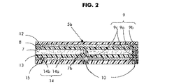
図2は先の実施形態の変形例に相当する中間要素5bを示している。第3の絶縁層13が、基板の反対側にあり、かつ第1の絶縁層8によって被覆されていない側にあるベース7の面7b上に堆積される。絶縁層13は層8の特性と類似する特性を有する。これは高い誘電強度を有する絶縁性材料、例えば酸化アルミニウムAl2O3から構成される。
FIG. 2 shows an intermediate element 5b corresponding to a modification of the previous embodiment. A third insulating
厚さ数μmであり、好適には銅である不連続な導電層14が絶縁層13上に堆積される。導電層14は2本の同心電極を含み、中心ディスク14aの形状を有する一方の電極はリング14bの形状を有する第2の電極によって囲繞されている。電極14aおよび14bは電極9aおよび9bの延長部にそれぞれ電気的に接続されており、接点領域10を介して中間要素から現れる。
A discontinuous
導電層14は高い誘電強度を有する材料の第4の絶縁層15によって保護される。第2の層12と同様、導電層14の上面と接触するその下方側で接着性のある絶縁層15は厚さが70μm〜170μmのポリエチレンテレフタレート(PET)フィルムから構成され得る。
The
この実施形態では、中間要素5bは基板4と同じ直径Dを有する。ベース7およびこれを被覆する各層13、14、15は同じ直径Dを有する。中間要素5bは、中間要素5bに組み込まれた電極14aおよび14bを使用する静電的手段により、これらもまた中間要素5bに組み込まれている電極9aおよび9bによる静電的手段によって基板4が中間要素5bに固定されるのと同じ方法で、サンプルホルダ1に固定されてよい。
In this embodiment, the intermediate element 5 b has the same diameter D as the substrate 4. The
図3に示した本発明の実施形態では、図1に示したものと同様の要素には同じ参照番号で示している。この実施形態はクランプによってサンプルホルダ1に固定できるように中間要素25が基板4の直径よりも大きい直径D’を有しているという点で図1の実施形態とは異なっている。この固定形態は、特に欧州特許第1263025号明細書に記載されている。ベース27および第1の絶縁層28は要素25と同じ直径D’を有する。導電層9および第2の絶縁層12は基板4と同じ直径Dを有する。したがって、第1の絶縁層28は直径の差を補償するために、その周縁部において層9および12の厚さの合計に等しい厚さが増大した部分28aを有する。サンプルホルダ1に要素25を固定する手段は、この厚さが増大した部分28aに影響する。
In the embodiment of the present invention shown in FIG. 3, elements similar to those shown in FIG. This embodiment differs from the embodiment of FIG. 1 in that the
1 サンプルホルダ
3 通路
4 基板
5a、25 中間要素
6 ヘリウム層
7 ベース
7a 面
8 Al2O3層
9、14 導電層
9a、9b、14 電極
9c 延長部
10 電気的接点領域
11 電気的接続部
12、13、15、18、28 絶縁層
14a 電極
1
Claims (26)
前記基板よりも高い導電率を有する第1の材料から成るベースと、
前記ベースを被覆しかつ高い誘電強度を有する第2の材料から成る第1の層と、
前記第1の層上に配設された第1および第2の電極と、
前記第1の層および前記電極を被覆しかつ高い誘電強度を有する第3の材料から成る第2の層とを含んだデバイス。 A device for supporting a semiconductor substrate comprising a sample holder attached to a processing chamber containing a cooling system and electrical connection means, said device holding said sample holder by electrostatic means or using a clamp And an intermediate element that is fixed to the sample holder and electrically and thermally connected to the sample holder, the intermediate element being removable and rigid enough to allow manipulation of the thin substrate it supports And a base made of a first material having a higher conductivity than the substrate;
A first layer comprising a second material covering the base and having a high dielectric strength;
First and second electrodes disposed on the first layer;
A device comprising: the first layer; and a second layer made of a third material covering the electrode and having a high dielectric strength.
高い誘電強度を有する第4の材料から構成され、かつ前記第1の層の反対側にある前記ベースを被覆する第3の層と、
前記第3の層上に配設された第3および第4の電極と、
前記第3の層ならびに前記第3および第4の電極を被覆し、かつ高い誘電強度を有する第5の材料から構成された第4の層とを含む請求項14に記載のデバイス。 The intermediate element is
A third layer made of a fourth material having a high dielectric strength and covering the base on the opposite side of the first layer;
Third and fourth electrodes disposed on the third layer;
The device according to claim 14, further comprising: a fourth layer made of a fifth material covering the third layer and the third and fourth electrodes and having a high dielectric strength.
静電的手段によって前記基板を中間要素に固定する工程と、
前記基板を保持する前記中間要素を処理室に導入する工程と、
前記処理室に取り付けられ、かつ冷却システムおよび前記中間要素と電気的に接続する手段を備えたサンプルホルダに、前記中間要素を固定する工程と、
プラズマ媒質を用いて真空で前記基板を処理する工程と、
処理した基板を保持する前記中間要素から前記サンプルホルダを取り外す工程と、
前記中間要素から前記基板を取り外す工程とを含む半導体基板を操作する方法。 A method of manipulating a semiconductor substrate using the device of claim 1, comprising:
Fixing the substrate to the intermediate element by electrostatic means;
Introducing the intermediate element holding the substrate into a processing chamber;
Securing the intermediate element to a sample holder attached to the process chamber and provided with a cooling system and means for electrical connection with the intermediate element;
Processing the substrate in a vacuum using a plasma medium;
Removing the sample holder from the intermediate element holding the treated substrate;
Removing the substrate from the intermediate element.
Applications Claiming Priority (1)
| Application Number | Priority Date | Filing Date | Title |
|---|---|---|---|
| FR0451992A FR2875054B1 (en) | 2004-09-08 | 2004-09-08 | THIN SUBSTRATES SUPPORT |
Publications (1)
| Publication Number | Publication Date |
|---|---|
| JP2006080509A true JP2006080509A (en) | 2006-03-23 |
Family
ID=34951024
Family Applications (1)
| Application Number | Title | Priority Date | Filing Date |
|---|---|---|---|
| JP2005245381A Pending JP2006080509A (en) | 2004-09-08 | 2005-08-26 | Thin substrate support |
Country Status (5)
| Country | Link |
|---|---|
| US (1) | US20060051893A1 (en) |
| EP (1) | EP1635381A3 (en) |
| JP (1) | JP2006080509A (en) |
| CN (1) | CN1747145A (en) |
| FR (1) | FR2875054B1 (en) |
Cited By (2)
| Publication number | Priority date | Publication date | Assignee | Title |
|---|---|---|---|---|
| JP2016510168A (en) * | 2013-02-14 | 2016-04-04 | プラズマ − サーム、エルエルシー | Method and apparatus for plasma dicing a semiconductor wafer |
| JP2019522374A (en) * | 2016-07-22 | 2019-08-08 | アプライド マテリアルズ インコーポレイテッドApplied Materials,Incorporated | Processed wafers as workpiece carrier tops in semiconductor and machine processing |
Families Citing this family (6)
| Publication number | Priority date | Publication date | Assignee | Title |
|---|---|---|---|---|
| US8726838B2 (en) * | 2010-03-31 | 2014-05-20 | Intermolecular, Inc. | Combinatorial plasma enhanced deposition and etch techniques |
| JP5807160B2 (en) * | 2012-12-13 | 2015-11-10 | パナソニックIpマネジメント株式会社 | Non-plasma dry etching equipment |
| JP5621142B2 (en) * | 2013-04-02 | 2014-11-05 | 独立行政法人産業技術総合研究所 | Semiconductor process carrier |
| US20160141318A1 (en) * | 2013-06-28 | 2016-05-19 | Teledyne Dalsa, Inc. | Method and system for assembly of radiological imaging sensor |
| US20180122679A1 (en) * | 2016-10-28 | 2018-05-03 | Applied Materials, Inc. | Stress balanced electrostatic substrate carrier with contacts |
| CN113058767B (en) * | 2021-03-05 | 2022-05-31 | Tcl华星光电技术有限公司 | Support column and alignment mechanism |
Citations (10)
| Publication number | Priority date | Publication date | Assignee | Title |
|---|---|---|---|---|
| JPH05198663A (en) * | 1992-01-21 | 1993-08-06 | Hitachi Ltd | Sample conveying holder |
| JPH0774234A (en) * | 1993-06-28 | 1995-03-17 | Tokyo Electron Ltd | Electrode structure of electrostatic chuck, its assembly method, its assembly jig and treatment apparatus |
| JPH07130828A (en) * | 1993-10-28 | 1995-05-19 | Sony Corp | Semiconductor manufacturing apparatus |
| JPH0917849A (en) * | 1995-06-28 | 1997-01-17 | Ngk Insulators Ltd | Semiconductor wafer holding device, its manufacture and its use method |
| JPH09162272A (en) * | 1995-12-04 | 1997-06-20 | Sony Corp | Electrostatic chuck, thin board holding device, semiconductor manufacturing device, and transfer method |
| JPH10189697A (en) * | 1996-12-26 | 1998-07-21 | Kyocera Corp | Electrostatic chuck device |
| JPH10209257A (en) * | 1997-01-22 | 1998-08-07 | Tomoegawa Paper Co Ltd | Electrostatic chuck device and its manufacture |
| JP2003100856A (en) * | 2001-09-26 | 2003-04-04 | Kyocera Corp | Wafer supporting member |
| JP2003179127A (en) * | 2001-12-11 | 2003-06-27 | Taiheiyo Cement Corp | Power feed terminal of an electrostatic chuck |
| JP2004111533A (en) * | 2002-09-17 | 2004-04-08 | Tokyo Electron Ltd | Electrostatic attraction apparatus |
Family Cites Families (8)
| Publication number | Priority date | Publication date | Assignee | Title |
|---|---|---|---|---|
| KR100264445B1 (en) * | 1993-10-04 | 2000-11-01 | 히가시 데쓰로 | Plasma treatment equipment |
| US5463525A (en) * | 1993-12-20 | 1995-10-31 | International Business Machines Corporation | Guard ring electrostatic chuck |
| US6268994B1 (en) * | 1999-07-09 | 2001-07-31 | Dorsey Gage, Inc. | Electrostatic chuck and method of manufacture |
| US7027283B2 (en) | 2000-08-02 | 2006-04-11 | Fraunhofer-Gesellschaft Zur Foerderung Der Angewandten Forschung E.V. | Mobile holder for a wafer |
| EP1217655A1 (en) * | 2000-12-23 | 2002-06-26 | VenTec Gesellschaft für Venturekapital und Unternehmensberatung | Method of handling a thin wafer |
| DE60106577T8 (en) | 2001-05-31 | 2006-04-27 | Alcatel | Removable umbrella device for plasma reactors |
| EP1359466A1 (en) * | 2002-05-01 | 2003-11-05 | ASML Netherlands B.V. | Chuck, lithographic projection apparatus, method of manufacturing a chuck and device manufacturing method |
| EP1458019A3 (en) * | 2003-03-13 | 2005-12-28 | VenTec Gesellschaft für Venturekapital und Unternehmensberatung | Mobile transportable electrostatic substrate holders |
-
2004
- 2004-09-08 FR FR0451992A patent/FR2875054B1/en active Active
-
2005
- 2005-08-17 EP EP05107567A patent/EP1635381A3/en not_active Withdrawn
- 2005-08-26 JP JP2005245381A patent/JP2006080509A/en active Pending
- 2005-09-07 US US11/219,651 patent/US20060051893A1/en not_active Abandoned
- 2005-09-07 CN CN200510098329.7A patent/CN1747145A/en active Pending
Patent Citations (10)
| Publication number | Priority date | Publication date | Assignee | Title |
|---|---|---|---|---|
| JPH05198663A (en) * | 1992-01-21 | 1993-08-06 | Hitachi Ltd | Sample conveying holder |
| JPH0774234A (en) * | 1993-06-28 | 1995-03-17 | Tokyo Electron Ltd | Electrode structure of electrostatic chuck, its assembly method, its assembly jig and treatment apparatus |
| JPH07130828A (en) * | 1993-10-28 | 1995-05-19 | Sony Corp | Semiconductor manufacturing apparatus |
| JPH0917849A (en) * | 1995-06-28 | 1997-01-17 | Ngk Insulators Ltd | Semiconductor wafer holding device, its manufacture and its use method |
| JPH09162272A (en) * | 1995-12-04 | 1997-06-20 | Sony Corp | Electrostatic chuck, thin board holding device, semiconductor manufacturing device, and transfer method |
| JPH10189697A (en) * | 1996-12-26 | 1998-07-21 | Kyocera Corp | Electrostatic chuck device |
| JPH10209257A (en) * | 1997-01-22 | 1998-08-07 | Tomoegawa Paper Co Ltd | Electrostatic chuck device and its manufacture |
| JP2003100856A (en) * | 2001-09-26 | 2003-04-04 | Kyocera Corp | Wafer supporting member |
| JP2003179127A (en) * | 2001-12-11 | 2003-06-27 | Taiheiyo Cement Corp | Power feed terminal of an electrostatic chuck |
| JP2004111533A (en) * | 2002-09-17 | 2004-04-08 | Tokyo Electron Ltd | Electrostatic attraction apparatus |
Cited By (2)
| Publication number | Priority date | Publication date | Assignee | Title |
|---|---|---|---|---|
| JP2016510168A (en) * | 2013-02-14 | 2016-04-04 | プラズマ − サーム、エルエルシー | Method and apparatus for plasma dicing a semiconductor wafer |
| JP2019522374A (en) * | 2016-07-22 | 2019-08-08 | アプライド マテリアルズ インコーポレイテッドApplied Materials,Incorporated | Processed wafers as workpiece carrier tops in semiconductor and machine processing |
Also Published As
| Publication number | Publication date |
|---|---|
| FR2875054A1 (en) | 2006-03-10 |
| EP1635381A2 (en) | 2006-03-15 |
| EP1635381A3 (en) | 2008-10-15 |
| FR2875054B1 (en) | 2006-12-01 |
| CN1747145A (en) | 2006-03-15 |
| US20060051893A1 (en) | 2006-03-09 |
Similar Documents
| Publication | Publication Date | Title |
|---|---|---|
| CN101405857B (en) | Apparatus and method for carrying substrates | |
| JP2006080509A (en) | Thin substrate support | |
| JP4942471B2 (en) | Susceptor and wafer processing method using the same | |
| US8879233B2 (en) | Electrostatic chuck with polymer protrusions | |
| US7655579B2 (en) | Method for improving heat transfer of a focus ring to a target substrate mounting device | |
| US7667945B2 (en) | Bipolar carrier wafer and mobile bipolar electrostatic wafer arrangement | |
| EP1662559B1 (en) | Method of processing objects comprising a surface portion made of an insulator | |
| US7192841B2 (en) | Method of wafer/substrate bonding | |
| IE52318B1 (en) | Method and apparatus for dry etching and electrostatic chucking device used therein | |
| KR101906695B1 (en) | Method and apparatus for plasma dicing a semi-conductor wafer | |
| TW201246335A (en) | Method and apparatus for plasma dicing a semi-conductor wafer | |
| TWI579915B (en) | Method and apparatus for plasma dicing a semi-conductor wafer | |
| CN107180753B (en) | Method for manufacturing element chip | |
| JP4416108B2 (en) | Manufacturing method of semiconductor wafer | |
| US10957573B2 (en) | Electrostatic chuck device including a heating member | |
| JP4898199B2 (en) | Manufacturing method of semiconductor device | |
| EP0827187A2 (en) | Method and apparatus for cooling a workpiece using an electrostatic chuck | |
| KR20100137679A (en) | Glass electrostatic chuck and fabrication method thereof | |
| JP2006066857A (en) | Bipolar electrostatic chuck | |
| EP2148360B1 (en) | Dry etching method | |
| JP4602528B2 (en) | Plasma processing equipment | |
| JP5352777B2 (en) | Quartz device manufacturing method | |
| KR100920132B1 (en) | Electro Static Chuck having a separable ring and Fabricating method of the same | |
| KR100773723B1 (en) | Plasma Processing Apparatus | |
| JP2006165136A (en) | Etching method |
Legal Events
| Date | Code | Title | Description |
|---|---|---|---|
| A621 | Written request for application examination |
Free format text: JAPANESE INTERMEDIATE CODE: A621 Effective date: 20080821 |
|
| A977 | Report on retrieval |
Free format text: JAPANESE INTERMEDIATE CODE: A971007 Effective date: 20110304 |
|
| A131 | Notification of reasons for refusal |
Free format text: JAPANESE INTERMEDIATE CODE: A131 Effective date: 20110315 |
|
| A601 | Written request for extension of time |
Free format text: JAPANESE INTERMEDIATE CODE: A601 Effective date: 20110614 |
|
| A602 | Written permission of extension of time |
Free format text: JAPANESE INTERMEDIATE CODE: A602 Effective date: 20110617 |
|
| A02 | Decision of refusal |
Free format text: JAPANESE INTERMEDIATE CODE: A02 Effective date: 20111129 |