JP2006074243A - Method of manufacturing camera module - Google Patents
Method of manufacturing camera module Download PDFInfo
- Publication number
- JP2006074243A JP2006074243A JP2004253111A JP2004253111A JP2006074243A JP 2006074243 A JP2006074243 A JP 2006074243A JP 2004253111 A JP2004253111 A JP 2004253111A JP 2004253111 A JP2004253111 A JP 2004253111A JP 2006074243 A JP2006074243 A JP 2006074243A
- Authority
- JP
- Japan
- Prior art keywords
- molded body
- camera module
- manufacturing
- molded
- lens
- Prior art date
- Legal status (The legal status is an assumption and is not a legal conclusion. Google has not performed a legal analysis and makes no representation as to the accuracy of the status listed.)
- Withdrawn
Links
Images


Abstract
Description
本発明はカメラモジュールに係り、特にセンサチップと撮像用レンズを一体化してパケージしたカメラモジュールの製造方法に関する The present invention relates to a camera module, and more particularly to a method of manufacturing a camera module in which a sensor chip and an imaging lens are integrated.
近年、小型カメラが組み込まれた携帯電話機やハンディパソコン(携帯型パーソナルコンピュータ)の開発が進められている。例えば、小型カメラを備えた携帯電話機は、通話者の映像を内蔵の小型カメラにより撮像して画像データとして取り込み、通話相手にその画像データを送信することができる。このような小型カメラは、一般的にCMOSセンサとレンズとにより構成される。すなわち、レンズによりCMOSセンサ上に光学的に像を形成に、CMOSセンサにより像に対応した電気信号を生成する。 In recent years, cellular phones and handy personal computers (portable personal computers) incorporating small cameras have been developed. For example, a mobile phone equipped with a small camera can capture a caller's video with a built-in small camera, capture it as image data, and transmit the image data to the other party. Such a small camera is generally composed of a CMOS sensor and a lens. That is, an optical image is formed on the CMOS sensor by the lens, and an electrical signal corresponding to the image is generated by the CMOS sensor.
携帯電話機やハンディパソコンはより一層の小型化が進められており、これらに使用される小型カメラにも小型化が要求されている。このようなカメラへの小型化の要求を満足するために、レンズとCMOSセンサとを一体化して形成したカメラモジュールが開発されている。 Mobile phones and handy personal computers are being further miniaturized, and miniaturization is also required for the small cameras used in them. In order to satisfy such a demand for miniaturization of a camera, a camera module formed by integrating a lens and a CMOS sensor has been developed.
従来のカメラモジュールの製造方法によれば、モールド工程→LFエッチング工程→PKGダイシング工程→PKG搭載工程→センサチップ搭載工程→洗浄工程→レンズ搭載工程→試験工程という一連の工程を行なうことにより小型カメラとしてのカメラモジュールを製造する。 According to the conventional method of manufacturing a camera module, a small camera is obtained by performing a series of processes including a molding process, an LF etching process, a PKG dicing process, a PKG mounting process, a sensor chip mounting process, a cleaning process, a lens mounting process, and a test process. As a camera module.
モールド工程では半導体チップを搭載した基板(リードフレーム(LF)と称する)上で半導体チップをモールドすることによりカメラモジュールの本体となるモールド成型体を形成する。この際、製造効率を高めるために、複数のモールド成型体を一体的に形成することが一般的である。LFエッチング工程では外部端子として機能する部分のみを残してリードフレームをエッチンにより除去する。これにより、モールド成型体の底面に突起状の端子が形成される。その後、パッケージ(PKG)ダイシング工程において、繋がって形成されている複数のモールド成型体をダイシングして個片化する。次に、PKG搭載工程において、個片化されたモールド成型体はフレキシブル基板に搭載され、センサチップ搭載工程において各モールド成型体にセンサチップが搭載される。その後、センサチップが搭載されたモールド成型体を洗浄し、レンズ搭載工程において、モールド成型体にレンズ部が搭載される。最後にカメラモジュールの試験が行われ、カメラモジュールの製造が完了する。
上述のように、従来のカメラモジュールの製造方法によれば、LFエッチング後直ちにPKGダイシングが行なわれ、モールド成型体は個片化される。このため、センサチップ搭載工程からレンズ搭載工程までの工程では、個片化されたモールド成型体(PKG単位)がフレキシブル基板に搭載された状態で行なわれる。すなわち、個片化されたモールド成型体の各々はフレキシブル基板に搭載されて固定された状態で、フレキシブル基板と一体となった状態でセンサチップやレンズホルダを搭載する工程が進められる。したがって、センサチップやレンズホルダを搭載する工程は個片化されたモールド成型体の各々に対して別個に行なわれることとなる。このため、複数のモールド成型体を一括してセンサチップやレンズホルダを搭載することはできず、製造工程が非効率的であるといった問題があった。 As described above, according to the conventional method for manufacturing a camera module, PKG dicing is performed immediately after LF etching, and the molded body is singulated. For this reason, in the process from the sensor chip mounting process to the lens mounting process, it is performed in a state where the individual molded body (PKG unit) is mounted on the flexible substrate. That is, the process of mounting the sensor chip and the lens holder is performed in a state of being integrated with the flexible substrate in a state in which each of the molded molds is mounted and fixed on the flexible substrate. Therefore, the process of mounting the sensor chip and the lens holder is performed separately for each of the individual molded parts. For this reason, there is a problem that a plurality of molded products cannot be mounted together with a sensor chip or a lens holder, and the manufacturing process is inefficient.
本発明は上述の問題点に鑑みなされたものであり、センサチップやレンズホルダを複数のモールド成型体に対して一括に搭載することのできるカメラモジュールの製造方法を提供することを目的とする。 The present invention has been made in view of the above-described problems, and an object of the present invention is to provide a method for manufacturing a camera module in which a sensor chip and a lens holder can be collectively mounted on a plurality of molded bodies.
上述の目的を達成するために、本発明によれば、モールド成型体に取り付けられたレンズと撮像素子と、該モールド成型体にモールドされた半導体素子とを有するカメラモジュールの製造方法であって、前記モールド成型体が複数個繋がった状態で成型された樹脂成型体を準備し、該樹脂成型体の前記モールド成型体に相当する部分の各々に対して前記カメラモジュールの構成部品を一括して取り付け、該構成部品が取り付けられた状態で、前記樹脂成型体を切断して前記モールド成型体を個片化することを特徴とするカメラモジュールの製造方法が提供される。 In order to achieve the above object, according to the present invention, there is provided a method of manufacturing a camera module having a lens attached to a molded body, an imaging element, and a semiconductor element molded in the molded body, Prepare a resin molded body molded in a state where a plurality of the molded bodies are connected, and attach the components of the camera module to each of the portions of the resin molded body corresponding to the molded body. A method of manufacturing a camera module is provided in which the resin molded body is cut into individual pieces by cutting the resin molded body with the component parts attached.
上述のカメラモジュールの製造方法において、前記構成部品は、前記レンズを保持するためのレンズホルダ及び前記撮像素子の少なくとも一方であることが好ましい。また、前記構成部品を前記樹脂成型体に取り付ける際に、前記樹脂成型体における前記モールド成型体の配列と同じ配列で前記構成部品を真空吸着装置で保持しながら、前記構成部品を一括に前記樹脂成型体上に配置することが好ましい。さらに、前記構成部品を一括に前記樹脂成型体状に配置する際に、前記構成部品の各々を個別に微小移動して前記モールド成型体の配列に一致するように位置補正することが好ましい。また、前記モールド成型体を個片化した後に、前記モールド部品を基板に搭載することとしてもよい。 In the camera module manufacturing method described above, it is preferable that the component is at least one of a lens holder for holding the lens and the imaging device. Further, when the component parts are attached to the resin molded body, the component parts are collectively held in the resin molded body while the component parts are held in a vacuum suction device in the same arrangement as the mold molded body in the resin molded body. It is preferable to arrange on the molded body. Furthermore, when the component parts are collectively arranged in the resin molded body shape, it is preferable that each of the component parts is finely moved individually to correct the position so as to match the arrangement of the mold molded bodies. Moreover, after the said mold molding is separated into pieces, it is good also as mounting the said mold component on a board | substrate.
上述の本発明によれば、レンズホルダや撮像素子などの構成部品をモールド成型体に取り付けるまでは、複数のモールド成型体は繋がって形成されたままであり、複数のモールド成型体に対して構成部品を一括して搭載することができる。モールド成型体が繋がったまま構成部品の搭載工程が実施されるので、モールド成型体の取り扱いが容易であり、製造工程が効率的となって生産性が向上する。 According to the above-described present invention, until the component parts such as the lens holder and the imaging device are attached to the molded body, the plurality of molded bodies remain connected to each other, and the component parts are connected to the plurality of molded bodies. Can be installed together. Since the component mounting process is performed while the molded body is connected, the molded body can be easily handled, the manufacturing process becomes efficient, and the productivity is improved.
次に本発明の実施の形態について図面を参照しながら説明する。 Next, embodiments of the present invention will be described with reference to the drawings.
まず、本発明によるカメラモジュールの製造方法が適用可能なカメラモジュールの一例について、図1を参照しながら説明する。 First, an example of a camera module to which the method for manufacturing a camera module according to the present invention can be applied will be described with reference to FIG.
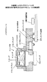
図1に示すカメラモジュール2は、大別して、レンズ部4と、モールド成型体6と、センサチップ8と、フレキシブル基板10とより構成される。レンズ部4は、2枚のレンズ4−1,4−2と、これを保持するレンズバレル4−3と、レンズバレル4−3を保持するレンズホルダ4−4とよりなる。レンズホルダ4−4はモールド成型体6に取り付けられる。モールド成型体6の内部には半導体素子としてプロセッサチップ12がモールドされている。モールド成型体の内部には、プロセッサチップ12の動作に関連した能動素子として図1に示す例ではチップコンデンサ14もモールドされている。 The camera module 2 shown in FIG. 1 is roughly composed of a lens unit 4, a molded body 6, a sensor chip 8, and a flexible substrate 10. The lens unit 4 includes two lenses 4-1 and 4-2, a lens barrel 4-3 that holds the lenses, and a lens holder 4-4 that holds the lens barrel 4-3. The lens holder 4-4 is attached to the molded body 6. Inside the molded body 6, a processor chip 12 is molded as a semiconductor element. In the example shown in FIG. 1, a chip capacitor 14 is also molded in the molded body as an active element related to the operation of the processor chip 12.
モールド成型体には貫通開口が形成されており、レンズ部4は開口を覆うようにモールド成型体6に取り付けられる。具体的にはレンズ部4のレンズホルダ4−4が接着剤によりモールド成型体6に固定される。一方、撮像素子としてのセンサチップ8の電極は、モールド成型体の貫通開口を介してレンズ部4のレンズ4−1,4−2に対向する位置に、受光面をレンズ4−2に向けた状態でモールド成型体6の底面に形成された端子に接続されている。したがって、レンズを通過した光は貫通開口を通過してセンサチップ8の受光面に入射し、受光面上に像が形成される。この像はセンサチップ8により電気信号に変換され、プロセッサチップ12により処理されて画像信号となり、フレキシブル基板10を介して外部の回路に出力される。 A through-opening is formed in the molded body, and the lens unit 4 is attached to the molded body 6 so as to cover the opening. Specifically, the lens holder 4-4 of the lens unit 4 is fixed to the molded body 6 with an adhesive. On the other hand, the electrode of the sensor chip 8 as the image pickup element has the light receiving surface directed to the lens 4-2 at a position facing the lenses 4-1 and 4-2 of the lens unit 4 through the through opening of the molded body. In the state, it is connected to a terminal formed on the bottom surface of the molded body 6. Therefore, the light that has passed through the lens passes through the through-opening and enters the light receiving surface of the sensor chip 8, and an image is formed on the light receiving surface. This image is converted into an electrical signal by the sensor chip 8, processed by the processor chip 12 to be an image signal, and output to an external circuit via the flexible substrate 10.
なお、レンズ4−2の下側には、ローパスフィルタ16が配置される。また、フレキシブル基板10は画像信号を外部に出力するための基板であるが、画像処理用の半導体チップや他の電子回路部品18を搭載することもできる。 A low-pass filter 16 is disposed below the lens 4-2. The flexible substrate 10 is a substrate for outputting image signals to the outside, but a semiconductor chip for image processing and other electronic circuit components 18 can also be mounted.
モールド成型体6は、いわゆるバンプチップキャリア(BCC)構造の半導体装置として機能する。すなわち、モールド成型体6の底面には樹脂突起が形成され、樹脂突起の表面に端子が形成されている。また、モールド成型体6の底面には配線パターンも形成されセンサチップ8、プロセッサチップ12、フレキシブル基板10は電気的に接続されている。 The molded body 6 functions as a semiconductor device having a so-called bump chip carrier (BCC) structure. That is, a resin protrusion is formed on the bottom surface of the molded body 6 and a terminal is formed on the surface of the resin protrusion. In addition, a wiring pattern is also formed on the bottom surface of the molded body 6, and the sensor chip 8, the processor chip 12, and the flexible substrate 10 are electrically connected.
以上のような構成のカメラモジュール2は、例えば携帯電話やポータブルコンピュータに内蔵され、周囲の映像を撮像して画像信号を得るためのカメラとして機能する。 The camera module 2 configured as described above is built in, for example, a mobile phone or a portable computer, and functions as a camera for capturing an image of surroundings and obtaining an image signal.
次に、本発明によるカメラモジュールの製造方法について説明する。本発明によるカメラモジュールの製造方法によれば、モールド成型体を複数個繋がった状態で形成し、その各々に対してセンサチップとレンズを搭載した後で、モールド成型体を個片化する。従来のカメラモジュールの製造方法のようにモールド成型体を形成した後直ちに個片化しないため、センサチップとレンズを複数のモールド成型体に対して一括して搭載することができる。 Next, a method for manufacturing a camera module according to the present invention will be described. According to the method for manufacturing a camera module of the present invention, a plurality of molded bodies are formed in a connected state, and after mounting a sensor chip and a lens on each of them, the molded bodies are separated into pieces. Since the molded body is not separated immediately after the molded body is formed as in the conventional method of manufacturing a camera module, the sensor chip and the lens can be collectively mounted on a plurality of molded bodies.
本発明によるカメラモジュールの製造工程では、まず、従来と同様に基板(リードフレーム)上に半導体チップであるプロセッサチップ12を搭載し、リードフレーム上でプロセッサチップ12をモールドしてモールド成型体6を形成する。リードフレームは複数のモールド成型体6が形成できるような大きさであり、モールド成型体6は樹脂で繋がった状態で複数個リードフレーム上に形成される。複数のモールド成型体6が形成された後リードフレームをエッチングして除去し、各モールド成型体6の貫通開口を有する底面を露出させる。なお、リードフレームを除去することにより各モールド成型体6の底面にはパターン配線及び端子が露出する。 In the manufacturing process of the camera module according to the present invention, first, the processor chip 12 which is a semiconductor chip is mounted on a substrate (lead frame) as in the prior art, and the processor chip 12 is molded on the lead frame to form the molded body 6. Form. The lead frame is sized so that a plurality of molded bodies 6 can be formed, and a plurality of molded bodies 6 are formed on the lead frame in a state of being connected by a resin. After the plurality of molded bodies 6 are formed, the lead frame is removed by etching, and the bottom surface having the through opening of each molded body 6 is exposed. In addition, pattern wiring and a terminal are exposed to the bottom face of each molded body 6 by removing the lead frame.
続いて、モールド成型体6が繋がって形成された樹脂成型体20上にセンサチップ8を搭載する。樹脂成型体20上に複数のセンサチップ8を一括して搭載する工程を図2に示す。図2において、樹脂成型体20は9×3=27個のモールド成型体6を一体的に形成したものであり、27個の貫通開口20aが形成されている。
Subsequently, the sensor chip 8 is mounted on the resin molded
上述のような樹脂成型体20に対して、27個のセンサチップ8を一括して搭載するために、搭載位置に合わせてセンサチップ8を整列して保持する。センサチップ8の保持は真空吸着装置22により行なう。真空吸着装置22で吸着・保持された27個のセンサチップ8は、モールド成型体6と同じ配列で配置されており、真空吸着ヘッド22全体を図2に示すように樹脂成型体20の上方に配置して、27個のセンサチップ8を一括して対応するモールド成型体6に搭載する。
In order to collectively mount the 27 sensor chips 8 on the resin molded
ここで、27個のセンサチップ8の位置は、対応するモールド成型体の所定の位置に合うように調整する必要がある。そこで、図3に示すように、真空吸着装置22の各センサチップを個別に吸着する吸着ヘッド22aに、XY方向に微小移動可能な駆動機構22bを設けている。図3は図2のIII−III線に沿った断面図である。図3に示すように、真空吸着装置22には、センサチップ8の各々を個別に吸着する吸着ヘッド22aが設けられ、各吸着ヘッド22aは駆動機構22bにより個別にXY方向に微小移動可能となっている。
Here, the positions of the 27 sensor chips 8 need to be adjusted so as to match the predetermined positions of the corresponding molded body. Therefore, as shown in FIG. 3, a drive mechanism 22 b that can be moved minutely in the XY directions is provided on the
センサチップ8を一括して樹脂成型体20に実装する際、樹脂成型体20における各モールド成型体6のセンサチップを実装する位置(あるいは位置を示すようなマーク)を画像認識し、画像認識による位置検出結果に基づいて駆動機構22bを駆動し、各吸着ヘッド22bのXY方向位置を個別に調整して位置補正を行う。樹脂成型体20は樹脂モールド品のためセンサチップ8を搭載する位置が僅かではあるがばらつくおそれがあり、またセンサチップ8を吸着ヘッド22aで吸着する際にも各センサチップ8の位置がばらつくおそれがある。このような要因によるセンサチップ8の取り付け位置のばらつきを補正するために吸着ヘッド22aに対して個別に駆動機構22bを設けている。
When the sensor chips 8 are collectively mounted on the resin molded
センサチップ8の取り付けが終了すると、次に、カメラモジュール2のレンズ部4となるレンズホルダ4−4を、樹脂成型体20に取り付ける。この際、27個のレンズホルダ4−4は、上述の真空吸着装置22又は同様な真空吸着装置を用いて一括に樹脂成型体20に取り付けられる。
When the attachment of the sensor chip 8 is completed, the lens holder 4-4 that becomes the lens unit 4 of the camera module 2 is then attached to the resin molded
以上の製造工程によれば、カメラモジュール2となるモールド成型体6が複数個繋がって形成された樹脂成型体20に対して、一括してセンサチップ8及びレンズホルダ4−4が取り付けられるので、複数個(この例では27個)のカメラモジュール2をまとめて処理することができ、製造工程を簡素化して効率的にカメラモジュールを製造することができる。
According to the above manufacturing process, the sensor chip 8 and the lens holder 4-4 are collectively attached to the resin molded
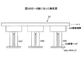
以上のように複数個一括して処理されて、センサチップ8及びレンズホルダ4−4が取り付けられた樹脂成型体20は、図4及び図5に示すように真空吸着テーブル24に吸着・固定され、ダイシングソーによりダイシングされて個片化される。真空吸着テーブル24は、図4に示すようにレンズホルダ4−4を収容する凹部又は孔24aと真空吸着用孔24bとを有する。図6は図5のVI−VI線に沿った断面図である。センサチップ8及びレンズホルダ4−4が取り付けられた樹脂成型体20のモールド成型体6に対応する部分の各々からはレンズホルダ4−4が突出しているので、レンズホルダ4−4が孔24aに収容された状態で真空吸着テーブル上に載置され、真空吸着用孔24bを介して吸着することにより、樹脂成型体20はセンサチップ8が上を向いた状態で真空吸着用孔24b上に固定される。
As described above, the resin molded
なお、レンズホルダ4−4の内部には、後からレンズ4−1,4−2及びローパスフィルタ16などの光学部品が組み込まれるため、レンズ4−4の内部を清浄に保つ必要がある。そこで、図6に示すように、真空吸着テーブル24の上面にシリコンゴムなどの防水シート26が設けられており、樹脂成型体20が真空吸着テーブル24に吸着された状態で樹脂成型体20と真空吸着テーブル24との間に挟まれてシールするようになっている。これにより、ダイシング時の冷却水やダイシングの切り屑が孔24aに進入しないようにシールされ、レンズホルダ4−4の内部に水や塵埃が入らないようになっている。
In addition, since the optical components such as the lenses 4-1 and 4-2 and the low-pass filter 16 are incorporated into the lens holder 4-4 later, it is necessary to keep the inside of the lens 4-4 clean. Therefore, as shown in FIG. 6, a waterproof sheet 26 made of silicon rubber or the like is provided on the upper surface of the vacuum suction table 24, and the resin molded
なお、本実施例では真空吸着テーブルを用いたが、これに限られず、樹脂成型体20を固定できるものであれば、例えば粘着テープによる貼り付けであってもかまわない。
In addition, although the vacuum suction table was used in the present Example, it is not restricted to this, For example, as long as the
樹脂成型体22を真空吸着用孔24b上に吸着・固定した後、ダイシングソーにより各モールド成型体6の繋がった部分を切り離すことにより、モールド成型体6に個片化される。次に、個片化された各モールド成型体6には、レンズ4−1,4−2及びローパスフィルタ16などの光学部品が組み込まれ、フレキシブル基板に搭載された後、試験が行われ、カメラモジュールとして完成する。
After the resin molded
以上のように、従来のカメラモジュールの製造方法では、1)リードフレームエッチング→2)PKGダイシング→3)PKGをフレキシブル基板に搭載→4)センサチップ搭載→5)洗浄→6)レンズホルダ搭載→7)試験、といった工程をとっていたが、本発明によるカメラモジュールの製造方法によれば、1)リードフレームエッチング→2)センサチップ搭載→3)洗浄→4)レンズ搭載→5)PKGダイシング→6)PKGをフレキシブル基板に搭載→7)試験といった順序となる。すなわち、従来の製造方法では、リードフレームを除去した直後にダイシングによりモールド成型体を個片化してしまい、その後は各モールド成型体について個別にセンサチップやレンズホルダを取り付けていたが、本発明によるカメラモジュールの製造方法によれば、リードフレームをエッチングにより除去した後、モールド成型体が繋がったままの状態でセンサチップ及びレンズホルダを取り付けるため、複数個のモールド成型体を一括して処理することができ、モールド成型体のハンドリングが簡単であり、効率的な製造工程となって生産性を向上することができる。 As described above, in the conventional camera module manufacturing method, 1) lead frame etching → 2) PKG dicing → 3) mounting PKG on flexible substrate → 4) mounting sensor chip → 5) cleaning → 6) mounting lens holder → 7) Tests were taken, but according to the camera module manufacturing method of the present invention, 1) lead frame etching → 2) sensor chip mounting → 3) cleaning → 4) lens mounting → 5) PKG dicing → 6) Mount PKG on flexible substrate → 7) Test order. That is, in the conventional manufacturing method, immediately after the lead frame is removed, the molded body is divided into pieces by dicing, and then the sensor chip and the lens holder are individually attached to each molded body. According to the manufacturing method of the camera module, after removing the lead frame by etching, in order to attach the sensor chip and the lens holder while the molded body is connected, a plurality of molded bodies are processed at once. Therefore, handling of the molded body is simple, and it becomes an efficient manufacturing process and productivity can be improved.
2 カメラモジュール
4 レンズ部
4−1,4−2 レンズ
4−3 レンズバレル
4−4 レンズホルダ
6 モールド成型体
8 センサチップ
10 フレキシブル基板
12 プロセッサチップ
14 チップコンデンサ
16 ローパスフィルタ
18 電子回路部品
20 樹脂成型体
22 真空吸着装置
22a 吸着ヘッド
22b 駆動機構
24 真空吸着テーブル
24a 穴
24b 真空吸着用孔
26 防水シート
2 Camera module 4 Lens part 4-1, 4-2 Lens 4-3 Lens barrel 4-4 Lens holder 6 Molded body 8 Sensor chip 10 Flexible substrate 12 Processor chip 14 Chip capacitor 16 Low pass filter 18
Claims (5)
前記モールド成型体が複数個繋がった状態で成型された樹脂成型体を準備し、
該樹脂成型体の前記モールド成型体に相当する部分の各々に対して前記カメラモジュールの構成部品を一括して取り付け、
該構成部品が取り付けられた状態で、前記樹脂成型体を切断して前記モールド成型体を個片化する
ことを特徴とするカメラモジュールの製造方法。 A method of manufacturing a camera module having a lens attached to a molded body, an imaging element, and a semiconductor element molded in the molded body,
Prepare a resin molded body molded in a state where a plurality of the molded bodies are connected,
The components of the camera module are collectively attached to each of the portions corresponding to the molded body of the resin molded body,
A method of manufacturing a camera module, comprising cutting the resin molded body and separating the molded body into pieces while the component parts are attached.
前記構成部品は、前記レンズを保持するためのレンズホルダ及び前記撮像素子の少なくとも一方であることを特徴とするカメラモジュールの製造方法。 A method of manufacturing a camera module according to claim 1,
The method of manufacturing a camera module, wherein the component is at least one of a lens holder for holding the lens and the imaging device.
前記構成部品を前記樹脂成型体に取り付ける際に、前記樹脂成型体における前記モールド成型体の配列と同じ配列で前記構成部品を真空吸着装置で保持しながら、前記構成部品を一括に前記樹脂成型体上に配置することを特徴とするカメラモジュールの製造方法。 It is a manufacturing method of the camera module according to claim 1 or 2,
When attaching the component parts to the resin molded body, holding the component parts in a vacuum adsorption device in the same arrangement as the mold molded body in the resin molded body, the component parts are collectively bundled with the resin molded body. A method of manufacturing a camera module, characterized by being arranged above.
前記構成部品を一括に前記樹脂成型体状に配置する際に、前記構成部品の各々を個別に微小移動して前記モールド成型体の配列に一致するように位置補正することを特徴とするカメラモジュールの製造方法。 A method of manufacturing a camera module according to claim 3,
A camera module characterized in that when the component parts are collectively arranged in the shape of the resin molded body, each of the component parts is finely moved individually to correct the position so as to match the arrangement of the molded bodies. Manufacturing method.
前記モールド成型体を個片化した後に、前記モールド部品を基板に搭載することを特徴とするカメラモジュールの製造方法。
A method for manufacturing a camera module according to any one of claims 1 to 4,
A method of manufacturing a camera module, wherein the molded component is separated into individual pieces, and then the molded component is mounted on a substrate.
Priority Applications (1)
| Application Number | Priority Date | Filing Date | Title |
|---|---|---|---|
| JP2004253111A JP2006074243A (en) | 2004-08-31 | 2004-08-31 | Method of manufacturing camera module |
Applications Claiming Priority (1)
| Application Number | Priority Date | Filing Date | Title |
|---|---|---|---|
| JP2004253111A JP2006074243A (en) | 2004-08-31 | 2004-08-31 | Method of manufacturing camera module |
Publications (1)
| Publication Number | Publication Date |
|---|---|
| JP2006074243A true JP2006074243A (en) | 2006-03-16 |
Family
ID=36154412
Family Applications (1)
| Application Number | Title | Priority Date | Filing Date |
|---|---|---|---|
| JP2004253111A Withdrawn JP2006074243A (en) | 2004-08-31 | 2004-08-31 | Method of manufacturing camera module |
Country Status (1)
| Country | Link |
|---|---|
| JP (1) | JP2006074243A (en) |
Cited By (4)
| Publication number | Priority date | Publication date | Assignee | Title |
|---|---|---|---|---|
| WO2007108414A1 (en) | 2006-03-17 | 2007-09-27 | Nikon Corporation | Exposure apparatus and device production method |
| KR100846623B1 (en) * | 2008-02-20 | 2008-07-16 | (주)네오스톰 | Cutting mold for camera module |
| CN101839800A (en) * | 2009-03-17 | 2010-09-22 | 鸿富锦精密工业(深圳)有限公司 | Lens fixing device |
| JP2018196103A (en) * | 2017-05-12 | 2018-12-06 | 海華科技股▲分▼有限公司 | Portable electronic apparatus, image photographing module, and placing unit |
-
2004
- 2004-08-31 JP JP2004253111A patent/JP2006074243A/en not_active Withdrawn
Cited By (5)
| Publication number | Priority date | Publication date | Assignee | Title |
|---|---|---|---|---|
| WO2007108414A1 (en) | 2006-03-17 | 2007-09-27 | Nikon Corporation | Exposure apparatus and device production method |
| KR100846623B1 (en) * | 2008-02-20 | 2008-07-16 | (주)네오스톰 | Cutting mold for camera module |
| CN101839800A (en) * | 2009-03-17 | 2010-09-22 | 鸿富锦精密工业(深圳)有限公司 | Lens fixing device |
| CN101839800B (en) * | 2009-03-17 | 2013-06-05 | 鸿富锦精密工业(深圳)有限公司 | Lens fixing device |
| JP2018196103A (en) * | 2017-05-12 | 2018-12-06 | 海華科技股▲分▼有限公司 | Portable electronic apparatus, image photographing module, and placing unit |
Similar Documents
| Publication | Publication Date | Title |
|---|---|---|
| US7796187B2 (en) | Wafer based camera module and method of manufacture | |
| US7539412B2 (en) | Camera module with first and second image sensor chips, holders and lens | |
| US7408205B2 (en) | Digital camera module | |
| US7964945B2 (en) | Glass cap molding package, manufacturing method thereof and camera module | |
| JP5814962B2 (en) | Small form factor module using flip-chip assembly with wafer level optics with cavity at bottom | |
| WO2007058073A1 (en) | Semiconductor package, method of producing the same, semiconductor module, and electronic apparatus | |
| CN109274876B (en) | Photosensitive assembly and packaging method thereof, lens module and electronic equipment | |
| KR20030091389A (en) | Image sensor module and construction method | |
| US20060223216A1 (en) | Sensor module structure and method for fabricating the same | |
| JP2014239446A (en) | Wafer level camera module and manufacturing method of the same | |
| JP2010525412A5 (en) | ||
| JP2008258949A (en) | Solid-state imaging apparatus | |
| KR20030022557A (en) | Module package of image capturing unit | |
| JP2007306387A (en) | Camera module and its manufacturing method | |
| JP4932745B2 (en) | Solid-state imaging device and electronic apparatus including the same | |
| JP2007282195A (en) | Camera lens module and manufacturing method therefor | |
| JP2004260155A (en) | Leadless lead frame electronic package and sensor module incorporating the same | |
| JP2006074243A (en) | Method of manufacturing camera module | |
| KR100756245B1 (en) | Camera module | |
| KR20020085120A (en) | Module package of image capturing unit | |
| KR100399640B1 (en) | Module package of image capturing unit | |
| JP4145619B2 (en) | OPTICAL MODULE AND ITS MANUFACTURING METHOD, CIRCUIT BOARD AND ELECTRONIC DEVICE | |
| JP4138436B2 (en) | Optical module, circuit board and electronic device | |
| KR20040001445A (en) | Housing of image sensor module | |
| KR20110123040A (en) | Image sensor package and camera module having the same |
Legal Events
| Date | Code | Title | Description |
|---|---|---|---|
| A300 | Application deemed to be withdrawn because no request for examination was validly filed |
Free format text: JAPANESE INTERMEDIATE CODE: A300 Effective date: 20071106 |