JP2006026401A - Detector for radiation imaging system - Google Patents
Detector for radiation imaging system Download PDFInfo
- Publication number
- JP2006026401A JP2006026401A JP2005184549A JP2005184549A JP2006026401A JP 2006026401 A JP2006026401 A JP 2006026401A JP 2005184549 A JP2005184549 A JP 2005184549A JP 2005184549 A JP2005184549 A JP 2005184549A JP 2006026401 A JP2006026401 A JP 2006026401A
- Authority
- JP
- Japan
- Prior art keywords
- sensor array
- electronic device
- interposer
- signal
- ray
- Prior art date
- Legal status (The legal status is an assumption and is not a legal conclusion. Google has not performed a legal analysis and makes no representation as to the accuracy of the status listed.)
- Granted
Links
- 238000003384 imaging method Methods 0.000 title claims abstract description 21
- 230000005855 radiation Effects 0.000 title claims description 18
- 230000008878 coupling Effects 0.000 claims abstract description 6
- 238000010168 coupling process Methods 0.000 claims abstract description 6
- 238000005859 coupling reaction Methods 0.000 claims abstract description 6
- 238000002591 computed tomography Methods 0.000 claims description 15
- 230000000875 corresponding effect Effects 0.000 description 20
- 108091006146 Channels Proteins 0.000 description 10
- 239000000463 material Substances 0.000 description 10
- XUIMIQQOPSSXEZ-UHFFFAOYSA-N Silicon Chemical compound [Si] XUIMIQQOPSSXEZ-UHFFFAOYSA-N 0.000 description 6
- 229910052710 silicon Inorganic materials 0.000 description 6
- 239000010703 silicon Substances 0.000 description 6
- 230000008901 benefit Effects 0.000 description 5
- 238000000034 method Methods 0.000 description 4
- 238000005070 sampling Methods 0.000 description 4
- 239000000758 substrate Substances 0.000 description 4
- 238000006243 chemical reaction Methods 0.000 description 3
- 230000002596 correlated effect Effects 0.000 description 3
- 238000001514 detection method Methods 0.000 description 3
- 238000010586 diagram Methods 0.000 description 3
- 239000010410 layer Substances 0.000 description 3
- 239000003990 capacitor Substances 0.000 description 2
- 230000005669 field effect Effects 0.000 description 2
- 229910052751 metal Inorganic materials 0.000 description 2
- 239000002184 metal Substances 0.000 description 2
- 238000012986 modification Methods 0.000 description 2
- 230000004048 modification Effects 0.000 description 2
- 230000003287 optical effect Effects 0.000 description 2
- 230000008569 process Effects 0.000 description 2
- 230000009467 reduction Effects 0.000 description 2
- 239000004065 semiconductor Substances 0.000 description 2
- MARUHZGHZWCEQU-UHFFFAOYSA-N 5-phenyl-2h-tetrazole Chemical compound C1=CC=CC=C1C1=NNN=N1 MARUHZGHZWCEQU-UHFFFAOYSA-N 0.000 description 1
- 102000001671 Acid Sensing Ion Channels Human genes 0.000 description 1
- 108010068806 Acid Sensing Ion Channels Proteins 0.000 description 1
- JBRZTFJDHDCESZ-UHFFFAOYSA-N AsGa Chemical compound [As]#[Ga] JBRZTFJDHDCESZ-UHFFFAOYSA-N 0.000 description 1
- 229910001218 Gallium arsenide Inorganic materials 0.000 description 1
- 238000009825 accumulation Methods 0.000 description 1
- 230000003321 amplification Effects 0.000 description 1
- 238000004458 analytical method Methods 0.000 description 1
- 238000003491 array Methods 0.000 description 1
- QWUZMTJBRUASOW-UHFFFAOYSA-N cadmium tellanylidenezinc Chemical compound [Zn].[Cd].[Te] QWUZMTJBRUASOW-UHFFFAOYSA-N 0.000 description 1
- 239000000919 ceramic Substances 0.000 description 1
- 239000013078 crystal Substances 0.000 description 1
- 238000009792 diffusion process Methods 0.000 description 1
- 230000000694 effects Effects 0.000 description 1
- 230000001939 inductive effect Effects 0.000 description 1
- 150000002739 metals Chemical class 0.000 description 1
- 238000003199 nucleic acid amplification method Methods 0.000 description 1
- 239000004033 plastic Substances 0.000 description 1
- 238000002600 positron emission tomography Methods 0.000 description 1
- HBMJWWWQQXIZIP-UHFFFAOYSA-N silicon carbide Chemical compound [Si+]#[C-] HBMJWWWQQXIZIP-UHFFFAOYSA-N 0.000 description 1
- 229910010271 silicon carbide Inorganic materials 0.000 description 1
- 239000002356 single layer Substances 0.000 description 1
- 230000003068 static effect Effects 0.000 description 1
- 238000002604 ultrasonography Methods 0.000 description 1
Images


Classifications
-
- G—PHYSICS
- G01—MEASURING; TESTING
- G01T—MEASUREMENT OF NUCLEAR OR X-RADIATION
- G01T1/00—Measuring X-radiation, gamma radiation, corpuscular radiation, or cosmic radiation
- G01T1/29—Measurement performed on radiation beams, e.g. position or section of the beam; Measurement of spatial distribution of radiation
- G01T1/2914—Measurement of spatial distribution of radiation
- G01T1/2921—Static instruments for imaging the distribution of radioactivity in one or two dimensions; Radio-isotope cameras
- G01T1/2928—Static instruments for imaging the distribution of radioactivity in one or two dimensions; Radio-isotope cameras using solid state detectors
-
- G—PHYSICS
- G01—MEASURING; TESTING
- G01T—MEASUREMENT OF NUCLEAR OR X-RADIATION
- G01T1/00—Measuring X-radiation, gamma radiation, corpuscular radiation, or cosmic radiation
- G01T1/16—Measuring radiation intensity
- G01T1/20—Measuring radiation intensity with scintillation detectors
- G01T1/2018—Scintillation-photodiode combinations
Landscapes
- Physics & Mathematics (AREA)
- Health & Medical Sciences (AREA)
- Life Sciences & Earth Sciences (AREA)
- General Physics & Mathematics (AREA)
- High Energy & Nuclear Physics (AREA)
- Molecular Biology (AREA)
- Spectroscopy & Molecular Physics (AREA)
- Measurement Of Radiation (AREA)
- Apparatus For Radiation Diagnosis (AREA)
- Light Receiving Elements (AREA)
Abstract
Description
本発明は、一般にイメージングシステムに関し、より具体的には放射線イメージングシステムの検出器システムに関する。 The present invention relates generally to imaging systems, and more particularly to detector systems for radiation imaging systems.
多くのイメージングシステムは、センサアレイと読み出し電子装置チャネルとの間の信号のフレキシブルルーティング及びスイッチングを必要とする可能性がある。このような要件の理由の幾つかには、より良好な電気的性能、読み出し電子回路のより大きなダイナミックレンジ、より良好な画像品質及びより大きな検出器面積が含まれる。ボリュームCTシステムなどの用途では、より大きな面積のアレイを備えた検出器を必要とする。 Many imaging systems may require flexible routing and switching of signals between the sensor array and the readout electronics channel. Some of the reasons for such requirements include better electrical performance, greater dynamic range of readout electronics, better image quality, and greater detector area. Applications such as volume CT systems require detectors with larger area arrays.
制限されたダイナミックレンジの読み出し電子回路は、電界効果トランジスタ(FET)スイッチを用いたピクセルの静的ビニングによって対処することができる。例えば、低い信号レベルを備えたCTスキャンでは、FETスイッチは、異なるピクセルからの信号を単一のASICチャネルに結合するように設定される。FETは通常、ベアのシリコンダイ上に形成され、X線センサに近接した位置にある検出器モジュール上に実装される。通常、FETのパッドは、例えばワイヤーボンディングでセンサピクセルアレイ及びASICボード上に電気的に接続される。多くの場合、センサコンタクトは、X線信号を受信する側面と同じ側面に形成されるため、X線検出に利用可能なアクティブ区域が縮小される結果となる。 Limited dynamic range readout electronics can be addressed by static binning of pixels using field effect transistor (FET) switches. For example, in a CT scan with a low signal level, the FET switch is set to combine signals from different pixels into a single ASIC channel. The FET is typically formed on a bare silicon die and mounted on a detector module located in close proximity to the x-ray sensor. Typically, the FET pads are electrically connected to the sensor pixel array and ASIC board, for example, by wire bonding. In many cases, the sensor contact is formed on the same side as the side receiving the X-ray signal, resulting in a reduction in the active area available for X-ray detection.
また、単一のチャネルを用いて複数の電気信号をピクセルから電子装置に動的にルーティングすることが要求される。所定時間内での単一チャネルへの複数のピクセル信号の動的ルーティングは、一般に高帯域FETを用いて達成され、該FETはリアルタイムで動作して、ビューの間に全ての適切なピクセルが指定チャネルを通じて読み出される。このような動的FETは通常、別々の構成要素としてパッケージされ、センサから離れたプリント基板上に実装される。加えて、FETの遠隔取り付けは、全てのピクセルに対する接続を基板にルーティングすることが必要となる。 There is also a requirement to dynamically route multiple electrical signals from the pixel to the electronic device using a single channel. Dynamic routing of multiple pixel signals to a single channel within a given time is typically accomplished using high-bandwidth FETs that operate in real time and all appropriate pixels are specified during the view. Read through the channel. Such dynamic FETs are typically packaged as separate components and mounted on a printed circuit board that is remote from the sensor. In addition, remote mounting of FETs requires routing connections for all pixels to the substrate.
信号を動的にルーティングする別の理由は、隣接したチャネルからの信号を異なる電子装置、通常は特定用途向け集積回路(ASIC)にルーティングするディザリング機能を提供することである。例えば、CTシステムにおけるディザリングの利点は、CTシステムの背景ノイズと組み合わせて見たときに、1つのASICの別のASICに対する線形性の差異が、再構成画像のチェッカーボードパターンを生成することである。通常、ディザリングは、プリント基板上に信号をルーティングすることによって達成される。プリント基板に関する1つの問題は、電気的に導通するトレース幅の寸法が大きいことであり、従って、ディザリングを達成するためには大きなボード面積及び幾つかの導通する層を必要とする。 Another reason for dynamically routing signals is to provide a dithering function that routes signals from adjacent channels to different electronic devices, typically application specific integrated circuits (ASICs). For example, the advantage of dithering in a CT system is that when viewed in combination with the CT system background noise, the difference in linearity of one ASIC to another ASIC generates a checkerboard pattern of reconstructed images. is there. Usually, dithering is accomplished by routing signals on the printed circuit board. One problem with printed circuit boards is the large size of the electrically conducting trace width, thus requiring a large board area and several conducting layers to achieve dithering.
検出器の別の望ましい特徴は、検出器面積が大きいことである。大きな面積を備えた検出器を設計する1つの問題は、検出器の電気的性能に影響を及ぼす電子ノイズが導入されることである。電子ノイズの可能性のある原因は、トレースルーティングの設計不良、すなわち、長いトレースの自己キャパシタンス、及び他の電子装置がトレースに近接して位置することが含まれる。加えて、トレースの間のキャパシタンスは、電子ノイズの原因となる可能性があるチャネル間のクロストークを招く。 Another desirable feature of the detector is a large detector area. One problem in designing detectors with large areas is that electronic noise is introduced that affects the electrical performance of the detector. Possible causes of electronic noise include poor trace routing design, ie, long trace self-capacitance, and other electronic devices located close to the trace. In addition, the capacitance between the traces causes crosstalk between channels that can cause electronic noise.
大きな検出器面積に望ましい別の特徴は、スイッチング回路をセンサアレイに近接して配置することであり、従って、センサアレイとスイッチング回路との間に最小のキャパシタンスが生じる。こうした物理的構成は、実質的にノイズ性能及び2つの重要な収集モード、すなわち相関二重サンプリング及び電荷蓄積収集シーケンスの効率を改善する。相関二重サンプリングは、ノイズを低減するためのアナログ電子工学の技術分野で公知の収集シーケンス手法であり、電荷蓄積は、単一の増幅チャネルに対して複数のピクセルを順序付ける手法である。通常、従来の検出器においては、スイッチング回路は、センサ自体からある距離の位置にあるボード又は基板上に実装されたディスクリート回路として存在する。センサとスイッチ回路との間のルーティングは、有意なキャパシタンス(約10から100ピコファラッド)をもたらし、2つの収集方式の効率を低減する。 Another feature desirable for large detector areas is the placement of the switching circuit in close proximity to the sensor array, thus resulting in minimal capacitance between the sensor array and the switching circuit. Such a physical configuration substantially improves noise performance and the efficiency of two important acquisition modes: correlated double sampling and charge storage collection sequences. Correlated double sampling is a collection sequence technique known in the analog electronics art for reducing noise, and charge accumulation is an ordering technique for multiple pixels for a single amplification channel. Usually, in conventional detectors, the switching circuit exists as a discrete circuit mounted on a board or substrate at a distance from the sensor itself. Routing between the sensor and the switch circuit results in significant capacitance (approximately 10 to 100 picofarads) and reduces the efficiency of the two collection schemes.
ほとんどの検出器システムに存在する別の問題は、1つの読み出し電子回路装置が別の装置とわずかに異なる比例関係で電荷をデジタル信号に変換するときに、ブロックアーチファクトが生成されることである。この差違は、電子装置のオフセット又はゲインにそれぞれ対応する低い信号値又は高い信号値で存在する可能性がある。 Another problem that exists in most detector systems is that block artifacts are created when one readout electronics device converts charge into a digital signal in a slightly different proportional relationship to another device. This difference may exist with low or high signal values corresponding respectively to the offset or gain of the electronic device.
加えて、センサ接続アレイのパターンは、電子装置の接続アレイと同じではない可能性がある。多くの場合、電子装置はセンサアレイよりも面積が小さく、そのコンタクトのピッチはより微細である。また、アレイパターンの違いはノイズをもたらす場合がある。加えて、ピクセルピッチの変化は一般に、センサと電子装置の間の多層フレックス回路をルーティングすることによって得られる。一般的にこうした回路のトレース長は長く、キャパシタンスの付加及び信号経路に対するノイズの誘因となる。
従って、大きな検出器面積と同時に、電気的性能、読み出し電子回路のダイナミックレンジを改善し、並びに良好な画像品質を提供する検出器設計に対する必要性がある。 Thus, there is a need for a detector design that improves electrical performance, readout electronics dynamic range, as well as large detector area, as well as providing good image quality.
要約すると、本発明の1つの態様によれば、イメージングシステムにおいて使用する検出器が提供される。該検出器は、X線信号を受信して該X線信号を対応する電気信号に変換するように構成された少なくとも1つのセンサアレイと、電子信号を対応するデジタル信号に変換するように構成された少なくとも1つの電子装置と、センサアレイと電子装置とを結合するスイッチング回路とを備え、該スイッチング回路は電気信号をセンサアレイから電子装置にルーティングするように構成される。 In summary, according to one aspect of the present invention, a detector for use in an imaging system is provided. The detector is configured to receive an X-ray signal and convert the X-ray signal to a corresponding electrical signal and to convert the electronic signal to a corresponding digital signal. At least one electronic device and a switching circuit coupling the sensor array and the electronic device, the switching circuit configured to route electrical signals from the sensor array to the electronic device.
別の実施形態においては、対象物の画像を生成するためのX線イメージングシステムが提供される。イメージングシステムは、対象物に対してX線放射線が対象物を透過するように構成された空間関係で配置されたX線源と、該X線放射線を対応する電気信号に変換するように構成された少なくとも1つの一体型検出器モジュールと、電気信号を処理して対象物の画像を生成するためのプロセッサとを備える。前記検出器は、X線信号を受信して該X線信号を対応する電気信号に変換するように構成された少なくとも1つのセンサアレイと、電気信号を対応するデジタル信号に変換するように構成された少なくとも1つの電子装置と、センサアレイと電子装置を結合し、電気信号をセンサアレイから電子装置にルーティングするために構成された少なくとも1つのスイッチング回路とから構成される。 In another embodiment, an x-ray imaging system for generating an image of an object is provided. The imaging system is configured to convert an X-ray radiation into a corresponding electrical signal and an X-ray source arranged in a spatial relationship configured to transmit the X-ray radiation to the object through the object. And at least one integrated detector module and a processor for processing the electrical signal to generate an image of the object. The detector is configured to receive an X-ray signal and convert the X-ray signal into a corresponding electrical signal and at least one sensor array configured to convert the electrical signal into a corresponding digital signal. And at least one electronic device and at least one switching circuit configured to couple the sensor array and the electronic device and route electrical signals from the sensor array to the electronic device.
別の実施形態においては、対象物の画像を生成するためのコンピュータ断層撮影(CT)システムが提供される。該CTシステムは、放射線のストリームを放出するよう構成されたX線源と、X線放射線を対応する電気信号に変換するように構成された少なくとも1つの一体化された検出器モジュールと、電気信号を処理して対象物の画像を生成するためのプロセッサを備える。前記検出器は、X線信号を受信して該X線信号を対応する電気信号に変換するように構成された少なくとも1つのセンサアレイと、電気信号を対応するデジタル信号に変換するように構成された少なくとも1つの電子装置と、センサアレイ及び電子装置を結合し、電気信号をセンサアレイから電子装置にルーティングするように構成された少なくとも1つのスイッチング回路から構成される。 In another embodiment, a computed tomography (CT) system for generating an image of an object is provided. The CT system includes an X-ray source configured to emit a stream of radiation, at least one integrated detector module configured to convert X-ray radiation into a corresponding electrical signal, and an electrical signal And a processor for generating an image of the object. The detector is configured to receive an X-ray signal and convert the X-ray signal into a corresponding electrical signal and at least one sensor array configured to convert the electrical signal into a corresponding digital signal. And at least one electronic circuit and at least one switching circuit configured to couple the sensor array and the electronic device and to route electrical signals from the sensor array to the electronic device.
別の実施形態において、一体化センサアレイキットが提供される。一体化されたセンサアレイキットは、X線信号を受信して該X線信号を対応する電気信号に変換するように構成された少なくとも1つのセンサアレイと、電子信号を対応するデジタル信号に変換するように構成された少なくとも1つの電子装置とを備える。前記センサアレイは更に、センサアレイと電子装置を結合し、電気信号をセンサアレイから電子装置にルーティングするように構成された少なくとも1つのスイッチング回路を備える。スイッチング回路は、第1の側面及び第2の側面を含むインターポーザー回路を含み、該インターポーザー回路がセンサアレイと電子装置との間に配置され且つ電子装置にセンサアレイを結合するように構成される。貫通ビアが、第1の側面と第2の側面とを電気的に結合するために備えられる。センサアレイキットは更に、インターポーザーの下に配置されたフレキシブルプリント回路を更に備え、電子装置は該フレキシブルプリント回路上に実装される。 In another embodiment, an integrated sensor array kit is provided. The integrated sensor array kit converts at least one sensor array configured to receive an x-ray signal and convert the x-ray signal into a corresponding electrical signal and an electronic signal into a corresponding digital signal. And at least one electronic device configured as described above. The sensor array further comprises at least one switching circuit configured to couple the sensor array and the electronic device and route electrical signals from the sensor array to the electronic device. The switching circuit includes an interposer circuit that includes a first side and a second side, the interposer circuit being disposed between the sensor array and the electronic device and configured to couple the sensor array to the electronic device. The A through via is provided to electrically couple the first side and the second side. The sensor array kit further includes a flexible printed circuit disposed under the interposer, and the electronic device is mounted on the flexible printed circuit.
本発明のこれら及び他の特徴、態様、及び利点は、図面全体を通して同じ符号が同じ部分を示す添付図面を参考しながら以下の詳細な説明を読むとより理解されるであろう。 These and other features, aspects and advantages of the present invention will become better understood when the following detailed description is read with reference to the accompanying drawings in which like numerals indicate like parts throughout the drawings.
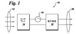
図1は、X線イメージングシステムでの使用に適合された検出器モジュールのブロック図である。X線イメージングシステムの例には、コンピュータ・トモシンセンスシステム、陽電子放射断層撮影法システムなどが含まれる。検出器モジュール10は、センサアレイ14、スイッチング回路16及び電子装置19を含む一体化構造体である。各構成要素は更に詳細に以下に説明される。
FIG. 1 is a block diagram of a detector module adapted for use in an X-ray imaging system. Examples of X-ray imaging systems include computer tomosynthesis systems, positron emission tomography systems, and the like. The
ここで用いられる「適合された」、「構成された」及び同様の用語は、システム内の装置が、システムの各要素が協働して説明される効果を提供することができるようにされていることを意味し、これらの用語はまた、アナログ又はデジタルのコンピュータ又は特定用途デバイス(特定用途向け集積回路(ASIC)など)の電気的又は光学的要素の動作機能、所与の入力信号に応答して出力を供給するようにプログラムされた増幅器又は同様のもの、及び電気的又は光学的に部品を互いに結合するための機械的装置を意味する。 As used herein, “adapted”, “configured” and like terms are intended to allow devices within the system to provide the effect that each element of the system cooperates with. These terms also mean the operational function of electrical or optical elements of an analog or digital computer or application-specific device (such as application-specific integrated circuit (ASIC)), responsive to a given input signal An amplifier or the like programmed to provide an output and a mechanical device for electrically or optically coupling components together.
センサアレイ14は、X線信号を受信し、及びX線信号を対応する電気信号に変換するよう構成される。センサアレイ16は、複数のピクセル22を含み、フォトダイオードを備えたシンチレータ及び直接変換材料などのX線検出材料を含む。例示的な実施形態において、センサアレイは、例えば、X線放射線を対応する電気信号に変換するよう構成されたX線検出媒体を含むことができる。
The
電子装置18は、電気信号を対応するデジタル信号20に変換するように構成される。電子装置18は、図1には示していない、増幅器、コンデンサ、サンプリング回路などを含むことができる。デジタル信号は、デジタル信号を処理して対応する画像を生成することができる画像プロセッサに供給することができる。
The
スイッチング回路16は、センサアレイ14と電子装置18を結合するように構成される。スイッチング回路は、センサアレイのピクセルから電気信号を電子装置に経路に沿ってルーティングするように構成される。1つの実施形態においては、スイッチング回路は、インターポーザー回路を含む。センサアレイの直下にスイッチング回路を配置することにより、センサアレイとスイッチング回路との間のキャパシタンスが実質的に低減され、従って、全体のノイズの低減を含む電気的性能が改善される。加えて、センサアレイの近傍にスイッチング回路を配置することによって、電子装置のチャネルの相関二重サンプリングが行われ、従って、更に、インターコネクショントレースのノイズが低減される。信号は検出器モジュール内でルーティングされるので、検出器モジュールの側面には突合せ機能が設けられる。従って、こうした幾つかの検出器モジュールを検出器モジュール10に付加して、2次元アレイを形成すると、大面積検出器アレイを生成することができる。
The switching
図2は、X線信号12を感知して、対応するデジタル信号20を生成するのに使用される検出器10の側面図である。図示の実施形態においては、複数のピクセル22から構成されるセンサアレイが示されている。センサアレイは、シリチレータ材料及びフォトダイオードを含むことができる。別の実施形態においては、センサアレイは、直接変換材料の単一の層から構成される。直接変換材料の例には、テルル化カドミウム、テルル化カドミウム亜鉛結晶、多結晶成形体及びフィルム層が含まれる。図示の実施形態においては、スイッチング回路16は、シリコンインターポーザー回路である。シリコンインターポーザー回路は、電子装置18に結合される。シリコンインターポーザー回路は、図3、図4及び図5を参照して以下に更に詳細に説明される。
FIG. 2 is a side view of the
図3は、インターポーザー回路の実施例の平面図である。インターポーザーは典型的には、トレースルーティング能力が最も高いシリコン基材を用いて作られる。しかしながら、当業者であれば、インターポーザーの基材材料は、シリコン、炭化ケイ素、ヒ素ガリウムなどを含む任意の半導体材料をから構成することができる点は理解されるであろう。加えて、有機及び非有機ポリマー材料は、インターポーザーの機能的要件に適合するように、トレースルーティング及び貫通ビアを備えて構成することができる。半導体材料を用いてインターポーザーを作る利点は、標準的なウェーハプロセスを用いてインターポーザーを作ることが可能であることであり、これにはウェーハ処理により達成できる極めて微細なピッチでインターポーザーの上に入力/出力コンタクトを生成することを含む。更に、インターポーザー材料は、その特性に基づき最適な機械的及び熱的性能に対応するように選択することができる。 FIG. 3 is a plan view of an embodiment of an interposer circuit. Interposers are typically made using a silicon substrate with the highest trace routing capability. However, those skilled in the art will appreciate that the interposer substrate material may be composed of any semiconductor material including silicon, silicon carbide, gallium arsenide, and the like. In addition, organic and non-organic polymeric materials can be configured with trace routing and through vias to meet the functional requirements of the interposer. The advantage of creating an interposer using semiconductor materials is that the interposer can be made using standard wafer processes, including an extremely fine pitch that can be achieved by wafer processing. Generating input / output contacts. Furthermore, the interposer material can be selected based on its properties to accommodate optimal mechanical and thermal performance.
第1の側面26を含むインターポーザー回路が示されている。第1の側面26は、幾つかのコンタクトパッド28を含む。1つの実施形態において、インターポーザーの第1の側面は、センサアレイの各ピクセルにつき1つのコンタクトパッドを含む。各コンタクトパッドは、センサアレイのピクセルコンタクトに対応するよう配置することができる。コンタクトパッドは、センサアレイ14とインターポーザー回路の第1の側面とを結合するよう構成される。
An interposer circuit including a
図4は、インターポーザー回路の1つの実施形態の底面図である。インターポーザー回路は、電子装置にインターポーザーを結合するよう構成された第2の側面30を含む。第2の側面は、電気的スイッチ34,36及び38に結合されたコンタクトパッド32を含む。電気的スイッチは、センサアレイからの電気信号を電子装置の所望のチャネルに多重送信するよう構成される。本発明の特定の実施形態において、種々のピクセルからの電気信号は、電子装置の単一チャネルを通じてルーティングすることができる。
FIG. 4 is a bottom view of one embodiment of an interposer circuit. The interposer circuit includes a
電気的スイッチの例としては、電界効果トランジスタ、スイッチとして構成されたダイオード、コンデンサスイッチ、及び類似するものが含まれる。インターポーザー回路の1つの特定の実施形態においては、電気的スイッチは、センサアレイ14(図1に示す)から電子装置18(図1に示す)までトレースを結合することができる。第2の側面は更に、スイッチのゲートラインを電子装置のコントロールシステムの制御ラインに結合する制御ライン(図示せず)を含むことができる。 Examples of electrical switches include field effect transistors, diodes configured as switches, capacitor switches, and the like. In one particular embodiment of the interposer circuit, an electrical switch can couple traces from the sensor array 14 (shown in FIG. 1) to the electronic device 18 (shown in FIG. 1). The second aspect can further include a control line (not shown) that couples the gate line of the switch to the control line of the control system of the electronic device.
図5は、インターポーザー回路16の1つの実施形態の断面図である。貫通ビア40は、第1の側面26と第2の側面30とを電気的に結合するよう構成される。貫通ビアは、規則的なアレイとすることができ、又はインターポーザー回路の1つの区域にクラスター化することができる。
FIG. 5 is a cross-sectional view of one embodiment of the
別の実施形態においては、図1の検出器は、図6に示されるようにフレキシブルプリント回路を更に含む。また、フレキシブルインターコネクションは、フレキシブルプリント回路の代わりに用いることができる。フレキシブルプリント回路は、図6に示されるようにインターポーザー回路の下に配置することができる。電子装置18は、フレキシブルプリント回路42上に配置される。電子装置は、プリント回路の任意の部分に配置することができ、従って、検出器10上に機械的支持体などの非電気的装置を用意に付加することが可能になる。バックプレーン44とは、セラミック、プラスチック、金属又は金属の組み合わせの支持構造を含むことができるスイッチング回路の機械的支持体を意味する。一般的に、バックプレーンは、機械的及び熱的機能の両方の役割を果たす。
In another embodiment, the detector of FIG. 1 further includes a flexible printed circuit as shown in FIG. The flexible interconnection can be used in place of the flexible printed circuit. The flexible printed circuit can be placed under the interposer circuit as shown in FIG. The
図7、図8及び図9は、スイッチング回路16及びフレキシブルプリント回路42を備える検出器の種々の実施形態である。図7は、フレキシブルプリント回路がスイッチング回路16の下に「T」字形に配置された1つの実施形態である。バックプレーン44は、スイッチング回路16の機械的支持体として適用される。クランプ46は、読み出し回路18の機械支持体である。熱拡散層48は、電子装置が発生した熱を放散するために電子装置18の下に配置される。
7, 8 and 9 are various embodiments of detectors comprising the switching
同様に、図8は、フレキシブルプリント回路がスイッチング回路16の下に「C」字形に配置された1つの実施形態であり、図9は、フレキシブルプリント回路がスイッチ回路16の下に「U」字形に配置された1つの実施形態である。センサから電子装置までのフレキシブルインターコネクションの他の形状及び構成は、詳細には示さないが可能である。
Similarly, FIG. 8 is one embodiment in which the flexible printed circuit is arranged in a “C” shape under the switching
上述の一体化された検出器モジュール10の実施形態は、CTシステムなどの種々の放射線イメージングシステムで実施することができる。体積に関する画像情報を収集する他のイメージング診断装置もまた、説明される本発明からの恩恵を受けることができる。CTシステムの以下の検討は、このような実施の単に例証に過ぎず、診断装置及び解剖学的分析の点で限定を意図するものではない。本発明はまた、超音波システム、光学システム、熱システムといった、1つの形態の信号を感知してこれを別の信号に変換する他のシステムに利用することができる。
Embodiments of the
図10は、イメージング対象64の一部のイメージングに使用された例示的なCTスキャンシステム50である。CTスキャンシステム50は、フレーム52及びアパーチャ56を有するガントリ54と共に図示されている。更に、テーブル58は、フレーム52及びガントリ54のアパーチャ56内に位置付けられて示されている。ガントリ54は、X線源12(典型的にはX線放射線を放出するX線管62)により示されている。通常運転においては、X線源62は、検出器モジュール10に向かってX線ビームを投影する。
FIG. 10 is an exemplary
検出器モジュール10は、図1及び図2を参照して説明されたセンサアレイ、スイッチング回路、及び電子装置から構成される一体化構造体である。検出器モジュールは、X線信号を受信し、該X線信号を対応する電気信号に変換するように構成された少なくとも1つのセンサアレイと、電子信号を対応するデジタル信号に変換するように構成された少なくとも1つの電子装置と、センサアレイ及び電子装置を結合するスイッチング回路とを含み、該スイッチング回路は電気信号をセンサアレイから電子装置にルーティングするよう構成されており、該スイッチング回路、センサアレイ、及び電子装置は一体化構造体を形成する。
The
検出器モジュール10からのデータは、プロセッサ66によりフィルタ処理及び逆投影されて、スキャンされた区域の画像を構築する。プロセッサ66は、通常、CTシステム10全体を制御するのに使用される。システムの動作を制御するメインプロセッサは、システムコントローラーによりイネーブルにされる機能を制御するよう適合させることができる。更に、オペレーターワークステーション70は、プロセッサ66並びにディスプレイ72に結合され、再構成された画像を見ることができるようになる。あるいは、本明細書で説明された処理の一部又は全ては、原画像又は部分的に処理された画像データに基づいて、追加のコンピュータ資源によって遠隔的に実施することができる。
Data from
上記で説明された本発明は、センサアレイと電子装置との間の信号のフレキシブルルーティングを可能にすることを含む、多くの利点を提供する。多重化、ビニングなどの種々の機能を提供するための全ての回路は、単一のチップで構築することができ、従って、システムをよりコンパクトで信頼性のあるものとする。 The invention described above provides a number of advantages, including enabling flexible routing of signals between the sensor array and the electronic device. All circuits for providing various functions such as multiplexing and binning can be built on a single chip, thus making the system more compact and reliable.
本発明の特定の特徴のみを本明細書で図示し説明してきたが、当業者であれば多くの修正及び変更が行われるであろう。従って、添付の請求項は、本発明の真の精神の範囲内にあるこのような修正及び変更を保護することを意図するものであることは理解されるべきである。また、図面の符号に対応する特許請求の範囲中の符号は、単に本願発明の理解をより容易にするために用いられているものであり、本願発明の範囲を狭める意図で用いられたものではない。そして、本願の特許請求の範囲に記載した事項は、明細書に組み込まれ、明細書の記載事項の一部となる。 While only certain features of the invention have been illustrated and described herein, many modifications and changes will occur to those skilled in the art. Accordingly, it is to be understood that the appended claims are intended to cover such modifications and changes as fall within the true spirit of the invention. Further, the reference numerals in the claims corresponding to the reference numerals in the drawings are merely used for easier understanding of the present invention, and are not intended to narrow the scope of the present invention. Absent. The matters described in the claims of the present application are incorporated into the specification and become a part of the description items of the specification.
10 検出器モジュール
12 X線信号
14 センサアレイ
16 スイッチング回路
18 電子装置
DESCRIPTION OF
Claims (10)
X線信号(12)を受信し、該X線信号を対応する電気信号に変換するように構成された少なくとも1つのセンサアレイ(14)と、
前記電子信号を対応するデジタル信号(20)に変換するように構成された少なくとも1つの電子装置(18)と、
前記センサアレイと前記電子装置とを結合するスイッチング回路(16)と、
を備え、
前記スイッチング回路が、前記電気信号を前記センサアレイから前記電子装置にルーティングするように構成され、前記スイッチング回路、前記センサアレイ、及び前記電子装置が一体化された構造体を形成することを特徴とする検出器モジュール。 A detector module (10) for use in an imaging system (50) comprising:
At least one sensor array (14) configured to receive an x-ray signal (12) and convert the x-ray signal into a corresponding electrical signal;
At least one electronic device (18) configured to convert the electronic signal into a corresponding digital signal (20);
A switching circuit (16) for coupling the sensor array and the electronic device;
With
The switching circuit is configured to route the electrical signal from the sensor array to the electronic device, and forms a structure in which the switching circuit, the sensor array, and the electronic device are integrated. Detector module.
前記対象物に対してX線放射線が該対象物を透過するように構成された空間関係で配置されたX線源と、
前記X線放射線を対応する電気信号に変換するように構成された少なくとも1つの一体化検出器モジュールと、
を備え、
前記一体化された検出器モジュールが、
X線信号を受信し、該X線信号を対応する電気信号に変換するように構成された少なくとも1つのセンサアレイと、
前記電気信号を対応するデジタル信号に変換するように構成された少なくとも1つの電子装置と、
前記センサアレイと前記電子装置とを結合し、前記電気信号を前記センサアレイから前記電子装置にルーティングするように構成された少なくとも1つのスイッチング回路と、
から構成され、前記システムが更に、
前記電気信号を処理して前記対象物の画像を生成するためのプロセッサを備えることを特徴とする放射線イメージングシステム。 An X-ray imaging system for generating an image of an object,
An X-ray source arranged in a spatial relationship configured to transmit X-ray radiation to the object through the object;
At least one integrated detector module configured to convert the x-ray radiation into a corresponding electrical signal;
With
The integrated detector module is
At least one sensor array configured to receive an x-ray signal and convert the x-ray signal into a corresponding electrical signal;
At least one electronic device configured to convert the electrical signal into a corresponding digital signal;
At least one switching circuit configured to couple the sensor array and the electronic device and route the electrical signal from the sensor array to the electronic device;
The system further comprising:
A radiation imaging system comprising a processor for processing the electrical signal to generate an image of the object.
放射線のストリームを放出するよう構成されたX線源(62)と、
前記X線放射線を対応する電気信号に変換するように構成された少なくとも1つの一体化された検出器モジュール(10)と、
を備え、
前記検出器が、
X線信号を受信して該X線信号を対応する電気信号に変換するように構成された少なくとも1つのセンサアレイ(14)と、
前記電子信号を対応するデジタル信号(20)に変換するように構成された少なくとも1つの電子装置(18)と、
前記センサアレイ及び前記電子装置を結合し、前記電気信号を前記センサアレイから前記電子装置にルーティングするように構成された少なくとも1つのスイッチング回路(16)であって、該スイッチング回路が、第1の側面(26)及び第2の側面(30)を含むインターポーザー回路を含み、前記インターポーザー回路が前記センサアレイと前記電子装置との間に配置され且つ前記センサアレイを前記電子装置に結合するように構成されている前記スイッチング回路と、
から構成され、前記システムが更に、
前記電気信号を処理して前記対象物の画像を生成するためのプロセッサ(66)を備えることを特徴とするコンピュータ断層撮影システム。 A computed tomography (CT) system for generating an image of an object comprising:
An X-ray source (62) configured to emit a stream of radiation;
At least one integrated detector module (10) configured to convert the x-ray radiation into a corresponding electrical signal;
With
The detector is
At least one sensor array (14) configured to receive an X-ray signal and convert the X-ray signal into a corresponding electrical signal;
At least one electronic device (18) configured to convert the electronic signal into a corresponding digital signal (20);
At least one switching circuit (16) configured to couple the sensor array and the electronic device and route the electrical signal from the sensor array to the electronic device, the switching circuit comprising: An interposer circuit including a side surface (26) and a second side surface (30), wherein the interposer circuit is disposed between the sensor array and the electronic device and couples the sensor array to the electronic device. The switching circuit configured to:
The system further comprising:
A computed tomography system comprising a processor (66) for processing the electrical signal to generate an image of the object.
X線信号(12)を受信して、該X線信号を対応する電気信号に変換するように構成された少なくとも1つのセンサアレイ(14)と、
前記電子信号を対応するデジタル信号(20)に変換するように構成された少なくとも1つの電子装置(18)と、
前記センサアレイ及び前記電子装置を結合し、前記電気信号を前記センサアレイから前記電子装置にルーティングするように構成された少なくとも1つのスイッチング回路(16)であって、前記スイッチング回路が、第1の側面(26)及び第2の側面(30)を含むインターポーザー回路を含み、該インターポーザー回路が前記センサアレイと前記電子装置との間に配置され且つ前記電子装置に前記センサアレイを結合するように構成されているスイッチング回路と、
前記第1の側面及び前記第2の側面を電気的に結合するように構成された貫通ビア(40)と、
前記インターポーザーの下に配置されたフレキシブルプリント回路(42)又はフレキシブルインターコネクションと、
を備え、
前記電子装置が前記フレキシブルプリント回路上に実装されることを特徴とする器から成ることを特徴とする一体化センサアレイキット。 An integrated sensor array kit,
At least one sensor array (14) configured to receive an X-ray signal (12) and convert the X-ray signal into a corresponding electrical signal;
At least one electronic device (18) configured to convert the electronic signal into a corresponding digital signal (20);
At least one switching circuit (16) configured to couple the sensor array and the electronic device and route the electrical signal from the sensor array to the electronic device, the switching circuit comprising: An interposer circuit including a side surface (26) and a second side surface (30), wherein the interposer circuit is disposed between the sensor array and the electronic device and couples the sensor array to the electronic device. A switching circuit configured in
A through via (40) configured to electrically couple the first side and the second side;
A flexible printed circuit (42) or a flexible interconnection disposed under the interposer;
With
An integrated sensor array kit comprising: a device characterized in that the electronic device is mounted on the flexible printed circuit.
Applications Claiming Priority (2)
| Application Number | Priority Date | Filing Date | Title |
|---|---|---|---|
| US10/881,950 US20050286682A1 (en) | 2004-06-29 | 2004-06-29 | Detector for radiation imaging systems |
| US10/881,950 | 2004-06-29 |
Publications (2)
| Publication Number | Publication Date |
|---|---|
| JP2006026401A true JP2006026401A (en) | 2006-02-02 |
| JP4949646B2 JP4949646B2 (en) | 2012-06-13 |
Family
ID=35505741
Family Applications (1)
| Application Number | Title | Priority Date | Filing Date |
|---|---|---|---|
| JP2005184549A Expired - Fee Related JP4949646B2 (en) | 2004-06-29 | 2005-06-24 | Radiation imaging system detector |
Country Status (4)
| Country | Link |
|---|---|
| US (1) | US20050286682A1 (en) |
| JP (1) | JP4949646B2 (en) |
| CN (1) | CN1717146A (en) |
| NL (1) | NL1029344C2 (en) |
Cited By (7)
| Publication number | Priority date | Publication date | Assignee | Title |
|---|---|---|---|---|
| JP2009078143A (en) * | 2007-09-26 | 2009-04-16 | General Electric Co <Ge> | Method and apparatus for flexibly binning energy discriminating data |
| JP2011226902A (en) * | 2010-04-20 | 2011-11-10 | Nec Tohoku Ltd | X-ray data acquisition device |
| JP2012143564A (en) * | 2011-01-13 | 2012-08-02 | General Electric Co <Ge> | Multi-slice ct detector with tileable packaging structure |
| JP2013106997A (en) * | 2013-03-12 | 2013-06-06 | Toshiba Corp | X-ray detecter system and x-ray ct apparatus |
| JP2014035293A (en) * | 2012-08-09 | 2014-02-24 | Hitachi Medical Corp | Radiation detector and x-ray ct device |
| JP2015114325A (en) * | 2013-12-09 | 2015-06-22 | オックスフォード インストゥルメンツ アナリティカル オーワイOxford Instruments Analytical Oy | Semiconductor radiation detector having large active area and method for manufacturing the same |
| JP2019523402A (en) * | 2016-07-14 | 2019-08-22 | コーニンクレッカ フィリップス エヌ ヴェKoninklijke Philips N.V. | DETECTOR MODULE, DETECTOR, IMAGING DEVICE AND DETECTOR MODULE MANUFACTURING METHOD |
Families Citing this family (11)
| Publication number | Priority date | Publication date | Assignee | Title |
|---|---|---|---|---|
| US7606346B2 (en) * | 2007-01-04 | 2009-10-20 | General Electric Company | CT detector module construction |
| CN101655465B (en) * | 2009-08-28 | 2012-03-07 | 北京睿思厚德辐射信息科技开发有限公司 | Dotted line composite scanning backscattered and stereo transmission imaging device |
| US9513384B2 (en) | 2011-11-08 | 2016-12-06 | Koninklijke Philips N.V. | Seamless tiling to build a large detector |
| US9689996B2 (en) * | 2013-04-05 | 2017-06-27 | General Electric Company | Integrated diode DAS detector |
| US9151851B2 (en) | 2013-06-27 | 2015-10-06 | General Electric Company | Mulitplexing device for a medical imaging system |
| US9960203B2 (en) | 2014-12-21 | 2018-05-01 | Ion Beam Applications S.A. | Radiation sensor |
| CN106405621B (en) * | 2016-08-31 | 2019-01-29 | 兰州大学 | A kind of focal spot size measurement method |
| DE102018219577A1 (en) * | 2018-11-15 | 2020-05-20 | Siemens Healthcare Gmbh | X-ray detector having a stack arrangement |
| CN110090038A (en) * | 2019-05-06 | 2019-08-06 | 明峰医疗系统股份有限公司 | A kind of CT spherical surface panel detector structure |
| CN113433584B (en) * | 2021-06-28 | 2022-11-04 | 哈尔滨工业大学 | Pixel circuit in pixel detector compatible with electron collection and hole collection |
| WO2024138731A1 (en) * | 2022-12-30 | 2024-07-04 | Shanghai United Imaging Healthcare Co., Ltd. | Systems, methods, and devices for imaging |
Citations (7)
| Publication number | Priority date | Publication date | Assignee | Title |
|---|---|---|---|---|
| JP2001215281A (en) * | 2000-02-02 | 2001-08-10 | Toshiba Corp | Two-dimensional detector for x-ray ct |
| JP2001318155A (en) * | 2000-02-28 | 2001-11-16 | Toshiba Corp | Radiation detector and x-ray ct device |
| JP2002034968A (en) * | 2000-07-25 | 2002-02-05 | Toshiba Corp | X-ray ct apparatus |
| JP2003066149A (en) * | 2000-08-14 | 2003-03-05 | Toshiba Corp | Radiation detector, radiation detecting system, x-ray ct system |
| JP2003098261A (en) * | 2001-09-25 | 2003-04-03 | Hitachi Medical Corp | X-ray ct apparatus |
| JP2003121551A (en) * | 2001-10-09 | 2003-04-23 | Toshiba Corp | Radiation detector and method of manufacturing the same, and x-ray ct equipment |
| JP2004008406A (en) * | 2002-06-05 | 2004-01-15 | Toshiba Corp | Method for manufacturing radiation detector, radiation detector, and x-ray ct apparatus |
Family Cites Families (7)
| Publication number | Priority date | Publication date | Assignee | Title |
|---|---|---|---|---|
| US4504962A (en) * | 1978-12-22 | 1985-03-12 | Emi Limited | Computerized tomography |
| US6259098B1 (en) * | 1999-05-17 | 2001-07-10 | General Electric Company | Low cost, low resolution interconnect for a solid-state x-ray detector |
| US6658082B2 (en) * | 2000-08-14 | 2003-12-02 | Kabushiki Kaisha Toshiba | Radiation detector, radiation detecting system and X-ray CT apparatus |
| JP2002125228A (en) * | 2000-10-17 | 2002-04-26 | Hitachi Ltd | System and method for expanding digital data |
| US6567495B2 (en) * | 2001-03-06 | 2003-05-20 | General Electric Company | Detector having programmable slice thickness and operational modes and method |
| US6510195B1 (en) * | 2001-07-18 | 2003-01-21 | Koninklijke Philips Electronics, N.V. | Solid state x-radiation detector modules and mosaics thereof, and an imaging method and apparatus employing the same |
| US7189971B2 (en) * | 2002-02-15 | 2007-03-13 | Oy Ajat Ltd | Radiation imaging device and system |
-
2004
- 2004-06-29 US US10/881,950 patent/US20050286682A1/en not_active Abandoned
-
2005
- 2005-06-24 JP JP2005184549A patent/JP4949646B2/en not_active Expired - Fee Related
- 2005-06-27 NL NL1029344A patent/NL1029344C2/en not_active IP Right Cessation
- 2005-06-29 CN CNA2005100818529A patent/CN1717146A/en active Pending
Patent Citations (7)
| Publication number | Priority date | Publication date | Assignee | Title |
|---|---|---|---|---|
| JP2001215281A (en) * | 2000-02-02 | 2001-08-10 | Toshiba Corp | Two-dimensional detector for x-ray ct |
| JP2001318155A (en) * | 2000-02-28 | 2001-11-16 | Toshiba Corp | Radiation detector and x-ray ct device |
| JP2002034968A (en) * | 2000-07-25 | 2002-02-05 | Toshiba Corp | X-ray ct apparatus |
| JP2003066149A (en) * | 2000-08-14 | 2003-03-05 | Toshiba Corp | Radiation detector, radiation detecting system, x-ray ct system |
| JP2003098261A (en) * | 2001-09-25 | 2003-04-03 | Hitachi Medical Corp | X-ray ct apparatus |
| JP2003121551A (en) * | 2001-10-09 | 2003-04-23 | Toshiba Corp | Radiation detector and method of manufacturing the same, and x-ray ct equipment |
| JP2004008406A (en) * | 2002-06-05 | 2004-01-15 | Toshiba Corp | Method for manufacturing radiation detector, radiation detector, and x-ray ct apparatus |
Cited By (7)
| Publication number | Priority date | Publication date | Assignee | Title |
|---|---|---|---|---|
| JP2009078143A (en) * | 2007-09-26 | 2009-04-16 | General Electric Co <Ge> | Method and apparatus for flexibly binning energy discriminating data |
| JP2011226902A (en) * | 2010-04-20 | 2011-11-10 | Nec Tohoku Ltd | X-ray data acquisition device |
| JP2012143564A (en) * | 2011-01-13 | 2012-08-02 | General Electric Co <Ge> | Multi-slice ct detector with tileable packaging structure |
| JP2014035293A (en) * | 2012-08-09 | 2014-02-24 | Hitachi Medical Corp | Radiation detector and x-ray ct device |
| JP2013106997A (en) * | 2013-03-12 | 2013-06-06 | Toshiba Corp | X-ray detecter system and x-ray ct apparatus |
| JP2015114325A (en) * | 2013-12-09 | 2015-06-22 | オックスフォード インストゥルメンツ アナリティカル オーワイOxford Instruments Analytical Oy | Semiconductor radiation detector having large active area and method for manufacturing the same |
| JP2019523402A (en) * | 2016-07-14 | 2019-08-22 | コーニンクレッカ フィリップス エヌ ヴェKoninklijke Philips N.V. | DETECTOR MODULE, DETECTOR, IMAGING DEVICE AND DETECTOR MODULE MANUFACTURING METHOD |
Also Published As
| Publication number | Publication date |
|---|---|
| NL1029344C2 (en) | 2007-11-09 |
| JP4949646B2 (en) | 2012-06-13 |
| CN1717146A (en) | 2006-01-04 |
| US20050286682A1 (en) | 2005-12-29 |
| NL1029344A1 (en) | 2005-12-30 |
Similar Documents
| Publication | Publication Date | Title |
|---|---|---|
| JP4949646B2 (en) | Radiation imaging system detector | |
| US8710448B2 (en) | Radiation detector array | |
| EP1411833B1 (en) | Solid state x-radiation detector modules and mosaics thereof, and an imaging method and apparatus employing the same | |
| US7606346B2 (en) | CT detector module construction | |
| US20030026382A1 (en) | Radiation image taking apparatus | |
| US8575558B2 (en) | Detector array with a through-via interposer | |
| EP1356317A2 (en) | Back-illuminated photodiodes for computed tomography detectors | |
| JP2001527295A (en) | Modular imaging system | |
| US9955930B2 (en) | Sensor device and imaging system for detecting radiation signals | |
| JP2006504258A (en) | Circuit board and manufacturing method thereof | |
| US9571765B2 (en) | Universal four-side buttable digital CMOS imager | |
| JP2006140461A (en) | Electronic packaging and method of manufacturing same | |
| JP2005229110A (en) | Equipment detecting ionizing radiation | |
| US9054000B2 (en) | Solid-state imaging device | |
| KR920001115B1 (en) | Radiation image detecting apparatus | |
| JP4651937B2 (en) | X-ray image detector assembly and imaging system | |
| JP5512228B2 (en) | Radiation detector | |
| AU2006286906B2 (en) | An imaging device for single x-ray photon counting | |
| JPH1012851A (en) | Radiation image pickup device | |
| JP2008096278A (en) | Radiographic image detector | |
| JP3825503B2 (en) | Solid-state imaging device | |
| US6921904B2 (en) | Solid state gamma camera module and integrated thermal management method thereof | |
| US7521683B2 (en) | X-ray detector | |
| JP2023117516A (en) | Detector for radioactive ray |
Legal Events
| Date | Code | Title | Description |
|---|---|---|---|
| A621 | Written request for application examination |
Free format text: JAPANESE INTERMEDIATE CODE: A621 Effective date: 20080619 |
|
| RD02 | Notification of acceptance of power of attorney |
Free format text: JAPANESE INTERMEDIATE CODE: A7422 Effective date: 20101203 |
|
| RD04 | Notification of resignation of power of attorney |
Free format text: JAPANESE INTERMEDIATE CODE: A7424 Effective date: 20101203 |
|
| A977 | Report on retrieval |
Free format text: JAPANESE INTERMEDIATE CODE: A971007 Effective date: 20101215 |
|
| A131 | Notification of reasons for refusal |
Free format text: JAPANESE INTERMEDIATE CODE: A131 Effective date: 20110105 |
|
| A601 | Written request for extension of time |
Free format text: JAPANESE INTERMEDIATE CODE: A601 Effective date: 20110324 |
|
| A602 | Written permission of extension of time |
Free format text: JAPANESE INTERMEDIATE CODE: A602 Effective date: 20110329 |
|
| A521 | Request for written amendment filed |
Free format text: JAPANESE INTERMEDIATE CODE: A523 Effective date: 20110406 |
|
| A02 | Decision of refusal |
Free format text: JAPANESE INTERMEDIATE CODE: A02 Effective date: 20110823 |
|
| A521 | Request for written amendment filed |
Free format text: JAPANESE INTERMEDIATE CODE: A523 Effective date: 20111118 |
|
| A911 | Transfer to examiner for re-examination before appeal (zenchi) |
Free format text: JAPANESE INTERMEDIATE CODE: A911 Effective date: 20111124 |
|
| TRDD | Decision of grant or rejection written | ||
| A01 | Written decision to grant a patent or to grant a registration (utility model) |
Free format text: JAPANESE INTERMEDIATE CODE: A01 Effective date: 20120214 |
|
| A01 | Written decision to grant a patent or to grant a registration (utility model) |
Free format text: JAPANESE INTERMEDIATE CODE: A01 |
|
| A61 | First payment of annual fees (during grant procedure) |
Free format text: JAPANESE INTERMEDIATE CODE: A61 Effective date: 20120308 |
|
| FPAY | Renewal fee payment (event date is renewal date of database) |
Free format text: PAYMENT UNTIL: 20150316 Year of fee payment: 3 |
|
| R150 | Certificate of patent or registration of utility model |
Ref document number: 4949646 Country of ref document: JP Free format text: JAPANESE INTERMEDIATE CODE: R150 Free format text: JAPANESE INTERMEDIATE CODE: R150 |
|
| R250 | Receipt of annual fees |
Free format text: JAPANESE INTERMEDIATE CODE: R250 |
|
| R250 | Receipt of annual fees |
Free format text: JAPANESE INTERMEDIATE CODE: R250 |
|
| R250 | Receipt of annual fees |
Free format text: JAPANESE INTERMEDIATE CODE: R250 |
|
| R250 | Receipt of annual fees |
Free format text: JAPANESE INTERMEDIATE CODE: R250 |
|
| R250 | Receipt of annual fees |
Free format text: JAPANESE INTERMEDIATE CODE: R250 |
|
| R250 | Receipt of annual fees |
Free format text: JAPANESE INTERMEDIATE CODE: R250 |
|
| LAPS | Cancellation because of no payment of annual fees |