JP2005528596A - Semiconductor test system with multitask algorithmic pattern generator - Google Patents
Semiconductor test system with multitask algorithmic pattern generator Download PDFInfo
- Publication number
- JP2005528596A JP2005528596A JP2004502010A JP2004502010A JP2005528596A JP 2005528596 A JP2005528596 A JP 2005528596A JP 2004502010 A JP2004502010 A JP 2004502010A JP 2004502010 A JP2004502010 A JP 2004502010A JP 2005528596 A JP2005528596 A JP 2005528596A
- Authority
- JP
- Japan
- Prior art keywords
- semiconductor devices
- apg
- test
- under test
- coupled
- Prior art date
- Legal status (The legal status is an assumption and is not a legal conclusion. Google has not performed a legal analysis and makes no representation as to the accuracy of the status listed.)
- Pending
Links
Images


Classifications
-
- G—PHYSICS
- G11—INFORMATION STORAGE
- G11C—STATIC STORES
- G11C29/00—Checking stores for correct operation ; Subsequent repair; Testing stores during standby or offline operation
- G11C29/56—External testing equipment for static stores, e.g. automatic test equipment [ATE]; Interfaces therefor
-
- G—PHYSICS
- G01—MEASURING; TESTING
- G01R—MEASURING ELECTRIC VARIABLES; MEASURING MAGNETIC VARIABLES
- G01R31/00—Arrangements for testing electric properties; Arrangements for locating electric faults; Arrangements for electrical testing characterised by what is being tested not provided for elsewhere
- G01R31/26—Testing of individual semiconductor devices
-
- G—PHYSICS
- G01—MEASURING; TESTING
- G01R—MEASURING ELECTRIC VARIABLES; MEASURING MAGNETIC VARIABLES
- G01R31/00—Arrangements for testing electric properties; Arrangements for locating electric faults; Arrangements for electrical testing characterised by what is being tested not provided for elsewhere
- G01R31/28—Testing of electronic circuits, e.g. by signal tracer
- G01R31/317—Testing of digital circuits
- G01R31/3181—Functional testing
- G01R31/31813—Test pattern generators
-
- G—PHYSICS
- G01—MEASURING; TESTING
- G01R—MEASURING ELECTRIC VARIABLES; MEASURING MAGNETIC VARIABLES
- G01R31/00—Arrangements for testing electric properties; Arrangements for locating electric faults; Arrangements for electrical testing characterised by what is being tested not provided for elsewhere
- G01R31/28—Testing of electronic circuits, e.g. by signal tracer
- G01R31/317—Testing of digital circuits
- G01R31/3181—Functional testing
- G01R31/3183—Generation of test inputs, e.g. test vectors, patterns or sequences
-
- G—PHYSICS
- G01—MEASURING; TESTING
- G01R—MEASURING ELECTRIC VARIABLES; MEASURING MAGNETIC VARIABLES
- G01R31/00—Arrangements for testing electric properties; Arrangements for locating electric faults; Arrangements for electrical testing characterised by what is being tested not provided for elsewhere
- G01R31/28—Testing of electronic circuits, e.g. by signal tracer
- G01R31/317—Testing of digital circuits
- G01R31/3181—Functional testing
- G01R31/319—Tester hardware, i.e. output processing circuits
- G01R31/31917—Stimuli generation or application of test patterns to the device under test [DUT]
- G01R31/31926—Routing signals to or from the device under test [DUT], e.g. switch matrix, pin multiplexing
-
- G—PHYSICS
- G11—INFORMATION STORAGE
- G11C—STATIC STORES
- G11C29/00—Checking stores for correct operation ; Subsequent repair; Testing stores during standby or offline operation
- G11C29/56—External testing equipment for static stores, e.g. automatic test equipment [ATE]; Interfaces therefor
- G11C29/56004—Pattern generation
-
- H—ELECTRICITY
- H01—ELECTRIC ELEMENTS
- H01L—SEMICONDUCTOR DEVICES NOT COVERED BY CLASS H10
- H01L22/00—Testing or measuring during manufacture or treatment; Reliability measurements, i.e. testing of parts without further processing to modify the parts as such; Structural arrangements therefor
-
- G—PHYSICS
- G11—INFORMATION STORAGE
- G11C—STATIC STORES
- G11C29/00—Checking stores for correct operation ; Subsequent repair; Testing stores during standby or offline operation
- G11C29/04—Detection or location of defective memory elements, e.g. cell constructio details, timing of test signals
- G11C29/08—Functional testing, e.g. testing during refresh, power-on self testing [POST] or distributed testing
- G11C29/12—Built-in arrangements for testing, e.g. built-in self testing [BIST] or interconnection details
- G11C29/18—Address generation devices; Devices for accessing memories, e.g. details of addressing circuits
- G11C29/26—Accessing multiple arrays
- G11C2029/2602—Concurrent test
-
- G—PHYSICS
- G11—INFORMATION STORAGE
- G11C—STATIC STORES
- G11C29/00—Checking stores for correct operation ; Subsequent repair; Testing stores during standby or offline operation
- G11C29/56—External testing equipment for static stores, e.g. automatic test equipment [ATE]; Interfaces therefor
- G11C2029/5602—Interface to device under test
Abstract
【課題】 集積回路(IC)を試験するためのシステム、特にメモリアレイを有するICを高速試験する方法及び装置を提供する。
【解決手段】 半導体デバイスを試験するためのテスター及び方法。一般的に、本発明のテスターは、マルチタスク・アルゴリズミック・パターン・ジェネレータ(APG)(201)を含む。一実施形態では、本発明のテスターは、被試験デバイスタスクレジスタ(280)、MicroRAM(204)、分岐論理回路(212)、データバッファメモリ(232)、及びアドレス・トポロジカル・スクランブラー(222)を含む。読み取りに対してプログラミングに必要な遅いサイクル速度のために、本発明のテスターは、フラッシュメモリを試験するのに特に有利である。任意的に、より高い処理量に対して、APGは、フラッシュの読み取りサイクル中にAPGの最大作動周波数までのロックステップで作動させることができる。PROBLEM TO BE SOLVED: To provide a method and apparatus for high-speed testing a system for testing an integrated circuit (IC), particularly an IC having a memory array.
A tester and method for testing a semiconductor device. In general, the tester of the present invention includes a multitask algorithmic pattern generator (APG) (201). In one embodiment, the tester of the present invention includes a device under test task register (280), a MicroRAM (204), a branch logic circuit (212), a data buffer memory (232), and an address topological scrambler (222). Including. Due to the slow cycle rate required for programming for reading, the tester of the present invention is particularly advantageous for testing flash memory. Optionally, for higher throughput, the APG can be operated with a lock step up to the maximum operating frequency of the APG during the flash read cycle.
Description
関連出願
本出願は、本明細書においてその全内容が引用により組み込まれている2002年5月6日出願のマルチタスク・アルゴリズミック・パターン・ジェネレータという名称の米国特許仮出願出願番号第60/378,488号に対する優先権を請求するものである。
本発明は、一般的に、集積回路(IC)を試験するためのシステム、より具体的には、メモリアレイを有するICを高速試験する方法及び装置に関する。
RELATED APPLICATIONS This application is a US Provisional Application Serial No. 60/378, filed May 6, 2002, which is hereby incorporated by reference in its entirety, and named Multitask Algorithmic Pattern Generator. , 488.
The present invention relates generally to systems for testing integrated circuits (ICs), and more particularly to a method and apparatus for high-speed testing of ICs having memory arrays.
電子機器業界の製造業者は、試験システム又はテスターを用いて様々な電子構成要素及び集積回路(IC)を自動的に試験し、欠陥デバイスすなわち欠陥ICを取り除く。大雑把に言って、フラッシュメモリ又はランダム・アクセス・メモリ(RAM)のようなメモリアレイ又は回路の試験に適するもの、及び、マイクロコントローラ、特定用途向けIC(ASIC)、及びプログラマブル・ロジック・デバイス(PLD)のような論理回路の試験に適するものの2種類のデジタルテスターが存在する。一般的に、ICがまだウェーハ又は基板の一部である間やデバイスをパッケージ化する後だがモジュール、カード、又はボード上に装着、組み立てする前を含む製造工程の間のいくつかのポイントでICを試験することが望ましい。この反復的な試験のためには、テスターは高速かつ高い精度で試験を自動的に実行することが必要となる。更に、電子機器業界は、電子デバイス及び回路の小型化を更に進め、それによってより複雑なICを可能にしようとする傾向にある。すなわち、ICがより複雑になると、それにしたがってテスターもより複雑にならなければならない。 Manufacturers in the electronics industry automatically test various electronic components and integrated circuits (ICs) using a test system or tester to remove defective devices or defective ICs. Roughly speaking, those suitable for testing memory arrays or circuits, such as flash memory or random access memory (RAM), and microcontrollers, application specific ICs (ASICs), and programmable logic devices (PLDs) There are two types of digital testers that are suitable for testing logic circuits such as Generally, the IC at several points during the manufacturing process, while the IC is still part of the wafer or substrate and after packaging the device but before mounting and assembling on a module, card, or board It is desirable to test. This repetitive test requires the tester to automatically perform the test at high speed and with high accuracy. In addition, the electronics industry tends to further miniaturize electronic devices and circuits, thereby enabling more complex ICs. That is, as ICs become more complex, testers must become more complex accordingly.
ICの機能性を試験するために、タイミング・ジェネレータ及びピン・エレクトロニクス・チャンネルを通じて、特定のタイミング及び電圧設定で被試験デバイス(Device Under Test,DUT)にデータパターンが供給され、次に、被試験デバイスが正しく応答するように、データが特定のタイミング及び電圧設定で被試験デバイスから読み取られる。ピン・エレクトロニクス・チャンネル内の比較器は、被試験デバイス出力信号を予想出力信号と比較し、比較の結果をエラー捕捉メモリに再度結合する。 To test the functionality of the IC, a data pattern is supplied to the device under test (Device Under Test, DUT) at a specific timing and voltage setting through a timing generator and pin electronics channel, and then the device under test Data is read from the device under test at a specific timing and voltage setting so that the device responds correctly. A comparator in the pin electronics channel compares the device under test output signal with the expected output signal and recombines the result of the comparison into the error capture memory.
論理回路の被試験デバイスの試験に関しては、データパターンは、一般的にテスター内部の大型半導体メモリに記憶される。メモリ試験に関しては、データパターンは、一般的にテスターに記憶するにはあまりにも長すぎる。メモリの被試験デバイスの規則的なアレイ構造のために、データパターンは、アルゴリズミック・パターン・ジェネレータ(APG)として公知の特別製コンピュータを用いてアルゴリズム的に生成することができる。この技術は、多年に亘って実施されており、メモリ試験データパターンを生成する業界標準方法である。 For testing a device under test of a logic circuit, the data pattern is typically stored in a large semiconductor memory inside the tester. For memory tests, the data pattern is generally too long to be stored in the tester. Due to the regular array structure of the memory device under test, the data pattern can be generated algorithmically using a special computer known as an algorithmic pattern generator (APG). This technique has been implemented for many years and is an industry standard method for generating memory test data patterns.
フラッシュメモリの被試験デバイスの試験は、他の種類のメモリデバイスの試験に比べて独特な一組の難問を呈する。フラッシュメモリは、各デバイス上の各セルに異なるプログラミング時間及び電圧を要求することがあるプログラム可能デバイスである。プログラミングは、アルゴリズミック・パターン・ジェネレータを通じて行われるので、最高の処理量は、各被試験デバイスがその独自のAPGを有する時に得ることができると現時点では考えられている。 Testing a flash memory device under test presents a unique set of challenges compared to testing other types of memory devices. Flash memory is a programmable device that may require different programming times and voltages for each cell on each device. Since programming is done through an algorithmic pattern generator, it is currently believed that the highest throughput can be obtained when each device under test has its own APG.
多くの従来技術のメモリテスターは、いくつかの被試験デバイスを同時に試験するために、多くのタイミング・ジェネレータ及びピン・エレクトロニクス・チャンネルに論理出力される1つのAPGを有してきた。この手法を用いてフラッシュメモリが試験される時、フラッシュメモリが、その読み取りサイクルに比べて非常に遅い速度でプログラムし、APGが先に進むことができる前に全ての被試験デバイスは最も遅い被試験デバイスがプログラミングを終えるのを待つ必要があるために、試験時間が極度に増大する。すなわち、プログラミング中は、APGは、一般的に遅いサイクル速度で実行され、テスターリソースの効率及び利用度を減少させる。テスター内により多くのAPGを置き、各被試験デバイスに独立性を与えることによってこの問題に対処するために、専用の従来型フラッシュメモリテスターが試されてきた。 Many prior art memory testers have had one APG that is logically output to many timing generators and pin electronics channels to test several devices under test simultaneously. When flash memory is tested using this technique, the flash memory will program at a very slow rate compared to its read cycle, and all devices under test will be the slowest under test before the APG can proceed. Test time increases significantly because the test device has to wait for programming to finish. That is, during programming, APG typically runs at a slow cycle rate, reducing tester resource efficiency and utilization. Dedicated conventional flash memory testers have been tried to address this problem by placing more APGs in the tester and giving each device under test independence.
少数の物理的ピンを包含し、多くの信号がこれらのピン上に多重化されたフラッシュの被試験デバイスは、ますます一般的になっている。このようなフラッシュの被試験デバイスの例は、典型的に16ピンを有するNANDフラッシュの被試験デバイスである。小型ピンカウントプログラム可能メモリのより極端な例は、単に4つの信号ピンを有する直列EEPROMである。これらの被試験デバイスの生産は、費用重視的であり、非常に廉価なテスターの使用だけをサポートすることができる。しかし、被試験デバイス毎の独立性の増大をもたらすためにテスター内のAPGの数を増すことは、テスターのコストを法外に増大させる。すなわち、APGの数の増加は、完全に満足できる解決策ではない。 Flash-under-test devices that contain a small number of physical pins and many signals multiplexed onto these pins are becoming increasingly common. An example of such a flash device under test is a NAND flash device under test, typically having 16 pins. A more extreme example of a small pin count programmable memory is simply a serial EEPROM with four signal pins. The production of these devices under test is cost-sensitive and can only support the use of very inexpensive testers. However, increasing the number of APGs in the tester to provide increased independence from device to device under test increases the cost of the tester. That is, increasing the number of APGs is not a completely satisfactory solution.
従って、APGの利用を最大化することによりテスターリソースの効率及び利用度を増加させるテスター及びそれを使用する方法に対する必要性が存在する。複数の被試験デバイスを独立に試験する時に被試験デバイス毎の効率を増大し、APGの最大サイクル速度でのロックステップにおいて、例えば、フラッシュの被試験デバイスの読み取りサイクル中に複数の被試験デバイスを試験することもできるテスター及び方法に対する更なる必要性も存在する。
本発明のシステム及び方法は、従来技術を超える上記及び他の利点を提供する。
Accordingly, there is a need for testers and methods of using them that increase the efficiency and utilization of tester resources by maximizing APG utilization. Increases the efficiency of each device under test when testing multiple devices under test independently, and locks the device under test at the maximum cycle rate of the APG, for example during a read cycle of a flash device under test. There is a further need for testers and methods that can also be tested.
The system and method of the present invention provides these and other advantages over the prior art.
本発明は、メモリアレイを有するICの高速試験のための装置及び方法に関する。
本発明の一態様によれば、半導体デバイスを試験するための半導体試験装置又はテスターが提供される。一般的に、テスターは、マルチタスク・アルゴリズミック・パターン・ジェネレータ(APG)を含む。マルチタスク機能は、APGに単一のパターン・ジェネレータ上で複数のプログラムを同時に実行させる。一実施形態では、マルチタスクAPGは、最大8つの経路までタイムスライスされ、単一APGを用いて128ピン試験サイト上の8つの独立16ピンの被試験デバイス上で最大8つの試験プログラムまでを独立かつ同時に実行することを可能にする。マルチタスク法は、パターンを進む前にどの被試験デバイスも別の被試験デバイスが作動を終了するのを待たないように各被試験デバイスに対して独立に検査を提供することにより、パターン実行におけるデッドサイクルを排除することによってテスターリソースの効率及び利用度を増大させる。
The present invention relates to an apparatus and method for high speed testing of an IC having a memory array.
According to one aspect of the invention, a semiconductor test apparatus or tester for testing a semiconductor device is provided. Generally, a tester includes a multitask algorithmic pattern generator (APG). The multitasking function allows APG to execute multiple programs simultaneously on a single pattern generator. In one embodiment, multitasking APGs are time sliced up to 8 paths and up to 8 test programs independently on 8 independent 16-pin devices under test on a 128-pin test site using a single APG. And allow them to run simultaneously. The multitasking method is designed for pattern execution by providing an independent test for each device under test so that no device under test waits for another device under test to finish operating before proceeding with the pattern. Increase tester resource efficiency and utilization by eliminating dead cycles.
別の態様では、本発明は、マルチタスクAPGを有する装置又はテスターを用いて被試験デバイスを試験する方法に関する。
更に別の態様では、本発明は、本発明の方法に従ってマルチタスクAPGを有する装置又はテスターを用いて試験された半導体デバイスに関する。
本発明の上記及び様々な他の特徴及び利点は、添付図面と共に以下の詳細説明を読むと明らかになるであろう。
In another aspect, the invention relates to a method for testing a device under test using an apparatus or tester having a multitasking APG.
In yet another aspect, the invention relates to a semiconductor device that has been tested using an apparatus or tester having a multitasking APG according to the method of the invention.
The above and various other features and advantages of the present invention will become apparent upon reading the following detailed description in conjunction with the accompanying drawings.
本発明は、マルチタスク・アルゴリズミック・パターン・ジェネレータ(APG)を有するテスターを用いて集積回路(IC)を効率的かつ高速で試験するためのシステム及び方法に関する。
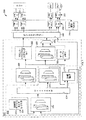
1つ又はそれ以上の被試験デバイス(被試験デバイス203)を試験するための本発明の一実施形態によるマルチタスクAPG201を有する試験システム又はテスター200を、ここで図1を参照して以下に説明する。被試験デバイス203により、任意の電子構成要素モジュール、又は、論理回路、メモリアレイ、又はその両方を有するICを意味する。被試験デバイス203は、例えば、ダイ及びパッケージとすることができ、又は、基板上のいくつかのデバイスの1つとすることができる。被試験デバイス203は、いくつかのピン231を通じて又は基板(図示しない)上のパッドを接続するプローブ(図示しない)を通じて試験システム200に結合することができる。ただ1つの被試験デバイスが示されているが、試験システム200は、複数の被試験デバイス203を並行試験するのに十分に大きないくつかの試験サイトを含むことができ、また、好ましくはそれを含むことが認められるであろう。
The present invention relates to a system and method for efficiently and rapidly testing an integrated circuit (IC) using a tester having a multitask algorithmic pattern generator (APG).
A test system or
明確にするために、公知で本発明に関連のないテスターの詳細の多くは省略されている。テスターは、例えば、本出願人に譲渡されて現在特許申請中の「二重データ速度ピンスクランブルを有する半導体試験システム」という名称の2001年6月29日出願の米国特許出願一連番号第09/895,439号、「半導体デバイスを試験するためのパターンスクランブラーを有する装置及びそれを作動する方法」という名称の2002年1月4日出願の米国特許出願一連番号第10/039,738号、及び「スタック可能半導体試験システム及びそれを作動する方法」という名称の2002年6月12日出願の米国特許出願一連番号第10/170,916号に更に詳細に説明されており、その各々の全内容は、本明細書において引用により組み込まれている。 For clarity, many of the details of testers that are known and not relevant to the present invention have been omitted. The tester is, for example, U.S. Patent Application Serial No. 09/895, filed June 29, 2001, entitled "Semiconductor Test System with Dual Data Rate Pin Scramble" assigned to the present applicant and currently pending. 439, U.S. Patent Application Serial No. 10 / 039,738 filed January 4, 2002, entitled "Apparatus with Pattern Scrambler for Testing Semiconductor Devices and Method of Operating the Same", and This is described in more detail in US Patent Application Serial No. 10 / 170,916, filed June 12, 2002, entitled “Stackable Semiconductor Test System and Method of Operating It”, the entire contents of each Are incorporated herein by reference.
図1を参照すると、テスター200は、一般的に、マルチタスクAPG201に加えて、ピン・スクランブラー240、いくつかのタイミング・ジェネレータ及びフォーマット回路(T/F250)、及びT/Fと被試験デバイス203のピン231との間に結合したいくつかのピン・エレクトロニクス(PE)回路又はチャンネル251を含む。試験サイトコンピュータ(図示しない)及びクロックは、クロックサイクルを有するタイミング又はクロック信号を供給するため及びその作動を制御するために、マルチタスクAPG201内の他の全ての構成部品又は要素、ピン・スクランブラー240、及びT/F250に結合する。
Referring to FIG. 1, a
ピン・スクランブラー回路240は、マルチタスクAPG201のいくつかの出力のいずれか、及びT/F250のいずれかに結合し、T/Fを通じていずれかの被試験デバイス203上のピン231のいずれかに結合する。ピン・スクランブラー240の機能は、被試験デバイス203のピン231のいずれもが各クロックサイクルでAPG201内のどのパターンソースからも駆動されることを可能にすることである。更に、被試験デバイス203の各ピン231に結合したマルチタスクAPG201の出力は、サイクル毎に決めるか又は選択することができる。すなわち、マルチタスクAPG201からの試験信号又はパターンは、特定の被試験デバイス203上の特定のピン231に結合することができ、被試験デバイスへの接続の再配線又はマルチタスクAPG201の大規模な再プログラミングなしにオンザフライで切り換えるか又は変えることができる。図1に示すテスター200では、ピン・スクランブラー240は、マルチタスクAPG201によって制御され(制御用の接続は示していない)、例えば、サイクル毎に被試験デバイス203の各ピン231上の64の異なるパターンマッピングを可能にするように設計することができる。ピン・スクランブラー240を有するテスター200は、米国カリフォルニア州サンホセ所在のネクステスト・システムズ・インコーポレーテッドから市販されており、より詳細には、本出願人に譲渡されて現在申請中の米国特許出願一連番号第09/895,439号に説明されている。
The
T/F250は、試験パターンの様々な信号、すなわち、マルチタスクAPG201から受信した駆動/予測データ信号、ストローブ制御信号、及び入力/出力(I/O)制御信号のタイミング及びフォーマット設定を調節し、マルチタスクAPGからの出力をPEチャンネル251を通じて被試験デバイス203に結合する。
各PEチャンネル251は、一般的に、試験パターン又は信号の3ビット部分をマルチタスクAPG201からT/F250を通じて受け取り、各3ビット信号は、駆動/予測データ信号、ストローブ制御信号、及びI/O制御信号を含む。いくつかの試験システムは、これらの(典型的には)3ビットを8つのPE制御機能の組合せに符号化する。各PEチャンネル251は、一般的に、信号を被試験デバイス203のピン231に結合することができるPEドライバ(図示しない)、出力信号を予測出力信号と比較するための比較器(図示しない)、及び比較の結果をマルチタスクAPG201を通じてエラー捕捉RAM260に再度結合するためのエラー論理回路(図示しない)を含む。一般的に、PEドライバ及び比較器は、ピン231がデータ又は制御信号を受信するか又は所定の時間に結果を送信するかのいずれかであるから、PEチャンネル251においては同時に作動しない。
The T /
Each
マルチタスクAPG201は、制御部分205、レジスタベースのアルゴリズミック・アドレス・ジェネレータ220、アドレス・トポロジカル・スクランブラー222、データ・ジェネレータ230、及びデータマルチプレクサ234を含む。マルチタスクAPG201は、デッドサイクルなしに作動の全てのクロックサイクル毎にデータパターンを生成する能力を有し、デッドサイクルとは、マルチタスクAPGは計算するが、被試験デバイス203に対してデータを何も発生しないサイクルである。データパターンにデッドサイクルがないということは、被試験デバイス203がその最も厳しいタイミング限界で実施されるので、最も厳しい試験を受けることを意味する。デッドサイクルは、より緩い試験をもたらすであろう。更に、デッドサイクルは、試験時間を増大させる。
Multitask
マルチタスクAPG201の制御部分205は、マルチタスクAPG、ピン・スクランブラー240、T/F250、及びPEチャンネル251の作動を制御し、MicroRAMアドレスレジスタ202、MicroRAM204、ループカウンタ及びスタックレジスタ又はレジスタベースのループカウンタ及びスタック210、分岐論理回路212、及び被試験デバイスタスクレジスタ280のようなタスクセレクタから成ることができる。制御部分205は、実行が開始されるとそれ自体を制御する閉ループシステムである。通常の作動では、テスター200のユーザは、ホストコンピュータ(図示しない)によってMicroRAM204に読み込まれるアルゴリズム的パターンを書き込む。MicroRAM204は、一般的に、幅が100から200ビットであり、深さが数百から数万ワードである。MicroRAM204からのビットのいくつかは、マルチタスクAPG201のプログラムの流れを制御し、同時にMicroRAMからの他のビットは、被試験デバイス203に対するデータパターンを発生するレジスタを制御する。
The
MicroRAM204にユーザ書き込みプログラムがロードされた状態で、マルチタスクAPG201は、クロックを発生させることにより実行が開始される。MicroRAMアドレスレジスタ202は、実行される次の命令を指すようにMicroRAM204をアドレス指定する。MicroRAM204は、制御ビットをループカウンタ及びスタック210と分岐論理回路212とに出力する。ループカウンタ及びスタック210は、分岐論理回路212と共に、MicroRAMアドレスレジスタ202の中にロードする次のMicroRAMアドレスを判断する。ループカウンタは、カウント値に達するまで命令を実行させ、次に、分岐論理回路212は、新しいMicroRAMアドレスレジスタ値をロードする。スタックは、サブルーチンが実行された時に、戻りMicroRAMアドレスを供給する。分岐論理回路212は、一般的に、上述のループカウンタを含む様々な条件に基づいて、ジャンプ、サブルーチンコール、及びサブルーチンリターンを可能にする。パターンを実行するこの処理は、分岐論理回路212がマルチタスクAPG201の停止専用のMicroRAM204ビットコードにより中断するように命令されるまで続けられる。
With the user write program loaded in the
制御部分205が上述のように実行されている間、MicroRAM204からの追加のビットは、被試験デバイスアドレス、被試験デバイスデータ、及び恐らくは他の機能をアルゴリズム的に発生させるために、マルチタスクAPG201の他の部分に同時に送られている。図1は、MicroRAM204によって駆動されているレジスタベースのアルゴリズミック・アドレス・ジェネレータ220を示している。アドレス・ジェネレータ220の出力は、アドレス・トポロジカル・スクランブラー222及びデータ・ジェネレータ230を駆動する。アドレス・トポロジカル・スクランブラー222は、一般的にランダム・アクセス・メモリであり、これは、トポロジー的に真のデータパターンを、被試験デバイス203のピン231に印加されたアドレスをしばしばスクランブル処理する被試験デバイスのアドレス符号器(図示しない)に通した後に、被試験デバイスの内部アレイ(図示しない)に供給する。
While the
レジスタベースのデータ・ジェネレータ230は、被試験デバイス203に対するデータパターンをアルゴリズム的に発生し、アドレス・ジェネレータ220によって送られるアドレスに基づいて、パターンを条件付で反転させることができる。アルゴリズム的データに加えて、いくつかの被試験デバイス203は、記憶された応答データパターンを被試験デバイスアドレスの関数として要求する。この例は、データパターンが永久的に被試験デバイス203内にプログラムされる読出し専用メモリ(ROM)であろう。データバッファメモリ232は、ランダム・アクセス・メモリであり、これは、アドレス・ジェネレータ220からのアドレスの関数として供給された記憶応答データパターンを保持する。MicroRAM204を通じての試験プログラムは(制御用の接続は示していない)、どのデータソースがデータマルチプレクサ234を通して被試験デバイスに送られるかを制御することができる。
図1に示すテスター200は、アドレス・トポロジカル・スクランブラー222、データマルチプレクサ234、及び他のマルチタスクAPGデータソースの出力をピン・スクランブラー240を通じて経路指定する。
The register-based
The
microRAMアドレスレジスタ202、ループカウンタ及びスタック210、アドレス・ジェネレータ220、及びデータ・ジェネレータ230で使用するためのストレージ構成要素又はレジスタを、ここで図2を参照して以下に更に詳細に説明する。図2は、本発明のマルチタスクAPG201で使用するためのマルチタスクAPGストレージ構成要素又はレジスタ270の実施形態のブロック図である。本発明によると、マルチタスクAPGレジスタ270は、n個のストレージ要素又はレジスタ272、273、及び274と、レジスタ272、273、及び274から供給されるマルチプレクサ276のようなセレクタ要素又は機構とで構成される。各レジスタ272、273、及び274は、マルチプレクサの選択と同期した別々のクロックイネーブル(図示しない)を有する。例えば、マルチプレクサ276が第1の入力を選択する時は、第1のレジスタ272のクロックだけが使用可能にされる。マルチプレクサがn番目の入力を選択する時は、n番目のレジスタ274のクロックだけが使用可能にされる。すなわち、マルチタスクAPG201内のレジスタ272、273、及び274は、各被試験デバイス203に対して別々の値を保持することができる。
The storage components or registers for use in the
本発明のマルチタスクAPG201は、遅い速度の作動に対して独立したAPG機能を与えることにより、ピン数の少ない被試験デバイス203を試験するためのテスター200のハードウエアコストを低減する。高速作動が必要な時は、被試験デバイスを最大APG速度のロックステップで作動し、処理量を最大にして、低速APGが与えるものよりも厳しい試験条件を提供することができる。すなわち、フラッシュメモリのような被試験デバイス203をプログラムする際には、マルチタスクAPG201は、試験パターンが被試験デバイスをプログラムするのに必要である限りにおいてのみ各被試験デバイスに対して独立にブロードキャストされるか又は書き込まれるマルチタスクモードで作動される。対照的に、プログラミングに適用される従来のテスターは、最後の最も遅い被試験デバイスがプログラムされるまで、全ての被試験デバイスに対して同時にパターンを試験する。試験パターンを各被試験デバイス203に書き込むことは、それ独自でいくつかの有益な効果をもたらす。第1に、所定の期間により多数の被試験デバイス203の並行試験を可能にすることによってテスター200の処理量を最大にするマルチタスクAPG201リソースのより効率的な利用法が存在する。これは、プログラミングが、一般的に、いくつかのパターンを各被試験デバイス203に書き込むことを伴うからである。例えば、いくつかの被試験デバイス203を並行にプログラムすることは、デバイスのメモリセルを覆って対角線状パターンを各被試験デバイスに書き込み、次に、いくつかの縞を書き込むことを含むであろう。すなわち、より迅速にプログラムする被試験デバイス203に対しては、テスターは、最も遅い被試験デバイスが対角線状パターンをプログラムするのを待つのではなく、以前にプログラムされた対角線状パターンの上への縞パターンの書き込みを始めることができる。第2に、プログラミング信号又は試験パターンは、被試験デバイスをプログラムすることが必要であるかぎりにおいてのみ各被試験デバイス203に適用されるので、各被試験デバイスは、デバイスに対する閾値をちょうど超えた蓄積電荷を使用してプログラムされ、その後の被試験デバイス電荷又はプログラム保持能力の試験は、より高い初期電荷で開始した被試験デバイスのいくつかによる誤ったポジティブな結果を生み出す可能性が低いことになる。
The
全ての被試験デバイス203が問題なくプログラムされた後で、マルチタスクAPG201は、プログラムされたパターンを全ての被試験デバイスから同時に読み戻すために最大APG速度のロックステップで作動され、それによって処理量を最大にすることができる。
上述の通り、フラッシュメモリは、それらの読取サイクルに比べて非常に遅い速度でプログラムする。すなわち、プログラミング中は、APGは、一般的に遅いサイクル速度で作動する。この事実を利用して、ハードウエアを時間多重化して出力を適切な被試験デバイスに誘導することにより、また、各被試験デバイス又はタスクに対してAPG時間をタイム・シェアリング又はタイムスライスすることにより、高速マルチタスクAPG201を複数の独立したより遅いAPGに見えるようにすることができる。例えば、20ナノ秒のサイクル速度で作動するAPGは、連続するサイクルにおいて4つの被試験デバイスの各々を順次駆動することができるであろう。第1の被試験デバイスは、情報が計算されて最初の20ナノ秒サイクルで起動され、第2の被試験デバイスは、2番目の20ナノ秒サイクルで、第3の被試験デバイスは、3番目の20ナノ秒サイクルで、第4の被試験デバイスは、4番目の20ナノ秒サイクルで起動される。最初の被試験デバイスに再度戻った時には80ナノ秒が過ぎており、従って、第1の被試験デバイスは、80ナノ秒の有効サイクル時間を見ることになり、他の被試験デバイスの各々も、時間が交互するが同様である。
After all devices under
As described above, flash memory programs at a very slow rate compared to their read cycle. That is, during programming, the APG generally operates at a slow cycle rate. Taking advantage of this fact, time sharing or time slicing the APG time for each device or task under test by multiplexing the hardware to direct the output to the appropriate device under test Thus, the high-
これは、従来技術のAPGに使用される従来のレジスタがレジスタのようなマルチタスクAPGストレージ構成要素270によって置き換えられた図1に見ることができる。MicroRAMアドレスレジスタ202、ループカウンタ及びスタック210、アドレス・ジェネレータ220、データ・ジェネレータ230は、全てマルチタスクAPG201におけるマルチタスクAPGレジスタ270である。これらのマルチタスクAPGレジスタ202、210、212、及び220は、どの被試験デバイス203がアクティブなタイムスライスにおいて検査を行うかを指定する被試験デバイスタスクレジスタ280のようなタスクセレクタから制御を受ける。被試験デバイスタスクレジスタ280には、マルチタスクモードで検査を受けることになる被試験デバイスの数を含む情報がホストコンピュータ(図示しない)から入力又はコンピュータバス281を通じてロードされる。
This can be seen in FIG. 1 where conventional registers used in prior art APGs have been replaced by multi-task
一実施形態では、被試験デバイスタスクレジスタ280は、基本的には、検査を受ける被試験デバイス203の数をnとする時に1からnまで計数するカウンタである。被試験デバイスタスクレジスタ280の出力は、バイナリコード、n個の独立したイネーブルの組、又は、何らかの他のフォーマット又はフォーマットの組合せとしてブロードキャストすることができる。
代替的に、被試験デバイスタスクレジスタ280は、サイクル速度(周期)と、被試験デバイス203が試験されるサイクル開始時間又は順番と、各被試験デバイスに適用される試験パターンとを独立に検査することができるインテリジェントコントローラである。すなわち、各被試験デバイス203は、その独自の周期(サイクル速度)を有することができ、各被試験デバイスサイクルの始めは、時間が交互していない(又は、交互する必要はない)。被試験デバイスサイクルの始めは、他の被試験デバイスに対するタイミングに関わらず、時間のどこからでも起こる可能性がある。この実施形態では、被試験デバイスタスクレジスタ280は、各被試験デバイス203に対して次に来るサイクルの周期を見て、所定の判断基準に基づき(i)次に来るサイクルでどの被試験デバイスがマルチタスクAPG201を使用するようになるか、及び(ii)その特定の被試験デバイスに対してT/F250を通じて何時データを伝達させるかを決めることができるインテリジェントコントローラである。所定の判断基準は、例えば、データをT/F250に伝達させるためのリアルタイムで変化する可変長さのパイプラインと、各被試験デバイス203のサイクル速度又は周期とを含むことができる。この実施形態の1つの好ましいバージョンでは、被試験デバイスタスクレジスタ280は、3ビットコードではなくT/F250に対する別々のイネーブルを使用し、それによってデータが必要に応じて各被試験デバイスに独立に移動することを可能にする。
In one embodiment, the device under test task register 280 is basically a counter that counts from 1 to n, where n is the number of devices under
Alternatively, the device under test task register 280 independently examines the cycle rate (period), the cycle start time or sequence in which the device under
従来技術のAPGにおけるように、マルチタスクAPG201は、アルゴリズム的にパターンを計算するために、著しい量の組合せ論理回路及びRAMを含む。また、アドレス・トポロジカル・スクランブラー222及びデータバッファメモリ232にも、かなりのRAMがある。組合せ論理回路又はRAMのいずれもマルチタスクAPG201内で反復されず、それによってかなりのハードウエアコストを節約する。
As in the prior art APG, the
被試験デバイスタスクレジスタ280はまた、ピン・スクランブラー240及びT/F250に接続される。タイミングが取られフォーマット設定された信号は、被試験デバイスに到達する前の正確な電圧調整のためにピン・エレクトロニクス・チャンネル(P/E251)を通過する。ピン・エレクトロニクス・チャンネル251は、一般的に、試験ベクトルやデータを被試験デバイス203のピンに印加するためのPEドライバ、被試験デバイス出力信号を予測出力信号と比較するための比較器、及び比較結果をエラー捕捉メモリ又はエラー捕捉RAM260に再度結合するためのエラー論理回路を含む。
The device under test task register 280 is also connected to the
APG201内のこの点では、信号は、被試験デバイス203あたりのピンレベルで分離される。ピン・スクランブラー240は切り換わることができるが、被試験デバイスタスクレジスタ280は、タイミング・ジェネレータ及びフォーマット設定器250に対して、計時してアクティブな被試験デバイスに対してのみ送信するように命令することになる。非アクティブな被試験デバイス203上のタイミング・ジェネレータ及びフォーマット設定器250は、新しいデータをラッチするためのイネーブルを受け取らないことになり、従って、それらが行っていた作動がどれであれ、それを継続することになる。
At this point in the
エラー捕捉RAM260は、エラー捕捉メモリのどの部分をエラー記録のために使用するかを教える被試験デバイスタスクレジスタ280信号を受け取る。エラー捕捉RAM260は、単に、被試験デバイスタスクレジスタ280をポインタとして用いて被試験デバイス203毎に再分割することができる大型ランダム・アクセス・メモリである。
マルチタスクAPG201は、テスター200が単一のパターン・ジェネレータ上で複数のプログラムを同時に実行することを可能にする。プログラムを同時に実行する間、マルチタスク作動システムは、マルチタスクAPG201作動をタイムスライスし、プログラムが終了するまで、連続ループで小さな時間区分の間、各プログラムに対してマルチタスクAPGリソースを与える。プログラムに対する処理は、時間的にインターリーブされる。
The
Multitask
一実施形態では、マルチタスクAPG201のハードウエア又はリソースは、最大8つの経路にタイムスライスされ、最大8つの試験プログラムが、単一APG上で独立かつ同時に実行されることを可能にする。例えば、マルチタスクAPG201を有するテスター200の128ピン試験サイトは、最大8つの経路に分割され、最大8つの独立した16ピンの被試験デバイス試験サイトをもたらす。各16ピン被試験デバイス試験サイトに対するタイミング及びフォーマット設定は、T/F250を通じて独立に分配される。
In one embodiment, the
マルチタスクAPG201が試験信号又はパターンを被試験デバイス203にブロードキャストする準備ができた時は、その被試験デバイスのみ(他の被試験デバイスではなく)に付随する試験サイト上のタイミングシステムがロードされる。この試験サイトのタイミングシステム又はT/F250がこのロードした被試験デバイスサイクルを実行している間に、マルチタスクAPG201は、引き続いて他の被試験デバイスサイトに対して同じことを行う。
When the
マルチタスク機能は、パターン実行におけるいかなるデッドサイクルも発生させない。パターンは、ちょうど従来のAPG上で実行されるように実行される。ユーザは、従来のAPGを用いて行うように、ホストコンピュータ(図示しない)からマルチタスクAPG201に全ての試験パターンを書き込み、マルチタスク・ハードウエアのどれも管理する必要はない。ユーザが認識する必要がある唯一のものは、試験される被試験デバイス203の数又はマルチタスクAPG201リソースが分割される時間領域、及びマルチタスクモードで利用可能な最大サイクル時間である。
The multitasking function does not cause any dead cycle in pattern execution. The pattern is executed just as it is executed on a conventional APG. The user writes all test patterns from the host computer (not shown) to the
並行して試験される被試験デバイス203の数又は時間領域がマルチタスクモードにおいて増加すると、特定の被試験デバイス又は試験サイトでの最大サイクル速度が減少する。これは、試験サイトの増加がマルチタスクAPG201からより多くのタイムスライスを要求し、全てのプログラムを処理するのにより多くの合計時間がかかるからである。これは、被試験デバイスアレイ読み取りに対して被試験デバイスプログラミングに必要なサイクル時間とサイトの独立性との性質から、フラッシュメモリ試験に対しては恩典である。
As the number or time domain of devices under
一実施形態では、マルチタスクAPG201は、20ナノ秒周期である50MHzの最大サイクル速度を有する。以下の表1は、被試験デバイスサイト上で利用可能な例示的な最大サイクル速度をマルチタスクされる被試験デバイスの数に対して示すものである。
In one embodiment,

遅いサイクル速度でのフラッシュメモリプログラミングに対しては、マルチタスクを用いて独立の被試験デバイスサイトによる最大の処理量を達成することができる。高速の被試験デバイスアレイ読み取り(より高速のためにより高い処理量を意味する)に対しては、被試験デバイスサイトは、最大50MHzのロックステップで実行することができる。すなわち、このようなマルチタスクAPGは、独立した16ピンの被試験デバイスサイトを、従来の並行試験モードでの最大6.25MHz及び最大50MHzの作動で全て1つのハードウエアから供給する。 For flash memory programming at slow cycle rates, multitasking can be used to achieve maximum throughput with independent device under test sites. For high-speed device-under-test array reads (meaning higher throughput due to higher speed), the device-under-test site can be run with up to 50 MHz lockstep. That is, such a multitasking APG provides independent 16-pin device under test sites all from one piece of hardware with up to 6.25 MHz and up to 50 MHz operation in conventional parallel test mode.
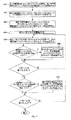
第1及び第2の被試験デバイス203を試験するための処理又は方法の実施形態を、ここで図3を参照して以下に説明する。図3は、いくつかの被試験デバイス203に対してマルチタスクモードで並行して書き込むか又はプログラムするマルチタスクAPG201を有するテスターを作動するための処理の実施形態を示す流れ図である。
図3を参照すると、処理は、被試験デバイス203を試験するためのいくつかのビットを含む試験信号又はパターンをマルチタスクAPG201にロードすることにより始まる(段階300)。これは、ホストコンピュータからMicroRAMアドレスレジスタ202及び被試験デバイスタスクレジスタ280へ、それぞれコンピュータバス282及びコンピュータバス281を通じてロードすることにより達成される。一般的に、これは、試験パターンをMicroRAMアドレスレジスタ202に、また、マルチタスクAPG201が分割されることになる時間領域の数と各時間領域において検査を受けることになる被試験デバイスのPEチャンネルの数及びアイデンティティとを含む情報を被試験デバイスタスクレジスタ280にロードする段階を伴う。次に、第1の試験パターンは、いくつかの時間領域の最初の時間領域において、被試験デバイス203の少なくとも1つの第1の組に結合されるか又はそれに供給される(段階305)。試験パターンは、1ビットからPEチャンネル251又は被試験デバイス203上のピン231の数に等しい幅までの幅を有することができる。第1の試験パターンが関連T/F250を通じて第1の組の被試験デバイス203に完全に供給された後に、第1の試験パターンは、第1の組の被試験デバイスから分離されるか又は取り除かれ(段階310)、第2の試験パターンが、第2の時間領域において第2の組の被試験デバイスに結合されるか又はそれに供給される(段階315)。ここでもまた、第2の試験パターンが関連T/F250を通じて第2の組の被試験デバイス203に完全に供給された後に、第2の試験パターンは、第2の組の被試験デバイスから分離されるか又は取り除かれ(段階320)、第1及び第2の試験パターン全体が第1及び第2の組の被試験デバイスに印加されるか又は供給されるまで、すなわち、全ての被試験デバイス203が完全にプログラムされるまで、段階305から320が繰り返される(段階325)。
An embodiment of a process or method for testing the first and second devices under
Referring to FIG. 3, the process begins by loading a
第1及び第2の被試験デバイス203を試験するための処理又は方法の実施形態を、ここで図4を参照して以下に説明する。図4は、いくつかの被試験デバイス203に対してマルチタスクモードで並行して書き込むか又はプログラムするマルチタスクAPG201を有するテスターを作動するための処理の実施形態を示す流れ図である。
図4を参照すると、処理は、いずれもその第1のサイクルを開始する第1の時間領域における1つ又はそれ以上の被試験デバイス203(被試験デバイス1)と、第2の時間領域における1つ又はそれ以上の被試験デバイス(被試験デバイス2)とによって始まる(段階401)。現在の被試験デバイス1/2サイクルの第1のタイムスライスを用いて、次の被試験デバイス1サイクルに対するデータを転送する(段階402)。全てのタイムスライスは、20ナノ秒の持続時間を有する。現在の被試験デバイス1/2サイクルの第2のタイムスライスを用いて、次の被試験デバイス2サイクルに対するデータを転送する(段階403)。次の被試験デバイス1又は(被試験デバイス1及び被試験デバイス2)は、新しいサイクルを開始する(段階404)。新しいサイクルの第1のタイムスライスを用いて、次の被試験デバイス1サイクルに対するデータを転送する(段階405)。被試験デバイス2が被試験デバイス1と同時にその新しいサイクルを開始した場合、第2のタイムスライスを用いて、次の被試験デバイス2サイクルに対するデータを転送する(段階406)。パターンが終了していない場合は、段階404〜406を繰り返す。それ以外は、被試験デバイス1及び被試験デバイス2サイクルの長さが符合せず、スライスの割り振りは、この時点では被試験デバイス数ではなく優先順位に基づくことになり、すなわち、コントローラである被試験デバイスタスクレジスタ280は、実際に本実施形態のカウンタのようには見えない。被試験デバイス2が被試験デバイス1の前に新しいサイクルを開始した場合、第1の利用可能なスライス(この例では、前のスライスの開始後少なくとも20ナノ秒として定義された)を用いて、次の被試験デバイス2サイクルに対するデータを転送する(段階406)。パターンが完了しない場合は、段階407を繰り返し、それ以外は段階404へ進む。
An embodiment of a process or method for testing the first and second devices under
Referring to FIG. 4, the process includes one or more devices under test 203 (device under test 1) in the first time domain and 1 in the second time domain, all of which begin its first cycle. Beginning with one or more devices under test (device under test 2) (step 401). Using the first time slice of the current device under
被試験デバイスタスクレジスタ280がストレージ要素272、273、及び274のいずれかを選択して特定時間領域内の被試験デバイス203に結合させ、その時間領域内の被試験デバイスの各々を個々に使用可能にすることができるために、異なる時間領域の被試験デバイスに書き込まれた試験パターンは同じである必要はなく、各時間領域の期間も同じである必要はないことが理解されるであろう。例えば、一実施形態では、マルチタスクAPG201は、特定時間領域の全ての被試験デバイス203が何時プログラムされたかを認識して、試験パターンが残りの時間領域の被試験デバイスに結合される周期又は周波数を調節し、それによってテスター200の効率を最大にすることができる。更に、被試験デバイス203又は時間領域は、規則的又は連続的に交互する順番で検査を受ける必要はなく、優先順位に基づいて必要な任意の順番で被試験デバイス又は時間領域に検査を提供するためにストレージ要素272、273、及び274のいずれかを選択することができる。例えば、サイクル時間が80ナノ秒、100ナノ秒、80ナノ秒、及び200ナノ秒である次に来るサイクルを有するか又はそれを要求する4つの時間領域において複数の被試験デバイスが試験される場合、被試験デバイスタスクレジスタ280は、ストレージ要素272、273、及び274を選択し、被試験デバイスに対して第1の時間領域、次に第3の時間領域、第2の時間領域、最後に第4の時間領域で検査を提供することができる。更に、試験の順番は、その次に来るサイクルで変えることができる。
任意的に、同じ試験パターンが異なる時間領域の全ての被試験デバイスに書き込まれるか又はプログラムされた時、本方法は、マルチタスクAPG201をロックステップで作動して全ての被試験デバイスに結合させ、試験パターンをマルチタスクAPGの最大周波数又は速度で読み戻す付加的な段階を更に含む(段階330)。
The device under test task register 280 selects one of the
Optionally, when the same test pattern is written or programmed to all devices under test in different time domains, the method activates the
本発明の以上の特定実施形態の記述は、例証及び説明のためのものである。それらは網羅的ではなく、また、本発明を開示した正確な形態に限定しないものであり、明らかに、以上の教示に照らして多くの修正及び変形が可能である。実施形態は、本発明の原理及びその実際的応用を最もよく説明し、それによって当業者が本発明と想定される特定の用途に適するような修正を有する様々な実施形態とを最もよく使用することができるように選ばれて説明されたものである。本発明の範囲は、本明細書に添付した特許請求の範囲及びその均等物によって規定されるものとする。 The foregoing descriptions of specific embodiments of the present invention are for purposes of illustration and description. They are not exhaustive and do not limit the invention to the precise form disclosed, and obviously many modifications and variations are possible in light of the above teaching. The embodiments best explain the principles of the invention and its practical application, and thereby best use various embodiments with modifications so that those skilled in the art will be able to fit the invention and the particular application envisioned. It is chosen and explained so that it can be. It is intended that the scope of the invention be defined by the claims appended hereto and their equivalents.
200 試験システム又はテスター
201 マルチタスク・アルゴリズミック・パターン・ジェネレータ(APG)
203 被試験デバイス
204 MicroRAM
212 分岐論理回路
222 アドレス・トポロジカル・スクランブラー
232 データバッファメモリ
280 被試験デバイスタスクレジスタ
200 Test system or
203 Device under
212
Claims (20)
第1の半導体デバイスに結合するように構成された第1の組のピン、及び第2の半導体デバイスに結合するように構成された第2の組のピンと、
前記第1の組のピンに結合した少なくとも1つの第1のシグナルジェネレータ、及び前記第2の組のピンに結合した少なくとも1つの第2のシグナルジェネレータと、
前記少なくとも1つの第1のシグナルジェネレータと前記少なくとも1つの第2のシグナルジェネレータとに結合し、前記第1の半導体デバイスに関連するデータを収容する第1のストレージ要素と前記第2の半導体デバイスに関連するデータを収容する第2のストレージ要素とを有するストレージ構成要素と、
前記第1の半導体デバイスが検査を受けている時に、処理及び誘導のためにアクセスされている前記第1のストレージ要素からデータを前記第1の組のピンまで誘導し、前記第2の半導体デバイスが検査を受けている時に、処理及び誘導のためにアクセスされている前記第2のストレージ要素からデータを前記第2の組のピンまで誘導するための、前記ストレージ構成要素に結合したタスクセレクタと、
を含むことを特徴とする装置。 A multitasking apparatus for testing first and second semiconductor devices,
A first set of pins configured to couple to the first semiconductor device, and a second set of pins configured to couple to the second semiconductor device;
At least one first signal generator coupled to the first set of pins and at least one second signal generator coupled to the second set of pins;
A first storage element coupled to the at least one first signal generator and the at least one second signal generator to receive data associated with the first semiconductor device and the second semiconductor device; A storage component having a second storage element containing associated data;
Directing data from the first storage element being accessed for processing and guidance to the first set of pins when the first semiconductor device is undergoing inspection; and the second semiconductor device A task selector coupled to the storage component for directing data from the second storage element being accessed for processing and navigation to the second set of pins when ,
The apparatus characterized by including.
前記少なくとも1つの第2のシグナルジェネレータは、前記第2の組のピンの各ピンに結合した第2のシグナルジェネレータを含み、
前記ストレージ構成要素は、前記第1及び第2のシグナルジェネレータの各々に結合される、
ことを特徴とする請求項1に記載の装置。 The at least one first signal generator includes a first signal generator coupled to each pin of the first set of pins;
The at least one second signal generator includes a second signal generator coupled to each pin of the second set of pins;
The storage component is coupled to each of the first and second signal generators;
The apparatus according to claim 1.
前記タスクセレクタは、前記第1の半導体デバイスが検査を受けている時に、処理及び誘導のためにアクセスされている前記第1のストレージ要素から前記付加的なデータを前記第1の組のピンまで誘導し、前記第2の半導体デバイスが検査を受けている時に、処理及び誘導のためにアクセスされている前記第2のストレージ要素から該付加的なデータを前記第2の組のピンまで誘導するために前記付加的なストレージ構成要素に結合される、
ことを特徴とする請求項1に記載の装置。 An additional storage element that contains additional data associated with the first semiconductor device and a second storage element that accommodates additional data associated with the second semiconductor device. Further including a storage component;
The task selector transfers the additional data from the first storage element being accessed for processing and guidance to the first set of pins when the first semiconductor device is undergoing inspection. And directing the additional data from the second storage element being accessed for processing and guidance to the second set of pins when the second semiconductor device is undergoing inspection. Coupled to the additional storage component for
The apparatus according to claim 1.
複数の半導体デバイスに結合するようになったマルチタスク・アルゴリズミック・パターン・ジェネレータ(APG)、
を含み、
前記マルチタスクAPGは、第1の時間領域において前記複数の半導体デバイスの第1のものに第1の試験パターンを供給し、第2の時間領域において該複数の半導体デバイスの第2のものに第2の試験パターンを供給するように構成される、
ことを特徴とする装置。 A test apparatus for testing a plurality of semiconductor devices,
Multitask algorithmic pattern generator (APG), which is now coupled to multiple semiconductor devices
Including
The multitasking APG supplies a first test pattern to a first one of the plurality of semiconductor devices in a first time domain and a second one of the plurality of semiconductor devices in a second time domain. Configured to provide two test patterns;
A device characterized by that.
MicroRAMアドレスレジスタ、
ループカウンタ及びスタックレジスタ、
アドレス・ジェネレータ、及び
データ・ジェネレータ、
から成る群から選択されたレジスタを含むことを特徴とする請求項8に記載の試験装置。 The multitasking APG is
MicroRAM address register,
Loop counter and stack register,
Address generator and data generator,
The test apparatus of claim 8, comprising a register selected from the group consisting of:
前記被試験デバイスタスクレジスタは、前記第1の時間領域において前記複数の半導体デバイスの前記第1のものに結合される前記いくつかのストレージ要素の1つと、前記第2の時間領域において前記複数の半導体デバイスの前記第2のものに結合される前記いくつかのストレージ要素の1つとを選択するようになっている、
ことを特徴とする請求項8に記載の試験装置。 The multitasking APG further includes a device under test task register coupled to the at least one register;
The device under test task register includes one of the plurality of storage elements coupled to the first one of the plurality of semiconductor devices in the first time domain and the plurality of the plurality of semiconductor elements in the second time domain. Selecting one of the several storage elements coupled to the second one of the semiconductor devices;
The test apparatus according to claim 8.
前記被試験デバイスタスクレジスタは、前記第1の時間領域において前記複数の半導体デバイスの前記第1のものに結合したT/F及びPEチャンネルのみ、及び前記第2の時間領域において前記複数の半導体デバイスの前記第2のものに結合したT/F及びPEチャンネルのみを使用可能にするようになっている、
ことを特徴とする請求項11に記載の試験装置。 A plurality of timing and formatting circuits (T / F) and a pin electronics (PE) channel through which each of the plurality of semiconductor devices is coupled to the number of storage elements;
The device under test task register includes only T / F and PE channels coupled to the first of the plurality of semiconductor devices in the first time domain, and the plurality of semiconductor devices in the second time domain Only the T / F and PE channels coupled to the second one of
The test apparatus according to claim 11.
i.APGからの第1の試験パターンの少なくとも一部分を、nを1よりも大きい整数とした時にn個のいくつかの時間領域の第1のものにおける複数の半導体デバイスの少なくとも1つの第1の組に供給する段階と、
ii.前記APGからの前記第1の試験パターンを前記複数の半導体デバイスの前記第1の組から取り除く段階と、
iii.前記APGからの第2の試験パターンの少なくとも一部分を、第2の時間領域における前記複数の半導体デバイスの少なくとも1つの第2の組に供給する段階と、
iv.前記APGからの前記第2の試験パターンを前記複数の半導体デバイスの前記第2の組から取り除く段階と、
v.全ての第1及び第2の試験パターンが前記第1及び第2の複数の半導体デバイスに印加されるまで、段階iからivを繰り返す段階と、
を含むことを特徴とする方法。 A method for testing a plurality of semiconductor devices using a test apparatus having a multitask algorithmic pattern generator (APG), comprising:
i. At least a portion of the first test pattern from the APG is applied to at least one first set of semiconductor devices in the first of n number of time domains, where n is an integer greater than 1. Supplying, and
ii. Removing the first test pattern from the APG from the first set of the plurality of semiconductor devices;
iii. Providing at least a portion of a second test pattern from the APG to at least one second set of the plurality of semiconductor devices in a second time domain;
iv. Removing the second test pattern from the APG from the second set of the plurality of semiconductor devices;
v. Repeating steps i through iv until all first and second test patterns are applied to the first and second plurality of semiconductor devices;
A method comprising the steps of:
前記第1の試験パターンを複数の半導体デバイスの第1の組に供給する段階は、前記第1の時間領域において前記複数の半導体デバイスの前記第1の組に結合される前記n個のストレージ要素の1つを選択する段階を含む、
ことを特徴とする請求項13に記載の方法。 The multitasking APG includes at least one register having at least n storage elements and a selector element through which the storage elements are coupled to the plurality of semiconductor devices;
Supplying the first test pattern to a first set of semiconductor devices includes the n storage elements coupled to the first set of semiconductor devices in the first time domain. Including selecting one of
The method according to claim 13.
前記第2の試験パターンを複数の半導体デバイスの第2の組に供給する段階は、前記第2の時間領域において前記複数の半導体デバイスの前記第2の組に結合される前記n個のストレージ要素の1つを選択する段階を含む、
ことを特徴とする請求項16に記載の方法。 The multitasking APG includes at least one register having at least n storage elements and a selector element through which the storage elements are coupled to the plurality of semiconductor devices;
Supplying the second test pattern to a second set of semiconductor devices includes the n storage elements coupled to the second set of semiconductor devices in the second time domain. Including selecting one of
The method according to claim 16.
前記第1の試験パターンを複数の半導体デバイスの第1の組に供給する段階は、前記第1の時間領域において該複数の半導体デバイスの該第1の組に結合したT/F及びPEチャンネルのみを使用可能にする段階を含み、
前記第2の試験パターンを複数の半導体デバイスの第2の組に供給する段階は、前記第2の時間領域において該複数の半導体デバイスの該第2の組に結合したT/F及びPEチャンネルのみを使用可能にする段階を含む、
ことを特徴とする請求項13に記載の方法。 The test apparatus further includes a plurality of timing and formatting circuits (T / F) and a pin electronics (PE) channel through which each of the plurality of semiconductor devices is coupled to the n storage elements. ,
Supplying the first test pattern to a first set of semiconductor devices includes only T / F and PE channels coupled to the first set of semiconductor devices in the first time domain; Including the step of enabling
Supplying the second test pattern to a second set of semiconductor devices includes only T / F and PE channels coupled to the second set of semiconductor devices in the second time domain; Including the stage of enabling
The method according to claim 13.
前記複数の半導体デバイスの各々を該複数の半導体デバイスのn組の1つに割り当て、
前記複数の半導体デバイスの前記n組の各々を前記n個の時間領域の1つに関連付ける、
初期段階を更に含むことを特徴とする請求項13に記載の方法。 Specify the number n of time domains,
Assigning each of the plurality of semiconductor devices to one of the n sets of the plurality of semiconductor devices;
Associating each of the n sets of the plurality of semiconductor devices with one of the n time domains;
The method of claim 13 further comprising an initial stage.
Applications Claiming Priority (2)
| Application Number | Priority Date | Filing Date | Title |
|---|---|---|---|
| US37848802P | 2002-05-06 | 2002-05-06 | |
| PCT/US2003/014328 WO2003093845A2 (en) | 2002-05-06 | 2003-05-06 | Semiconductor test system having multitasking algorithmic pattern generator |
Publications (2)
| Publication Number | Publication Date |
|---|---|
| JP2005528596A true JP2005528596A (en) | 2005-09-22 |
| JP2005528596A5 JP2005528596A5 (en) | 2006-05-18 |
Family
ID=29401608
Family Applications (1)
| Application Number | Title | Priority Date | Filing Date |
|---|---|---|---|
| JP2004502010A Pending JP2005528596A (en) | 2002-05-06 | 2003-05-06 | Semiconductor test system with multitask algorithmic pattern generator |
Country Status (5)
| Country | Link |
|---|---|
| US (1) | US7472326B2 (en) |
| JP (1) | JP2005528596A (en) |
| KR (1) | KR101021375B1 (en) |
| TW (1) | TWI278778B (en) |
| WO (1) | WO2003093845A2 (en) |
Cited By (2)
| Publication number | Priority date | Publication date | Assignee | Title |
|---|---|---|---|---|
| JP2006179144A (en) * | 2004-12-24 | 2006-07-06 | Fujitsu Ltd | High-speed test method and device of ic |
| JP2008546063A (en) * | 2005-05-19 | 2008-12-18 | ネクステスト システムズ コーポレイション | System and method for testing a smart card |
Families Citing this family (7)
| Publication number | Priority date | Publication date | Assignee | Title |
|---|---|---|---|---|
| US7913002B2 (en) * | 2004-08-20 | 2011-03-22 | Advantest Corporation | Test apparatus, configuration method, and device interface |
| JP4915779B2 (en) * | 2006-06-02 | 2012-04-11 | 株式会社メガチップス | Connection method between devices and connection device |
| KR20090036144A (en) * | 2006-08-14 | 2009-04-13 | 가부시키가이샤 어드밴티스트 | Test device and test method |
| TWI436077B (en) * | 2010-11-24 | 2014-05-01 | Etron Technology Inc | Method of increasing a chip burn-in scanning efficiency |
| US9514016B2 (en) * | 2011-02-01 | 2016-12-06 | Echostar Technologies L.L.C. | Apparatus systems and methods for facilitating testing of a plurality of electronic devices |
| CN104425269B (en) * | 2013-08-27 | 2017-07-14 | 中芯国际集成电路制造(上海)有限公司 | Fin formula field effect transistor and forming method thereof |
| US10242750B2 (en) * | 2017-05-31 | 2019-03-26 | Sandisk Technologies Llc | High-speed data path testing techniques for non-volatile memory |
Family Cites Families (19)
| Publication number | Priority date | Publication date | Assignee | Title |
|---|---|---|---|---|
| WO1986004686A1 (en) * | 1985-01-31 | 1986-08-14 | Hitachi, Ltd. | Test pattern generator |
| JPH0750159B2 (en) * | 1985-10-11 | 1995-05-31 | 株式会社日立製作所 | Test pattern generator |
| EP0255118B1 (en) * | 1986-07-30 | 1999-06-09 | Hitachi, Ltd. | Pattern generator |
| JPH0754345B2 (en) * | 1986-07-30 | 1995-06-07 | 株式会社日立製作所 | IC test equipment |
| JP2514223Y2 (en) * | 1989-11-07 | 1996-10-16 | ミサワホーム株式会社 | A sash with a sliding shoji |
| US5349587A (en) * | 1992-03-26 | 1994-09-20 | Northern Telecom Limited | Multiple clock rate test apparatus for testing digital systems |
| JPH07198798A (en) * | 1993-12-28 | 1995-08-01 | Hitachi Ltd | Algorithmic pattern generator |
| US5572666A (en) * | 1995-03-28 | 1996-11-05 | Sun Microsystems, Inc. | System and method for generating pseudo-random instructions for design verification |
| CA2213966C (en) | 1995-12-27 | 2004-10-26 | Koken Co., Ltd. | Monitoring control apparatus |
| US5883905A (en) * | 1997-02-18 | 1999-03-16 | Schlumberger Technologies, Inc. | Pattern generator with extended register programming |
| JPH10319095A (en) * | 1997-05-22 | 1998-12-04 | Mitsubishi Electric Corp | Semiconductor testing device |
| US6118304A (en) | 1997-11-20 | 2000-09-12 | Intrinsity, Inc. | Method and apparatus for logic synchronization |
| US6246250B1 (en) | 1998-05-11 | 2001-06-12 | Micron Technology, Inc. | Probe card having on-board multiplex circuitry for expanding tester resources |
| JP2000276367A (en) | 1999-03-23 | 2000-10-06 | Advantest Corp | Device and method for writing data and test device |
| US6363510B1 (en) * | 1999-08-31 | 2002-03-26 | Unisys Corporation | Electronic system for testing chips having a selectable number of pattern generators that concurrently broadcast different bit streams to selectable sets of chip driver circuits |
| US6571365B1 (en) * | 1999-11-03 | 2003-05-27 | Unisys Corporation | Initial stage of a multi-stage algorithmic pattern generator for testing IC chips |
| US6314034B1 (en) * | 2000-04-14 | 2001-11-06 | Advantest Corp. | Application specific event based semiconductor memory test system |
| US6754868B2 (en) * | 2001-06-29 | 2004-06-22 | Nextest Systems Corporation | Semiconductor test system having double data rate pin scrambling |
| US6631340B2 (en) * | 2001-10-15 | 2003-10-07 | Advantest Corp. | Application specific event based semiconductor memory test system |
-
2003
- 2003-05-06 TW TW092112502A patent/TWI278778B/en not_active IP Right Cessation
- 2003-05-06 KR KR1020047017833A patent/KR101021375B1/en active IP Right Grant
- 2003-05-06 JP JP2004502010A patent/JP2005528596A/en active Pending
- 2003-05-06 US US10/431,043 patent/US7472326B2/en active Active
- 2003-05-06 WO PCT/US2003/014328 patent/WO2003093845A2/en active Application Filing
Cited By (2)
| Publication number | Priority date | Publication date | Assignee | Title |
|---|---|---|---|---|
| JP2006179144A (en) * | 2004-12-24 | 2006-07-06 | Fujitsu Ltd | High-speed test method and device of ic |
| JP2008546063A (en) * | 2005-05-19 | 2008-12-18 | ネクステスト システムズ コーポレイション | System and method for testing a smart card |
Also Published As
| Publication number | Publication date |
|---|---|
| KR101021375B1 (en) | 2011-03-14 |
| US20040153920A1 (en) | 2004-08-05 |
| WO2003093845A3 (en) | 2005-05-26 |
| TWI278778B (en) | 2007-04-11 |
| TW200401227A (en) | 2004-01-16 |
| KR20050003411A (en) | 2005-01-10 |
| WO2003093845A2 (en) | 2003-11-13 |
| US7472326B2 (en) | 2008-12-30 |
Similar Documents
| Publication | Publication Date | Title |
|---|---|---|
| US6557128B1 (en) | Semiconductor test system supporting multiple virtual logic testers | |
| US6028439A (en) | Modular integrated circuit tester with distributed synchronization and control | |
| JP3577332B2 (en) | Electronic device testing equipment | |
| US7814380B2 (en) | Built-in self test (BIST) architecture having distributed interpretation and generalized command protocol | |
| US7243278B2 (en) | Integrated circuit tester with software-scaleable channels | |
| US8195419B2 (en) | General purpose protocol engine | |
| US7788562B2 (en) | Pattern controlled, full speed ATE compare capability for deterministic and non-deterministic IC data | |
| EP0077736B1 (en) | Test vector indexing method and apparatus | |
| WO2004086410A1 (en) | Tiered built-in self-test (bist) architecture for testing distributed memory modules | |
| KR100634991B1 (en) | Integrated circuit tester with disk-based data streaming | |
| WO2023035615A1 (en) | Multi-core test processor, and integrated circuit test system and method | |
| US7502267B2 (en) | Clock frequency doubler method and apparatus for serial flash testing | |
| US7035751B2 (en) | Nonvolatile memory microcomputer chip, and a method for testing the nonvolatile memory microcomputer chip | |
| US7003697B2 (en) | Apparatus having pattern scrambler for testing a semiconductor device and method for operating same | |
| US6598112B1 (en) | Method and apparatus for executing a program using primary, secondary and tertiary memories | |
| US6754868B2 (en) | Semiconductor test system having double data rate pin scrambling | |
| JP2005528596A (en) | Semiconductor test system with multitask algorithmic pattern generator | |
| US6763490B1 (en) | Method and apparatus for coordinating program execution in a site controller with pattern execution in a tester | |
| KR100513406B1 (en) | Semiconductor test device | |
| US10288685B2 (en) | Multi-bank digital stimulus response in a single field programmable gate array | |
| US6321352B1 (en) | Integrated circuit tester having a disk drive per channel | |
| KR20080105512A (en) | Test system and test method for semiconductor device | |
| US20020049943A1 (en) | Semiconductor test system | |
| JP2003185715A (en) | Inspection device, inspection method, and method of manufacturing semiconductor device | |
| JP2001084156A (en) | Semiconductor testing device |
Legal Events
| Date | Code | Title | Description |
|---|---|---|---|
| A521 | Request for written amendment filed |
Free format text: JAPANESE INTERMEDIATE CODE: A523 Effective date: 20060322 |
|
| A621 | Written request for application examination |
Free format text: JAPANESE INTERMEDIATE CODE: A621 Effective date: 20060322 |
|
| A131 | Notification of reasons for refusal |
Free format text: JAPANESE INTERMEDIATE CODE: A131 Effective date: 20090316 |
|
| A601 | Written request for extension of time |
Free format text: JAPANESE INTERMEDIATE CODE: A601 Effective date: 20090616 |
|
| A602 | Written permission of extension of time |
Free format text: JAPANESE INTERMEDIATE CODE: A602 Effective date: 20090623 |
|
| A02 | Decision of refusal |
Free format text: JAPANESE INTERMEDIATE CODE: A02 Effective date: 20091124 |