JP2005510078A - Ferroelectric or electret memory circuit - Google Patents
Ferroelectric or electret memory circuit Download PDFInfo
- Publication number
- JP2005510078A JP2005510078A JP2003546352A JP2003546352A JP2005510078A JP 2005510078 A JP2005510078 A JP 2005510078A JP 2003546352 A JP2003546352 A JP 2003546352A JP 2003546352 A JP2003546352 A JP 2003546352A JP 2005510078 A JP2005510078 A JP 2005510078A
- Authority
- JP
- Japan
- Prior art keywords
- ferroelectric
- memory
- electrode
- electret
- memory circuit
- Prior art date
- Legal status (The legal status is an assumption and is not a legal conclusion. Google has not performed a legal analysis and makes no representation as to the accuracy of the status listed.)
- Pending
Links
Images


Classifications
-
- H—ELECTRICITY
- H01—ELECTRIC ELEMENTS
- H01L—SEMICONDUCTOR DEVICES NOT COVERED BY CLASS H10
- H01L27/00—Devices consisting of a plurality of semiconductor or other solid-state components formed in or on a common substrate
- H01L27/02—Devices consisting of a plurality of semiconductor or other solid-state components formed in or on a common substrate including semiconductor components specially adapted for rectifying, oscillating, amplifying or switching and having at least one potential-jump barrier or surface barrier; including integrated passive circuit elements with at least one potential-jump barrier or surface barrier
- H01L27/04—Devices consisting of a plurality of semiconductor or other solid-state components formed in or on a common substrate including semiconductor components specially adapted for rectifying, oscillating, amplifying or switching and having at least one potential-jump barrier or surface barrier; including integrated passive circuit elements with at least one potential-jump barrier or surface barrier the substrate being a semiconductor body
- H01L27/10—Devices consisting of a plurality of semiconductor or other solid-state components formed in or on a common substrate including semiconductor components specially adapted for rectifying, oscillating, amplifying or switching and having at least one potential-jump barrier or surface barrier; including integrated passive circuit elements with at least one potential-jump barrier or surface barrier the substrate being a semiconductor body including a plurality of individual components in a repetitive configuration
- H01L27/101—Devices consisting of a plurality of semiconductor or other solid-state components formed in or on a common substrate including semiconductor components specially adapted for rectifying, oscillating, amplifying or switching and having at least one potential-jump barrier or surface barrier; including integrated passive circuit elements with at least one potential-jump barrier or surface barrier the substrate being a semiconductor body including a plurality of individual components in a repetitive configuration including resistors or capacitors only
-
- H—ELECTRICITY
- H01—ELECTRIC ELEMENTS
- H01L—SEMICONDUCTOR DEVICES NOT COVERED BY CLASS H10
- H01L27/00—Devices consisting of a plurality of semiconductor or other solid-state components formed in or on a common substrate
- H01L27/02—Devices consisting of a plurality of semiconductor or other solid-state components formed in or on a common substrate including semiconductor components specially adapted for rectifying, oscillating, amplifying or switching and having at least one potential-jump barrier or surface barrier; including integrated passive circuit elements with at least one potential-jump barrier or surface barrier
- H01L27/04—Devices consisting of a plurality of semiconductor or other solid-state components formed in or on a common substrate including semiconductor components specially adapted for rectifying, oscillating, amplifying or switching and having at least one potential-jump barrier or surface barrier; including integrated passive circuit elements with at least one potential-jump barrier or surface barrier the substrate being a semiconductor body
- H01L27/10—Devices consisting of a plurality of semiconductor or other solid-state components formed in or on a common substrate including semiconductor components specially adapted for rectifying, oscillating, amplifying or switching and having at least one potential-jump barrier or surface barrier; including integrated passive circuit elements with at least one potential-jump barrier or surface barrier the substrate being a semiconductor body including a plurality of individual components in a repetitive configuration
- H01L27/105—Devices consisting of a plurality of semiconductor or other solid-state components formed in or on a common substrate including semiconductor components specially adapted for rectifying, oscillating, amplifying or switching and having at least one potential-jump barrier or surface barrier; including integrated passive circuit elements with at least one potential-jump barrier or surface barrier the substrate being a semiconductor body including a plurality of individual components in a repetitive configuration including field-effect components
-
- G—PHYSICS
- G11—INFORMATION STORAGE
- G11C—STATIC STORES
- G11C11/00—Digital stores characterised by the use of particular electric or magnetic storage elements; Storage elements therefor
- G11C11/21—Digital stores characterised by the use of particular electric or magnetic storage elements; Storage elements therefor using electric elements
- G11C11/22—Digital stores characterised by the use of particular electric or magnetic storage elements; Storage elements therefor using electric elements using ferroelectric elements
-
- B—PERFORMING OPERATIONS; TRANSPORTING
- B82—NANOTECHNOLOGY
- B82Y—SPECIFIC USES OR APPLICATIONS OF NANOSTRUCTURES; MEASUREMENT OR ANALYSIS OF NANOSTRUCTURES; MANUFACTURE OR TREATMENT OF NANOSTRUCTURES
- B82Y10/00—Nanotechnology for information processing, storage or transmission, e.g. quantum computing or single electron logic
-
- H—ELECTRICITY
- H10—SEMICONDUCTOR DEVICES; ELECTRIC SOLID-STATE DEVICES NOT OTHERWISE PROVIDED FOR
- H10B—ELECTRONIC MEMORY DEVICES
- H10B53/00—Ferroelectric RAM [FeRAM] devices comprising ferroelectric memory capacitors
Abstract
Description
本発明は、ヒステリシスを示し、所定の分極値をもつ正又は負の分極状態に分極させることが可能なメモリ材料を有する強誘電体又はエレクトレットメモリセル、並びに、未分極メモリセルを分極させる、あるいはメモリセルの1つの分極状態とその反対の分極状態間のスイッチングを引き起こす、あるいはメモリセルの分極状態又はその値の一時的変化を引き起こす電位差を、適当な電圧をこれらの電極に加えることにより、メモリ材料を挟んで発生させることができるように配置されて、メモリ材料に直接又は間接的に接触して備わる第1及び第2の電極を備える強誘電体又はエレクトレットメモリ回路、特に、耐疲労性が向上した強誘電体又はエレクトレットのメモリ回路に関する。 The present invention provides a ferroelectric or electret memory cell having a memory material that exhibits hysteresis and can be polarized to a positive or negative polarization state having a predetermined polarization value, and an unpolarized memory cell, or By applying an appropriate voltage to these electrodes that causes a potential difference that causes switching between one polarization state of the memory cell and the opposite polarization state or that causes a temporary change in the polarization state of the memory cell or its value, Ferroelectric or electret memory circuit comprising first and second electrodes arranged so that they can be generated across the material and provided in direct or indirect contact with the memory material, in particular fatigue resistance The present invention relates to an improved ferroelectric or electret memory circuit.
最近、電気分極性材料の局在体積要素の分極状態として各ビット情報が記憶される、不揮発性データ記憶素子の実例が示されるようになってきた。この種の材料はエレクトレット又は強誘電体材料と呼ばれる。形式的には、強誘電体材料はエレクトレット材料のサブクラスであり、正又は負の永久分極状態のいずれかに自発分極させることが可能である。適当な極性の電場を加えることにより、さらに、分極状態間のスイッチングを引き起こすことが可能である。不揮発性は、外部から加えられる電場がない場合でも、その材料がその分極を保持することができるために実現される。分極性材料は、これまで通常、強誘電体セラミックであり、データの書込み、読取り及び消去は、記憶素子の局在セルの強誘電体材料に電場を加えることを伴い、印加先行する電気的履歴に応じて、所定のセルの材料のその分極方向は切り替えられるか、又は切り替えられない。前記の素子の通常の動作中、強誘電体は、長期の、又は反復性の電場応力、及び/又は極めて回数の多い分極反転に曝されうる。このために、強誘電体に「疲労」、すなわち、素子の正常な動作に必要な電場応答特性の劣化が生じうる。疲労は残留分極の低下により特徴づけられ、そのために次には、引き起こされる分極反転でのスイッチング電流信号が低下する。また、疲労過程は、抗電界の増加を伴っていることがあり、このために、素子を1つの分極状態からもう1つの分極状態に切り替えることがより困難になり、こうしてスイッチング過程が遅くなる。別の望ましくないエージング現象は、「インプリント」の進行、すなわち、強誘電体メモリセルがある期間一定の分極状態のままであると、分極方向を反転させることが益々困難になり、2つの方向で分極を切り替えるのに必要とされる場が非対称になることである。 Recently, examples of nonvolatile data storage elements have been shown in which each bit information is stored as the polarization state of the localized volume element of the electropolarizable material. This type of material is called an electret or ferroelectric material. Formally, ferroelectric materials are a subclass of electret materials and can be spontaneously polarized to either a positive or negative permanent polarization state. By applying an electric field of appropriate polarity, it is possible to cause further switching between polarization states. Nonvolatility is achieved because the material can retain its polarization even in the absence of an externally applied electric field. The polarizable material has heretofore been typically a ferroelectric ceramic, and writing, reading and erasing data involves applying an electric field to the ferroelectric material of the localized cell of the storage element, and the electrical history prior to application. Depending on, the polarization direction of the material of a given cell is switched or not switched. During normal operation of the device, the ferroelectric can be exposed to long-term or repetitive electric field stresses and / or extremely frequent polarization reversals. This can cause “fatigue” in the ferroelectric, that is, deterioration of the electric field response characteristic necessary for normal operation of the element. Fatigue is characterized by a decrease in remanent polarization, which in turn lowers the switching current signal at the induced polarization reversal. In addition, the fatigue process may be accompanied by an increase in coercive electric field, which makes it more difficult to switch the element from one polarization state to another, thus slowing the switching process. Another undesirable aging phenomenon is the progress of "imprint", i.e., if the ferroelectric memory cell remains in a constant polarization state for a period of time, it becomes increasingly difficult to reverse the polarization direction and the two directions The field required to switch the polarization becomes asymmetric.
疲労とインプリントに関連する問題の解決は、ここに記載される強誘電体又はエレクトレットに基づく素子の商品化を成功させるためには欠くことができない。これらの問題に費やされた努力の多くは、「無機」強誘電体を用いる素子に属するものである。これらの素子は、本質的に2種類の酸化物強誘電体、すなわち、チタン酸ジルコン酸鉛(PZT)、並びに、タンタル酸ビスマスストロンチウム(SBT)及びランタン置換(lanthanum−modified)チタン酸ビスマス(BLT)のような層状化合物に基づいている。これらの中で、SBT及びBLTは、Ptのような金属電極をもつ単純なキャパシタ状メモリセル構造で、優れた耐疲労性を示す。しかし、SBT及びBLTキャパシタの、分極スイッチング、及びいくつかの強誘電体特性は、PZTに比べて劣っている。また、これらのセルでは、高い製造温度が必要である。他方、PZTを金属電極と組み合わせて使用するという初期の試みは、ほとんどのメモリへの応用で、読出しサイクル数が増加するにつれて、切り替え可能な分極が急速に劣化するために、成功しないことが実証された。集中的な探求の努力の結果、荷電欠陥(例えば、酸素空格子点(vacancy))の再分布によって境界に電荷が集積するために、分域(domain)のスイッチングを妨げ、素子に疲労をもたらすピンサイト(pinning site)が作り出されることが見出された。この現象をうまく阻止することが実証された方策は、電極/強誘電体の境界に達する酸素空格子点を中和する、好ましくはバルクの強誘電体のものに似た格子構造をもつ、導電性酸化物電極を用いることである。PZTのような酸化物強誘電体の場合の電極材料の候補の例は、RuO2、SrRuO3、インジウムスズ酸化物(ITO)、LaNiO3、コバルト酸ランタンストロンチウム(LSCO)及びイットリウムバリウム銅酸化物(YBCO)である。緊要な原子化学種を電極に供給する、前記の方策に代わるものは、ドーピング及び(又は)化学量論的な比の調節により、バルクの強誘電体に空格子点用シンク(sink)を挿入することである。この手法は、Zr又はTiのサイトに代わりに入り、酸素空点格子を中和する、Nbのようなドナードーパントを導入することにより、PZTで用いられた。 Solving the problems associated with fatigue and imprinting is essential to the successful commercialization of the ferroelectric or electret-based devices described herein. Much of the effort expended on these issues belongs to devices that use “inorganic” ferroelectrics. These devices consist essentially of two types of oxide ferroelectrics: lead zirconate titanate (PZT), and bismuth strontium tantalate (SBT) and lanthanum-modified bismuth titanate (BLT). ) Based on a layered compound. Among these, SBT and BLT are simple capacitor-like memory cell structures having metal electrodes such as Pt, and exhibit excellent fatigue resistance. However, polarization switching and some ferroelectric properties of SBT and BLT capacitors are inferior to PZT. Also, these cells require high manufacturing temperatures. On the other hand, initial attempts to use PZT in combination with metal electrodes have proven unsuccessful for most memory applications because the switchable polarization rapidly degrades as the number of read cycles increases. It was done. As a result of intensive search efforts, charge accumulation at the boundary due to redistribution of charged defects (eg, oxygen vacancies) prevents domain switching and causes fatigue in the device It has been found that a pinning site is created. A strategy that has been demonstrated to successfully prevent this phenomenon is to conduct electricity with a lattice structure that neutralizes oxygen vacancies reaching the electrode / ferroelectric interface, preferably similar to that of bulk ferroelectrics. A conductive oxide electrode. Examples of candidates for electrode materials in the case of an oxide ferroelectric material such as PZT is, RuO 2, SrRuO 3, indium tin oxide (ITO), LaNiO 3, lanthanum cobaltate strontium (LSCO) and yttrium barium cuprate (YBCO). An alternative to the above strategy of supplying critical atomic species to the electrode is to insert a vacancy sink into the bulk ferroelectric by doping and / or adjusting the stoichiometric ratio. It is to be. This approach was used in PZT by introducing donor dopants such as Nb that would instead enter Zr or Ti sites and neutralize the oxygen vacancy lattice.
様々な無機強誘電体組成物に対するさらなる改良と適応が行われ、無機、特にセラミック強誘電体膜に関連する大量の先行技術となっている。従来技術についてのさらなる背景情報については、読者は、例えば、S.B.Desu「強誘電体膜の疲労の最少化(Minimization of Fatigue in Ferroelectric Films)」、Phys.Stat.Sol.(a)151,467−480(1995);K.−S.Liu and T.−F.Tseng「SrRuO3/Ru/Pt/Ti下部電極の使用による(Pb1−xLax)(ZryTi1−y)1−x/4O3強誘電体薄膜の改良(Improvemnt of (Pb1−xLax)(ZryTi1−y)1−x/4O3 ferroelectric thin films by use of SrRuO3/Ru/Pt/Ti bottom electorodes)」、Appl.Phys.Lett.72 1182−1184(1998);及び、S.Aggarwal et al.「SrRuO3電極を用いるPb(Nb,Zr,Ti)O3キャパシタのスイッチング特性(Switching properties of Pb(Nb,Zr,Ti)O3 capacitors using SrRuO3 electrodes)」、Appl.Phys.Lett.75 1787−1789(1999)を参照できる。しかし、下に詳しく記載されるように、本発明者等は、「有機又はポリマーエレクトレットあるいは強誘電体」を用いる素子における、本発明の状況での疲労低減に関連する先行技術を全く見出していない。
Further improvements and adaptations to various inorganic ferroelectric compositions have been made and have become a large amount of prior art related to inorganic, especially ceramic ferroelectric films. For further background information about the prior art, the reader is e.g. B. Desu "Minimization of Fatigue in Ferroelectric Films", Phys. Stat. Sol. (A) 151, 467-480 (1995); -S. Liu and T. -F. Tseng “Improvement of (Pb 1 -x La x ) (Zr y Ti 1-y ) 1-x / 4 O 3 Ferroelectric Thin Film by Using SrRuO 3 / Ru / Pt / Ti Lower Electrode -x La x) (Zr y Ti 1-y) 1-x / 4
本特許の出願人により出願された親出願、例えばWO99/12170に記載されるように、有機系、特にポリマー強誘電体材料は、メモリ及び(又は)プロセッシング素子に使用すると、それらの無機対応物に比べて、かなりの利点がある。しかし、疲労及びインプリントは、有機系強誘電体キャパシタでも起こり、解決されなければ、これは商品化の重大な障害となるであろう。残念ながら、化学的性質と基本的な強誘電体特性(例えば、変位双極子vs.永久双極子)の双方における基本的な相違のために、無機強誘電体システムで疲労に対処するために開発されてきた改善法を、この場合に適用することはできない。このため、公開国際出願WO02/43071で、本特許の出願人は、電極の少なくとも一方が、強誘電体ポリマーのメモリ材料に接触する導電性ポリマーを備える強誘電体メモリ回路を提案した。任意選択で、通常の金属電極とメモリ材料の間の中間層として、導電性ポリマー層を備えてもよい。この配置構成により、電極の電荷注入特性の制御が改善され、106サイクルの分極−スイッチングを超える適切な耐疲労性を維持するというさらなる利点がある。しかし、強誘電体、又はそのエレクトレットメモリでは、109サイクルの分極−スイッチングを優に超えても、疲労に損なわれないことが望ましいと見なされている。最近、輸送現象、すなわち電極とメモリ材料の間の、例えばイオン性化学種の交換が、双方にとって有害でありうるだけでなく、さらに、メモリ材料の耐疲労性に悪影響を及ぼしうることも明らかになった。 As described in the parent application filed by the applicant of this patent, for example WO 99/12170, organic, and in particular polymeric ferroelectric materials, when used in memory and / or processing elements, have their inorganic counterparts. There are considerable advantages over However, fatigue and imprinting also occur in organic ferroelectric capacitors, and if not resolved, this will be a serious obstacle to commercialization. Unfortunately, due to fundamental differences in both chemical properties and basic ferroelectric properties (eg displacement dipole vs. permanent dipole), developed to address fatigue in inorganic ferroelectric systems The improvements that have been made cannot be applied in this case. For this reason, in published international application WO 02/43071, the applicant of this patent proposed a ferroelectric memory circuit in which at least one of the electrodes comprises a conductive polymer in contact with a ferroelectric polymer memory material. Optionally, a conductive polymer layer may be provided as an intermediate layer between the normal metal electrode and the memory material. This arrangement has the added benefit of improving control of the charge injection characteristics of the electrode and maintaining adequate fatigue resistance over 10 6 cycles of polarization-switching. However, ferroelectric, or its electret memory, 10 9 cycles of polarization - even beyond the switching to Yu, are considered to be desirable to not impaired fatigue. Recently, it has also become clear that transport phenomena, e.g. the exchange of ionic species between the electrode and the memory material, can not only be harmful to both, but can also adversely affect the fatigue resistance of the memory material. became.
したがって、有機、特にポリマーエレクトレット又は強誘電体系の、メモリ及び(又は)プロセッシング素子の疲労の進行を最少化する方策又は改善法が緊急に求められている。 Accordingly, there is an urgent need for strategies or improvements that minimize the progress of fatigue in memory and / or processing elements of organic, particularly polymer electret or ferroelectric systems.
前記に従って、本発明の主目的は、有機エレクトレット又は強誘電体材料が用いられ、またデータ記憶及び(又は)プロセッシング素子に応用されるメモリ回路における、電場の応力により引き起こされる疲労の影響を低減及び(又は)回避する基本的な方策を提供することである。 In accordance with the foregoing, the main object of the present invention is to reduce the effects of fatigue caused by electric field stress in memory circuits where organic electrets or ferroelectric materials are used and applied to data storage and / or processing elements and (Or) provide a basic strategy to avoid.
本発明のさらなる目的は、特定の基本的な疲労メカニズムが作動するようになることを防ぐ、又は遅らせる、メモリ回路の構造を明確に記述することである。 A further object of the present invention is to clearly describe the structure of the memory circuit that prevents or delays certain basic fatigue mechanisms from becoming activated.
本発明の別の目的は、耐疲労性メモリ回路に組み込まれる、特定の種類の材料を挙げ、特に適切な好ましい実施形態をいくつか列挙することである。 Another object of the present invention is to list specific types of preferred embodiments, including specific types of materials that are incorporated into fatigue resistant memory circuits.
前記の目的並びにさらなる特徴及び利点は、電極材料又はメモリセルのメモリ材料のいずれかに含まれ、また、移動性の荷電及び(又は)中性粒子の形態で、電極材料からメモリ材料へ、あるいは後者から前者へ移動する傾向を示す原子又は分子化学種を、物理的及び(又は)化学的に大量に組み入れることができる、少なくとも1種の機能材料を、少なくとも一方の電極が含むことにより、電極材料又はメモリセルのメモリ材料のいずれかの機能特性への悪影響を打ち消すことができることを特徴とする、強誘電体又はエレクトレットメモリ回路によって本発明により達成される。 The above objects and further features and advantages are included in either the electrode material or the memory material of the memory cell, and from the electrode material to the memory material in the form of mobile charged and / or neutral particles, or By including at least one functional material in at least one electrode, which can physically and / or chemically incorporate large quantities of atomic or molecular species that tend to move from the latter to the former, the electrode It is achieved according to the invention by a ferroelectric or electret memory circuit, characterized in that the adverse effect on the functional properties of either the material or the memory material of the memory cell can be counteracted.
本発明では、前記の少なくとも1種の機能材料は、それぞれ別々にあるいは合わさって、電極材料のそれらと適合性のある電気的及び(又は)化学的性質;メモリ材料のそれとほぼ等しいか又はより大きい比誘電率;前記の原子又は分子化学種を組み入れても実質的に変わらないままである比誘電率;並びに、前記の原子又は分子化学種を組み入れても実質的に変わらないままである伝導率;をもつと有利であると想定されている。 In the present invention, said at least one functional material is separately or combined, respectively, with electrical and / or chemical properties compatible with those of the electrode material; approximately equal to or greater than that of the memory material. Dielectric constant; relative permittivity that remains substantially unchanged upon incorporation of the atomic or molecular species; and conductivity that remains substantially unchanged upon incorporation of the atomic or molecular species. It is assumed that having
本発明による第1の好ましい実施形態では、前記の少なくとも1種の機能材料は、電極材料に一様に分布している。この好ましい実施形態の変形形態では、前記の少なくとも1種の機能材料は、前記の少なくとも一方の電極の表面に広がり、またメモリ材料に接触する、電極材料の一部分に含まれる。2種以上の機能材料が用いられる場合、電極材料の前記部分の個別の層に、これらを含むことができる。 In a first preferred embodiment according to the invention, said at least one functional material is uniformly distributed in the electrode material. In a variation of this preferred embodiment, the at least one functional material is included in a portion of the electrode material that extends over the surface of the at least one electrode and contacts the memory material. If two or more functional materials are used, they can be included in a separate layer of the portion of electrode material.
本発明によるメモリ回路の第2の好ましい実施形態では、前記の少なくとも1種の機能材料は、前記の少なくとも一方の電極の1つ又は複数の表面層に含まれ、前記の1つ又は複数の表面層は、前記の少なくとも一方の電極とメモリ材料の間の1つ又は複数の中間層として備わり、2種以上の機能材料が用いられる場合、2つ以上の中間層のそれぞれにこれらを含めることができる。 In a second preferred embodiment of the memory circuit according to the invention, said at least one functional material is contained in one or more surface layers of said at least one electrode and said one or more surfaces. The layer is provided as one or more intermediate layers between the at least one electrode and the memory material, and when two or more functional materials are used, each of the two or more intermediate layers may include these. it can.
有利には、前記の少なくとも1種の機能材料は、次のもの、すなわち、ダイヤモンド様ナノコンポジット薄膜材料、導電性炭化物材料、導電性酸化物材料、導電性ホウ化物材料、導電性窒化物材料、導電性ケイ化物材料、導電性炭素系材料、あるいは導電性ポリマー又はコポリマー材料からの1種又は複数のものとして選択される。
これに関連して、導電性炭化物材料は、次のもの、すなわち、炭化タンタル、炭化チタン、炭化ジルコニウム、又は炭化ハフニウムの1種又は複数のものでありうる;導電性酸化物材料は、次のもの、すなわち、2元系酸化物、3元系酸化物、ドープもしくは無ドープ2元系酸化物又はドープもしくは無ドープ3元系酸化物の1種又は複数のもの;導電性ホウ化物材料は、次のもの、すなわち、ホウ化ハフニウム、ホウ化ジルコニウム、又はホウ化クロムの1種又は複数のもの;導電性窒化物材料は、次のもの、すなわち、窒化チタン、窒化ジルコニウム、窒化ハフニウム、窒化タンタル、窒化バナジウム、窒化ニオブ又は窒化クロムの1種又は複数のもの;導電性ケイ化物材料は、ケイ化チタンでありうる;あるいは、導電性炭素系材料は、次のもの、すなわち、グラファイトカーボン、フラーレン又はシアノ(CN)基をもつ物質の1種又は複数のものでありうる。
Advantageously, said at least one functional material is: diamond-like nanocomposite thin film material, conductive carbide material, conductive oxide material, conductive boride material, conductive nitride material, Selected as one or more of conductive silicide materials, conductive carbon-based materials, or conductive polymer or copolymer materials.
In this context, the conductive carbide material can be one or more of the following: tantalum carbide, titanium carbide, zirconium carbide, or hafnium carbide; the conductive oxide material can be: One or more of binary oxides, ternary oxides, doped or undoped binary oxides or doped or undoped ternary oxides; conductive boride materials are: One or more of the following: hafnium boride, zirconium boride, or chromium boride; the conductive nitride material is the following: titanium nitride, zirconium nitride, hafnium nitride, tantalum nitride One or more of vanadium nitride, niobium nitride or chromium nitride; the conductive silicide material can be titanium silicide; or the conductive carbon-based material is Next thing, namely, graphite carbon can be one one or more substances having a fullerene or cyano (CN) group.
有利には、導電性ポリマー又はコポリマー材料は、次のもの、すなわち、ドープされたポリピロール(PPy)、ドープされたポリピロール(PPy)誘導体、ドープされたポリアニリン、ドープされたポリアニリン誘導体、ドープされたポリチオフェン、ドープされたポリチオフェン誘導体からの1種又は複数として選択されうる。 Advantageously, the conductive polymer or copolymer material comprises the following: doped polypyrrole (PPy), doped polypyrrole (PPy) derivative, doped polyaniline, doped polyaniline derivative, doped polythiophene , May be selected as one or more from doped polythiophene derivatives.
有利には、強誘電体又はエレクトレットメモリ材料は、ポリマー又はオリゴマー材料、あるいはこの種の材料を含むブレンド又はコンポジットである。これに関連して、強誘電体又はエレクトレットポリマーメモリ材料は、次のもの、すなわちポリフッ化ビニリデン(PVDF)、ポリビニリデンとその任意のコポリマーのいずれか、コポリマー又はPVDF−トリフルオロエチレン(PVDF−TrFE)のいずれかに基づくターポリマー、奇数ナイロン、奇数ナイロンとその任意のコポリマーのいずれか、シアノポリマー、並びに、シアノポリマーとその任意のコポリマーのいずれかからの1種又は複数として選択されうる。 Advantageously, the ferroelectric or electret memory material is a polymer or oligomer material or a blend or composite comprising such a material. In this context, ferroelectric or electret polymer memory materials are: polyvinylidene fluoride (PVDF), any of polyvinylidene and any copolymers thereof, copolymers or PVDF-trifluoroethylene (PVDF-TrFE). ) Based terpolymers, odd-numbered nylons, odd-numbered nylons and any copolymers thereof, cyanopolymers, and one or more from cyanopolymers and any copolymers thereof.
有利には、次のもの、すなわち、アルミニウム、白金、金、チタン、銅、あるいはこれらの合金又コンポジットからの1種として、電極材料を選択することができる。 Advantageously, the electrode material can be selected as one of the following: aluminum, platinum, gold, titanium, copper, or alloys or composites thereof.
有利には、メモリ材料は、物理又は化学気相堆積により、あるいは、スピン又はディップコーティング法により、メモリ回路に備えられ、電極材料は、物理又は化学気相堆積によりメモリ回路に備えられ、前記の少なくとも1種の機能材料は、物理又は化学気相堆積あるいは溶液に基づく方法によりメモリ回路に備えられる。好ましくは、メモリ材料、第1及び第2の電極、並びに、適切であれば、前記の少なくとも1つの中間層は全て、メモリ回路に薄膜として備えられるので、メモリ回路は実質的に薄膜素子として実現される。 Advantageously, the memory material is provided in the memory circuit by physical or chemical vapor deposition, or by spin or dip coating, and the electrode material is provided in the memory circuit by physical or chemical vapor deposition, At least one functional material is provided in the memory circuit by physical or chemical vapor deposition or solution based methods. Preferably, the memory circuit is substantially realized as a thin film element because the memory material, the first and second electrodes and, if appropriate, the at least one intermediate layer are all provided as a thin film in the memory circuit. Is done.
有利には、本発明による、複数の強誘電体又はエレクトレットメモリ回路は、マトリックス−アドレス指定可能アレイのメモリ回路を形成し、メモリ回路のメモリセルは、強誘電体又はエレクトレット薄膜メモリ材料の大域的な(global)層に個別の部分を形成し、第1及び第2の電極はそれぞれ、第1及び第2の電極手段の部分をなし、各電極手段は複数の平行ストリップ状(strip−like)電極を備え、第2の電極手段の電極が第1の電極手段の電極に対してある角度、好ましくは直角をなして配向しており、また、強誘電体又はエレクトレット薄膜の大域層がそれらの間に挟まれているので、メモリ回路のメモリセルが第1の電極手段の電極と第2の電極手段の電極の交叉部でそれぞれ薄膜大域層に画定され、電極手段及びメモリ材料の大域的層により形成されメモリセルを有するメモリ回路のアレイにより、受動マトリックス−アドレス指定可能強誘電体又はエレクトレットメモリ素子が実現され、書込み及び読込み動作での各メモリセルのアドレス指定は、駆動、制御及び検出のための外部回路と適当に接続された電極手段の電極を通じて行われる。 Advantageously, the plurality of ferroelectric or electret memory circuits according to the present invention form a memory circuit of a matrix-addressable array, wherein the memory cells of the memory circuit are global of ferroelectric or electret thin film memory material. Forming a separate part in the global layer, the first and second electrodes being part of the first and second electrode means, respectively, each electrode means being a plurality of parallel strip-like The electrodes of the second electrode means are oriented at an angle, preferably at right angles to the electrodes of the first electrode means, and the global layer of ferroelectric or electret thin film Since the memory cells of the memory circuit are sandwiched between the electrodes, the memory cell is defined in the thin film global layer at the intersection of the electrode of the first electrode means and the electrode of the second electrode means. And an array of memory circuits having memory cells formed by a global layer of memory material, a passive matrix-addressable ferroelectric or electret memory device is realized, and addressing of each memory cell in write and read operations is This is done through the electrodes of electrode means suitably connected with external circuits for driving, control and detection.
本発明は、好ましい実施形態を参照し、添付図に関連させながら、これからより詳細に説明される。 The present invention will now be described in more detail with reference to preferred embodiments and with reference to the accompanying drawings.
本発明は一般に、一般的にはキャパシタ状構造であるメモリ回路に、少なくとも1種の機能材料を、一方ではエレクトレット又は強誘電体メモリ材料と、他方でキャパシタ状構造の電極とそれが境界をなすように、導入することに基づいている。したがって、この少なくとも1種の機能材料は電極の構成成分でありうる。機能性材料は電気導電性であり、したがって、それをキャパシタ状構造の追加の電極材料と見ることができる。電気導電性である以外の、機能材料の重要な属性は、それが、キャパシタ状構造に電極を通じて加えられる電場の作用の下で、あるいは、濃度勾配の作用の下で、エレクトレット又は強誘電体から移動する特定のイオン性又は中性化学種を捕捉しその構造に組み入れることができることである。以下のより詳細な説明から明らかになるであろうように、このようなイオン又は中性化学種の捕捉と組込みは、格子間への侵入によるか、あるいは機能材料の原子又は分子構成成分の置換によるか、あるいはその中の空格子点を埋めることによるかのいずれかで行われる。電極構造に意図的に作られた反応性化学種への化学的結合もまた可能である。どの場合でも、機能材料は電気導電性を保ったままであろう。 The present invention generally defines a memory circuit, typically a capacitor-like structure, that is bounded by at least one functional material, on the one hand, an electret or ferroelectric memory material, and on the other hand, an electrode of the capacitor-like structure. So that it is based on the introduction. Thus, this at least one functional material can be a constituent of the electrode. The functional material is electrically conductive and can therefore be viewed as an additional electrode material for the capacitor-like structure. Apart from being electrically conductive, an important attribute of a functional material is that it is from an electret or ferroelectric under the action of an electric field applied through an electrode to a capacitor-like structure or under the action of a concentration gradient. The ability to capture specific ionic or neutral species that move and incorporate them into the structure. As will become apparent from the more detailed description below, the capture and incorporation of such ions or neutral species may be due to interstitial penetration or substitution of atomic or molecular components of the functional material. Or by filling in vacancies in it. Chemical coupling to reactive species intentionally created in the electrode structure is also possible. In any case, the functional material will remain electrically conductive.
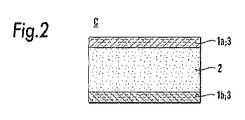
本発明に関連して、図1に示される、データ記憶及びプロセッシング用途のキャパシタ状メモリ回路に用いられるポリマーメモリ材料の疲労及びインプリントの原因の広範な探求が行われた。メモリ回路Cは、この場合には、平行平板キャパシタ状構造の2つの電極の間に挟まれた強誘電体ポリマーである、メモリ材料2と境界をなす第1の電極及び第2の電極1a;1bを備える。電極の間に電圧信号を加えることにより、強誘電体ポリマーは、その分極状態に影響するか、又は呼び掛ける(interrogate)電場を受ける。以下の記述は、有機及びポリマーのエレクトレット及び強誘電体に広く適用できると主張するが、PVDF、並びに、TrFE及び/又はTFEとのそのコポリマー及び/又はターポリマーに重きを置いて、主にポリマー強誘電体を取り扱うであろう。これは、説明に焦点と具体性をもたせ、また関心のある将来の素子に特に関連すると思われる種類の材料を含むようにするためである。
In the context of the present invention, extensive exploration of the causes of fatigue and imprinting of polymer memory materials used in capacitor-like memory circuits for data storage and processing applications as shown in FIG. 1 has been conducted. The memory circuit C, in this case, is a ferroelectric polymer sandwiched between two electrodes of a parallel plate capacitor-like structure, a first electrode and a
実験的及び理論的証拠に基づいて、本発明者等は、疲労及びインプリントの、一般的に繰り返され、普遍的で支配的なメカニズムは、電気的及び化学的ポテンシャルの作用の下での、強誘電体ポリマーの本体内と電極部分近くでの荷電した不純物化学種の再分布であることを見出した。このような不純物は、強誘電体/電極の境界に達すると、強誘電体/電極の境界の深いトラップにより捕捉されるか、あるいは電極材料と反応化学的に反応しうる。不純物は反応生成物を生み出すことがあり、これは、電極に絶縁バリア層と、後に電極に達するイオン性化学種のトラップを形成する。トラップの深さに応じて、局在する電荷が電極表面に蓄積し、脱分極場を作り出して強誘電分域を固定(pinning)することにより、セルの機能を損なう。イオン性又は中性化学種と電極の間の化学反応もまた、電極を物理的に欠陥のあるものにし、それらの伝導率を許容できないレベルに低下させることにより、それらを機能しないものにする。 Based on experimental and theoretical evidence, the inventors have found that the generally repeated and universal dominant mechanism of fatigue and imprint is under the action of electrical and chemical potentials. It was found that this is a redistribution of charged impurity species within the body of the ferroelectric polymer and near the electrode. When such impurities reach the ferroelectric / electrode boundary, they may be trapped by deep traps at the ferroelectric / electrode boundary or may react chemically with the electrode material. Impurities can produce reaction products, which form an insulating barrier layer on the electrode and traps of ionic species that later reach the electrode. Depending on the depth of the trap, localized charge accumulates on the electrode surface, creating a depolarization field and pinning the ferroelectric domain, thereby impairing the function of the cell. The chemical reaction between the ionic or neutral species and the electrode also makes the electrodes physically defective and renders them non-functional by reducing their conductivity to unacceptable levels.
このように、電極又は強誘電体メモリ材料本体の内部境界(すなわち、分域境界、又は無定形領域と結晶領域の間の境界、又は粒界)に欠陥が集積することに伴う2次的な効果により、強誘電体の活性は失われる。これらの欠陥(例えば、イオン化学種)は、合成又は膜製造工程により、強誘電体材料に外からの不純物として前もって存在するか、あるいは、メモリセルの製造中に発生する様々な形態の応力、又は、素子の動作に関連する後の電気的もしくは機械的応力による誘電体の劣化により誘導されるかのいずれかでありうる。 In this way, secondary defects associated with the accumulation of defects at the inner boundaries of the electrode or ferroelectric memory material body (ie, the domain boundaries, or the boundaries between the amorphous and crystalline regions, or the grain boundaries). Due to the effect, the ferroelectric activity is lost. These defects (eg, ionic species) are pre-existing as external impurities in the ferroelectric material by synthesis or film manufacturing processes, or various forms of stress that occur during the manufacture of memory cells, Or it can be induced by degradation of the dielectric due to subsequent electrical or mechanical stress associated with the operation of the device.
前記の有害な現象に対して有効であることが見出され、下に記載され例示される本発明を構成する改善法は、揮発性成分、例えばPZTでの酸素が強誘電体のスイッチング中に失われる、前記の「無機」強誘電体メモリ膜のために発展した改善法とは根本的に異なる。これらの場合には、改善法は、酸素のような失われた化学種を復位させることにより、また、強誘電体本体のドーピング又は化学量論的な比の調節によって空格子点の発生を抑制することにより、空格子点を埋めることに焦点を合わせている。 An improved method of constructing the present invention, found to be effective against the detrimental phenomena described above and illustrated below, is that oxygen in volatile components, such as PZT, is present during ferroelectric switching. It is fundamentally different from the improved method developed for the aforementioned “inorganic” ferroelectric memory films. In these cases, the improved method suppresses the generation of vacancies by relocating lost species such as oxygen and by adjusting the ferroelectric body doping or stoichiometric ratio. By doing so, we focus on filling the vacancies.
本発明の実施形態によれば、強誘電体に接触する電極は、電極/強誘電体メモリ材料の界面に到着する、例えばイオンを捕捉し、電極材料の電気伝導率の低下なしに前記イオンを電極構造に組み入れるように作製される。このことは、電極材料の注意深い選択により実現され、各電極は単一のモノリシックシート又は薄膜であってもよく、あるいは各電極は2つ以上の機能層を含むサンドイッチ構造として作り出される。全電極構造の望ましい機能は、下に列挙されるようなものである。すなわち、
i.電気導電性
ii.有害なイオン性化学種のトラップ/組入れ
iii.強誘電体から電極に向かって移動する不純物が電極に侵入することに対するバリア活性
iv.荷電又は中性化学種が電極から強誘電体に移動することに対するバリア活性
According to an embodiment of the present invention, the electrode in contact with the ferroelectric material arrives at the electrode / ferroelectric memory material interface, for example, traps ions and causes the ions to flow without a decrease in the electrical conductivity of the electrode material. Made to be incorporated into the electrode structure. This is achieved by careful selection of electrode materials, each electrode may be a single monolithic sheet or thin film, or each electrode is created as a sandwich structure comprising two or more functional layers. The desired function of the overall electrode structure is as listed below. That is,
i. Electrical conductivity ii. Trap / incorporation of harmful ionic species iii. Barrier activity against intrusion of impurities moving from ferroelectric to electrode iv. Barrier activity against the migration of charged or neutral species from electrodes to ferroelectrics
ここで、電気導電性により、強誘電体メモリ材料本体から電極に達するイオン性化学種が確実に中和される。こうして、強い局所的分域固定場、又は強誘電体本体にかなりの脱分極場を作り出すことができると思われる電荷の集積は可能でない。電極構造にイオンを組み入れることにより、中和されたイオンは確実に、電極/強誘電体の界面に集積しなくなり、そうしなければ、これは非導電性バリア層を作り出し、構造の破壊さえ引き起こしうるであろう。最後に、優れたバリア性は、裏打ち電極材料又はメモリ素子の他の構成成分を化学的に攻撃するかもしれない、強誘電体本体からの化学的に攻撃的な不純物、あるいは、素子の部分の構造転移により損傷をやはり引き起こしうるであろう、より攻撃性の劣る不純物(例えば、発生ガスにより及ぼされる圧力)の侵入に対する防御を与える。 Here, the ionic species that reach the electrode from the ferroelectric memory material body are reliably neutralized by the electrical conductivity. Thus, it is not possible to build up a strong local domain fixed field, or charge accumulation that could create a significant depolarization field in the ferroelectric body. Incorporating ions into the electrode structure ensures that the neutralized ions do not accumulate at the electrode / ferroelectric interface, otherwise this creates a non-conductive barrier layer and even causes the structure to break. It will be possible. Finally, the excellent barrier properties are those of chemically aggressive impurities from the ferroelectric body, which may chemically attack the backing electrode material or other components of the memory element, or of the part of the element. It provides protection against entry of less aggressive impurities (eg, pressure exerted by the evolved gas) that could still cause damage due to structural transitions.
図2は、本発明によるメモリ回路の第1の好ましい実施形態を示しており、単一の電極材料により、電極1a、1bは最も重要な機能を全て備えている。この場合、電極材料に一様に機能材料が分布していると考えることができる。別法として、機能材料3を、電極1a;1bの電極材料の一部分に含ませることができる。この際は、この部分は、意図された効果をもつために、電極1a;1bの表面に広がり、メモリセルの強誘電体メモリ材料2に接触していなければならない。この場合、2種以上の材料を、この部分の個々の層に含ませる、すなわち、電極材料の層状化された配置に含ませることができる。前記より、第1の実施形態では、本来の電極材料に機能材料を組み入れることにより、図3及び4にそれぞれ示される第2の実施形態の場合のように、機能材料の別個の中間層を用いる必要が無いことが理解されるであろう。第1の実施形態で、機能材料3を組み入れる電極1a、1bを実際に得ることは、次に記載される第2の実施形態の場合より困難な加工上の問題を伴うであろう。しかし、本発明によるメモリ回路の様々な材料及び層を得るための加工上の要件は、後で、簡単に、さらに検討されるであろう。明らかに、この第1の実施形態では、特別な性質の電極材料が必要とされるが、後に実例が示されるように、このような材料は存在する。
FIG. 2 shows a first preferred embodiment of a memory circuit according to the present invention, where the
図3は、本発明の第2の好ましい実施形態によるメモリ回路を示している。それはキャパシタ状構造をしており、電極1a、1bの様々な望ましい機能が、機能材料3の2つの別の中間層3a;3bにより取り入れられている。これらの中間層3a;3bは、電極1a;1bとメモリ材料2の間に挟まれている。中間層3a;3bは、電気導電性であり、またメモリセルCの強誘電体材料2から電極1a;1bに移動するイオン性化学種を、電気伝導率を低下させることなく、その構造に組み入れることができる機能材料3を含む。高導電性電極材料が、電極1a;1bを形成し、外部の駆動及びセンシング回路への優れた電気接続を提供する。電極1a;1bは、強誘電体メモリ材料2に面する側を、中間層3a;3bを形成する導電性イオントラップ機能材料3でコートされている。イオントラップ層3a;3bは、イオン性化学種に対して優れたバリア性を示すので、侵入、並びに、裏打ち電極材料及び可能性としてメモリ回路Cの他の構成成分への化学的攻撃が阻止される。異なる中間層へのこの機能分離を一層多くの層を含む構造に適用して、使用しうる電極材料の範囲を広げ、性能及び/又は生産性を上げることができる。例えば、中間層3a;3bをそれぞれ、いくつかの副層により構成し、副層の各々に特定の機能材料を含ませて、それらを上記のii)〜iv)として列挙されたものの1つのような、特殊な機能に合わせて作り上げることができる。
FIG. 3 shows a memory circuit according to a second preferred embodiment of the present invention. It has a capacitor-like structure, and the various desired functions of the
本発明によるメモリ回路の第2の好ましい実施形態の変形形態が図4に示されており、メモリセルCの各側の、2つの別の中間層3a;4a及び3b;4bの使用が描かれている。強誘電体メモリ材料2に面する中間層3a;3bは、電気導電性であり、強誘電体メモリ材料2からの不純物を吸収する能力がある。中間層4a;4bは同様に、導電性であり、また、高導電性材料、例えば、素子の回路の他の部分に接続される金属である電極層1a、1bへ不純物が通過して移動するのを防ぐ優れたバリア性をもつ機能材料3を含む。高導電性材料は、製造工程を簡単にするために、同じ素子の他の部分に用いられる導体材料であると有利であろう。
A variant of the second preferred embodiment of the memory circuit according to the invention is shown in FIG. 4, depicting the use of two separate
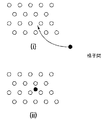
機能材料の動作原理をここでいくらか詳細に説明する。図5a、5b及び5cに概略的に示されるように、いくつかの仕方で、イオン性及び中性不純物化学種を電極構造に組み入れることができる。図5a(i)及び5a(ii)に示されるように、置換は、不純物が機能材料の本来の構成成分を追い出し、その場所を占めることを意味する。外れた本来の構成成分は、今度は別のサイトに移動し、そこでそれは、例えば、この図又は後の図5a、5bのどれかに描かれるメカニズムのいずれかにより、新たに結びつく。図5b(i)及び図5b(ii)は、空格子点を埋めることによる組入れを、また図5c(i)及び図5c(ii)は格子間配置を示している。これらの全ての場合に、機能材料の原子又は空格子点に、ある移動性があることに注意すべきである。したがって、バリア性に優れた密な材料であっても、原子及び分子の再配列により、深く、すなわち強誘電体メモリ材料2と対向する境界の最初のモノレイヤを超えて、不純物を受け入れることができる。
The operating principle of the functional material will now be described in some detail. As shown schematically in FIGS. 5a, 5b and 5c, ionic and neutral impurity species can be incorporated into the electrode structure in several ways. As shown in FIGS. 5a (i) and 5a (ii), substitution means that the impurities expel and occupy the original components of the functional material. The missing original component now moves to another site where it is newly connected, for example, by either the mechanism depicted in this figure or any of the subsequent Figures 5a, 5b. 5b (i) and FIG. 5b (ii) show the incorporation by filling the vacancies, and FIGS. 5c (i) and 5c (ii) show the interstitial arrangement. It should be noted that in all these cases there is some mobility in the atoms or vacancies of the functional material. Therefore, even a dense material having excellent barrier properties can accept impurities deeply, that is, beyond the first monolayer at the boundary facing the
前記の方策により暗に、機能材料3を含む電極1a、1bを有するか、又は別法として機能材料3の中間層3a、3bを有するかのいずれかである、強誘電体メモリ材料2のメモリセルを得る許容される製造方法、並びに、そのような素子を作り出すために選ばれうる材料及び方法の範囲が限定される。したがって、様々な層又は材料界面で、不純物あるいは化学的又は物理的欠陥の発生率が高い粗雑な洗浄及びコーティング方法は避けなければならない。
The memory of the
電極がその望ましい性質を失い始めるまでに、電極構造に組入れられうる不純物の量には、明らかに、ある限度があるにちがいない。しかし、素子寿命の延長は、必ずしも永久に故障しないというわけではなくても、多くの場合、求められていることである。また、多くの事例で、主な問題は、材料合成又は素子製造工程に由来する初期の不純物の集団によるものでありうる。この集団は、電極、又は別の中間層のいずれかに集められ受け入れられると、問題であることを止め、その後長期間、素子の安定した動作が可能になる。 Obviously there must be some limit to the amount of impurities that can be incorporated into the electrode structure before the electrode begins to lose its desirable properties. However, extending the life of the element is often required even if it does not necessarily fail. Also, in many cases, the main problem may be due to an initial population of impurities derived from material synthesis or device manufacturing processes. When this population is collected and accepted at either the electrode or another intermediate layer, it ceases to be a problem and then allows stable operation of the device for a long period of time.
有利には、1種の機能材料又は複数の材料は、電極材料のものと適合性がある電気及び/又は化学的性質をもつべきであり、またこのことは、機能材料が電極材料内に分散しているか、あるいはその表面層として備わるかどうかに関わらず、当てはまる。この意味する所は特に、機能材料は、電極材料と強誘電体又はエレクトレットメモリ材料の双方に対して、化学的に適合しているであろうということである。このことはまた、機能材料は、本来の電極材料又はメモリ材料のいずれかから移動する原子又は分子化学種を組み入れた後、依然として、その元々の電気的及び化学的性質を保持し、また特に、電極材料及びメモリ材料の双方に、いずれの点でも、適合性があるようでなければならないことも意味する。用いられる1種の機能材料又は複数の機能材料は、電極材料に分散させて、また特にその表面層として備えられる場合でも、あるいは電極とメモリ材料の間の中間層として備えられる場合でも、メモリ材料と電極材料の間の電気的減衰を避けるために、メモリ材料のそれに等しいか、より大きい高周波比誘電率をもつべきであるということも、一般に必要とされるであろう。導電性であるが、機能材料の比誘電率は、電極材料のそれよりかなり小さいということがありうるであろうが、好ましくは、強誘電体メモリ材料より大きく、この性質は、移動する原子又は分子化学種が組み入れられてもそのままであるべきである。この種の組入れで、機能材料の伝導率もまた変わるべきではない。 Advantageously, the functional material or materials should have electrical and / or chemical properties that are compatible with those of the electrode material, which means that the functional material is dispersed within the electrode material. This is true regardless of whether or not it is provided as a surface layer. This means in particular that the functional material will be chemically compatible with both the electrode material and the ferroelectric or electret memory material. This also means that the functional material still retains its original electrical and chemical properties after incorporating atomic or molecular species that migrate from either the original electrode material or memory material, and in particular It also means that both the electrode material and the memory material must be compatible in any respect. The functional material or functional materials used may be dispersed in the electrode material and in particular if it is provided as its surface layer or as an intermediate layer between the electrode and the memory material. It would also generally be necessary to have a high-frequency dielectric constant equal to or greater than that of the memory material to avoid electrical attenuation between the electrode material and the electrode material. Although it may be conductive, the dielectric constant of the functional material may be significantly less than that of the electrode material, but is preferably larger than the ferroelectric memory material, this property being a moving atom or It should remain intact even if molecular species are incorporated. With this type of incorporation, the conductivity of the functional material should also not change.
本発明によるメモリ回路を、このようなメモリ回路の、マトリックス−アドレス指定可能アレイのメモリ回路として用いることができるであろう。別の言い方をすると、それらは、図6aの平面図と、図6bにX−Xラインに沿う横断面で示される受動マトリックス−アドレス指定可能メモリ素子を構成するであろう。メモリ素子は、アドレス指定動作で、メモリセルCをオン、オフに切り替える、メモリ回路に接続するスイッチングトランジスタがないので、受動マトリックス素子と名づけられる。これは、メモリセルCのメモリ材料は、それがアドレス指定されていない状態では、マトリックス−アドレス指定可能素子のアドレス指定電極のどれとも接触していないことを意味するであろう。基本的に、この種のメモリ素子は、第1の組の平行ストリップ状電極1bをもち、図6bでは、これは基板上に位置し、機能材料の中間層3bにより覆われ、強誘電体メモリ材料、すなわち強誘電体ポリマー2の大域層がこれに続くように示されており、今度はそれが機能材料の大域層3aにより覆われ、その上に、同様の平行ストリップ状電極1aを備えるが、直交する電極マトリックスを形成するように、電極1bに直角に配向する別の電極の組を備える。電極1aを、例えば、マトリックス−アドレス指定可能メモリ素子のワード線と見なすことができ、電極1bをそのビット線と見なすことができる。ワード線1aとビット線1bの間の重なりで、メモリセルは、メモリ材料2の大域層にマトリックスとして画定される。このように、メモリ素子は、マトリックスの電極の重なりの数に対応する複数のメモリ回路Cを備える。メモリ回路Cは、図6cの横断面により詳細に示されており、本発明によるメモリ回路の第2の好ましい実施形態に対応する。別の言い方をすると、機能材料3は、それぞれ電極1a及び1bと境界をなし、それらの間にメモリ材料2を挟む個々の中間層3a、3bに含まれる。図6a及び6bに示される類のメモリ素子では、電極1a上に絶縁層(あるいは、いわゆる分離層)を備えることができ、次に第2の同様の素子をその上部に積み重ね、それを続けて、先行技術において知られている多層又は立体的メモリ素子を形成できることが理解されるであろう。図6aのメモリ素子でそれぞれワード及びビット線となる電極1a及び1bは全て、図には周辺の外部回路構成が示されていないが、マトリックス−アドレス指定可能メモリ素子のメモリセルへの書込み/読込み動作を実施する適当な駆動及び制御及びセンシング回路に接続されるであろうということが理解されるべきである。
The memory circuit according to the invention could be used as a memory circuit of a matrix-addressable array of such a memory circuit. In other words, they would constitute a passive matrix-addressable memory element shown in plan view in FIG. 6a and in cross section along line XX in FIG. 6b. The memory element is named a passive matrix element because there is no switching transistor connected to the memory circuit that switches the memory cell C on and off in an addressing operation. This would mean that the memory material of memory cell C is not in contact with any of the addressing electrodes of the matrix-addressable element when it is not addressed. Basically, this type of memory element has a first set of
この種のマトリックス−アドレス指定可能メモリ素子に機能材料を備えるには、製造の詳細に対する、いくらかの注意が必要とされる。例えば、ビット線電極1bを基板S上に配置し、最初に、その基板を覆う大域層として堆積させることができ、その後、例えば標準的なフォトリソグラフィ法で、ストリップ状ビット線電極1bが形成されるように、電極はパターン化される。別法として、電極1bに対応する横断面をもつ平行な凹みを基板に形成し、次に、適当な処理をした電極材料で充填し、必要であれば、電極の上部表面が基板のそれと同一平面になるまで平坦化することができるであろう。機能材料3が電極材料に組み入れられる場合、物理又は化学気相堆積を用いて、電極材料に機能材料が同時に又は徐々に組み入れられるように両材料を堆積させることができる。別法として、後の別のステップにおいて、層3b又は機能材料のいずれかをメモリ素子の大域層として付着させることができ、次に、メモリ材料の大域層2を堆積し、その後、メモリ材料2の大域層を覆う、機能材料の別の大域層3aが備えられる。最後に、図6aに示されるように、ワード線電極1aが備えられ、そして、可能性として、絶縁及び分離機能がある平坦化層により覆われる。得られる構造は、言うまでもなく、受動マトリックス−アドレス指定可能メモリアレイに、本発明による複数のメモリ回路Cを集積するメモリ素子である。機能材料3が個々の中間層3a、3bに含まれる場合、これらの層の双方、並びにメモリ材料2は大域層、すなわちメモリ素子の、パターン化されていない層として備えられるので、単一のメモリ回路を、その数が、数千万又は数億、あるいは一層多くに達し、それぞれ別々のメモリ回路の予め決められた分極状態又は値として、それと同数のビットを記憶する容量をもつ、このようなメモリ回路のアレイへと集積化することができる。さらに、この種のメモリマトリックス−アドレス指定可能メモリ素子は、書込み及び読込みのための外部回路構成の適当な配置により、読込みの書込み動作を、非常に大規模な並列方式で実施することができる。
Providing functional materials in this type of matrix-addressable memory element requires some attention to manufacturing details. For example, the
本発明によるメモリ回路で使用されうる機能材料の様々な例が、フッ素含有メモリ材料と共に使用するのに適する機能材料又はその中間層を明確に記載して、これから与えられるであろう。この重要視は、特定のフッ素含有ポリマー強誘電体、特にPVDF、並びにVDFとTrFEのコポリマーは、将来のデータ記憶素子のメモリ材料として特に有望視されているという事実に基づいている。それはまた、フッ素含有メモリ材料は、中性、並びにイオンの形態のフッ素及びフッ化水素の移動性と化学的攻撃性により、例外的な難題を提起するという事実でもある。 Various examples of functional materials that can be used in the memory circuit according to the present invention will now be given, with a clear description of functional materials or intermediate layers suitable for use with fluorine-containing memory materials. This emphasis is based on the fact that certain fluorine-containing polymer ferroelectrics, especially PVDF, and copolymers of VDF and TrFE are particularly promising as memory materials for future data storage elements. It is also the fact that fluorine-containing memory materials pose exceptional challenges due to the neutrality and mobility and chemical aggressiveness of fluorine and hydrogen fluoride in the ionic form.
ダイヤモンド様ナノコンポジット(DLN)膜をもつ電極
最近、新しいタイプの膜が開発され、非常に優れた耐腐食性とバリア性を、膜成長の間に組成を変えることにより18桁の大きさに渡って調節できる電気導電性と共に併せもっている(比較、例えば、「ダイヤモンド様ナノコンポジット又はドープされたダイヤモンド様ナノコンポジット膜の形成方法(Method for forming Diamond−Like Nanocomposite or Doped−Diamond−Like Nanocomposite Filems)」、米国特許第5,352,493号(1994年);(Veniamin DorfmanとBoris Pypkin))。ダイヤモンド様ナノコンポジット(DLN)カーボン膜と名づけられているので、これらの膜は、一層よく知られたダイヤモンド様カーボン(DLC)膜にいくらか似ているが(比較、例えば、「真空でのダイヤモンド様カーボンコーティング形成方法(Method of forming Diamond−Like Carbon Coating in Vacuum)」、公開国際出願WO98/54376(A.I.Maslov他))、水素で安定化され、主にダイヤモンド結合した炭素の相互貫入ランダムネットワーク、及び、酸素で安定化されたガラス状ケイ素からなる。このC−Si自己安定化アモルファス構造は、比抵抗を10e−4Ωcmまで下げる、第3の相互貫入ネットワークを形成する金属を導入するマトリックスを形成する。望みの性質に応じて、Li、Ag、Cu、Al、Zn、Mg、Nb、Ta、Cr、Mo、W、Rh、Fe、Co、及びNiを含めて、広い範囲から金属を選択することができる。ほとんどどんな基板材料上にも、基板を単に穏やかに温度上昇させて(室温堆積温度)、これらの膜を高速で堆積させることができる。接着性は、本発明の状況に関連する実質的に全ての材料、すなわち、電極及び強誘電体として使用される、無機、並びに有機及びポリマー材料(例えば、金属、酸化物、セラミック、プラスチック)に対して優れている。テフロン(登録商標)で観察された優れた接着性は、PVDF、並びにTrFEとのそのコポリマーのような、化学的に密接に関連するポリマー強誘電体との関連で、実際的な意味がある。
Electrodes with diamond-like nanocomposite (DLN) films Recently, a new type of film has been developed, which provides exceptional corrosion resistance and barrier properties over 18 orders of magnitude by changing the composition during film growth. (For example, “Method for forming Diamond-Like Nanocomposite or Doped-Diamond-Like Nanocomposite”). U.S. Pat. No. 5,352,493 (1994); (Veniamin Dorfman and Boris Pypkin)). Named diamond-like nanocomposite (DLN) carbon films, these films are somewhat similar to the more well-known diamond-like carbon (DLC) films (for example, “Diamond-like in vacuum” Carbon coating forming method (Method of forming Diamond-Like Carbon Coating in Vacuum), published international application WO 98/54376 (AI Maslov et al.), Hydrogen-stabilized, mainly diamond-bonded carbon interpenetrating random It consists of a network and glassy silicon stabilized with oxygen. This C-Si self-stabilizing amorphous structure forms a matrix that introduces a metal that forms a third interpenetrating network that lowers the resistivity to 10e-4 Ωcm. Depending on the desired properties, metals can be selected from a wide range including Li, Ag, Cu, Al, Zn, Mg, Nb, Ta, Cr, Mo, W, Rh, Fe, Co, and Ni. it can. On almost any substrate material, these films can be deposited at high speeds by simply warming the substrate gently (room temperature deposition temperature). Adhesiveness is applicable to virtually all materials relevant to the context of the present invention, ie inorganic, organic and polymeric materials (eg metals, oxides, ceramics, plastics) used as electrodes and ferroelectrics. It is superior to it. The superior adhesion observed with Teflon has practical implications in the context of PVDF and chemically closely related polymer ferroelectrics such as its copolymer with TrFE.
DLN膜の重要な特徴は、微細構造特性、並びに化学的性質を、それぞれの所定の用途に合わせられることである。例として、強誘電体から、DLNからなる電極表面に移動する攻撃的化学種を組み入れるという問題を考える。前記の参照文献に記載されているように、DLNは、相互貫入サブネットワークのウェブ(web)を含む。電極構造の様々な要件、すなわち、構造に欠陥がないこと、バリア性、電気伝導率、及び強誘電体メモリ材料からの不純物の受け入れ、を満たすように、これらのサブネットワークを選ぶことができる。 An important feature of DLN films is that the microstructural properties as well as the chemical properties can be tailored for each given application. As an example, consider the problem of incorporating an aggressive species that migrates from a ferroelectric to an electrode surface made of DLN. As described in the aforementioned references, the DLN includes a web of interpenetrating sub-networks. These sub-networks can be chosen to meet the various requirements of the electrode structure, i.e., that the structure is defect free, barrier properties, electrical conductivity, and acceptance of impurities from the ferroelectric memory material.
具体的に、図7に示されるDLN膜の構造を考える。1つのネットワークは水素により安定化された、主にsp3結合炭素からなり、構造の骨格を構成する。別のネットワークは、酸素により安定化されたケイ素からなり、C−Hのネットワークと絡み合い、C−Hのネットワークと共に、電極構造全体に機械的強度とバリア性を付与する。第3に、ドーパント元素、又は周期律表の1〜7b及び8族から選択された元素を含むドーパント化合物のネットワークがある。これらのドーパントは、他の2つのネットワークの中間に形成されたナノポアのネットワークに受け入れられており、この場合、パーコレーション臨界値を超える濃度の金属であり、電気導電性を付与し、全ネットワーク構造のバリア性に寄与している。DLN製造過程の間に、制御された仕方で、他のドーパントもまた組み入れることができる。また、膜の厚さ内にドーパントの濃度勾配を作り出すことができる。ここで、処理されようとしている不純物が、PVDF及びP(VDF−TrFE)強誘電体との関連で実際に意味があると思われる、例えば、F−イオンとフッ化水素であると仮定する。DLN膜により覆われる電極境界に達すると、不純物はナノポアネットワークに入り、そこで動けなくなるであろう。ネットワーク内部へのトラップは、図5a〜cに示される一般的メカニズムのいずれかにより起こるであろう。物理と化学に熟達した人には明らかであるように、図7の構造は、好ましいトラップメカニズムを選択する異例の範囲の好機を提供している。通常、深いトラップが、永久的な不動化にとって望ましい。これを実現する1つの方法は、不純物化学種、例えばフッ素と強い化学反応性を示し、反応生成物が電極の機能に有害な影響を与えることなくその構造に閉じ込められたままになるサイトを、電極材料内部に備えることである。ここの例では、ナノポアネットワーク内のドーパントだけでなく、酸素で安定化されたケイ素のネットワーク自体も、電極構造の犠牲反応化学種として役立ちうることに気づく。例えば、HF酸は、DLNのSi−Oネットワークを選択的にエッチングすることが知られている(比較、V.Dorfman、「ダイヤモンド様ナノコンポジット(DLN)(Diamond−like nanocomposites(DLN))」、Thin Solid Films 212 267−273(1992))。 Specifically, consider the structure of the DLN film shown in FIG. One network consists mainly of sp 3 bonded carbon stabilized by hydrogen and constitutes the framework of the structure. Another network is made of silicon stabilized by oxygen, and is intertwined with the C—H network, and together with the C—H network, provides mechanical strength and barrier properties to the entire electrode structure. Thirdly, there is a network of dopant compounds containing dopant elements or elements selected from groups 1-7b and group 8 of the periodic table. These dopants are accepted by the nanopore network formed in the middle of the other two networks, in this case a concentration of metal above the percolation critical value, which imparts electrical conductivity and contributes to the overall network structure. Contributes to barrier properties. Other dopants can also be incorporated in a controlled manner during the DLN manufacturing process. It is also possible to create a dopant concentration gradient within the thickness of the film. It assumed to be hydrogen fluoride ions - Here, an impurity that is about to be processed, actually mean in the context of PVDF and P (VDF-TrFE) ferroelectrics thought to, for example, F. When the electrode boundary covered by the DLN film is reached, the impurities will enter the nanopore network where they will be unable to move. Traps inside the network will occur by any of the general mechanisms shown in FIGS. As will be apparent to those skilled in physics and chemistry, the structure of FIG. 7 provides an unusual range of opportunities for selecting a preferred trapping mechanism. Usually deep traps are desirable for permanent immobilization. One way to achieve this is to create sites that are highly chemically reactive with impurity species, such as fluorine, and the reaction products remain trapped in the structure without adversely affecting the function of the electrode, It is to be provided inside the electrode material. In this example, we notice that not only the dopant in the nanopore network, but also the oxygen stabilized silicon network itself can serve as a sacrificial species for the electrode structure. For example, HF acid is known to selectively etch the Si-O network of DLN (Comparison, V. Dorfman, “Diamond-like nanocomposites (DLN))”, Thin Solid Films 212 267-273 (1992)).
機能材料としての導電性炭化物
遷移金属の炭化物は融点が高く、耐摩耗性に優れ、化学的に安定である。多くの遷移金属窒化物はまた優れた導体である。ここでは、炭化タンタル(TaC)、炭化チタン(TiC)、炭化ジルコニウム(ZrC)及び炭化ハフニウム(HfC)を特に挙げておく。特にTiCは、現在のTi電極と組み合わせると興味深い。これらの化合物は、NaCl構造をなし、金属結合、共有結合及び少量のイオン性結合が複雑に組み合わさっている。比抵抗は結晶の完全性に依存し、通常30〜50・10−8Ωmである。
Conductive carbides as functional materials Transition metal carbides have a high melting point, excellent wear resistance, and are chemically stable. Many transition metal nitrides are also excellent conductors. Here, tantalum carbide (TaC), titanium carbide (TiC), zirconium carbide (ZrC), and hafnium carbide (HfC) are specifically mentioned. TiC is particularly interesting when combined with current Ti electrodes. These compounds have a NaCl structure and are a complex combination of metal bonds, covalent bonds and small amounts of ionic bonds. The specific resistance depends on the completeness of the crystal and is usually 30-50 · 10 −8 Ωm.
この材料の薄膜は通常、グロー放電法、例えば、反応性マグネトロンスパッタリングを用いて形成される。品質の良い膜を生成させる方法は、十分に発達しており、この材料は、例えば、拡散バリア、耐摩耗性コーティング、及び光学的コーティングとして用いられている。 A thin film of this material is usually formed using a glow discharge method, such as reactive magnetron sputtering. Methods for producing quality films are well developed and this material is used, for example, as a diffusion barrier, abrasion resistant coating, and optical coating.
機能材料としての導電性酸化物
これには、ドープ/無ドープの2元系又は3元系酸化物が含まれる。通常の堆積法は、CVD/スピン(Sn2O3:In、SnO2:F、ZnO:Al)、及びスパッタリング(LSMO、RuO、IrO2、ITO)である。
Conductive oxides as functional materials This includes doped / undoped binary or ternary oxides. Common deposition methods are CVD / spin (Sn 2 O 3 : In, SnO 2 : F, ZnO: Al), and sputtering (LSMO, RuO, IrO 2 , ITO).
機能材料としての導電性ホウ化物
これには、HfB、ZrB、CrBが含まれる。
Conductive borides as functional materials This includes HfB, ZrB, CrB.
機能材料としての導電性窒化物
窒化物化合物の伝導率は広い範囲に渡り、その材料を金属、半導電性又は絶縁性にする。特に、遷移金属窒化物は、大きな科学的関心を集めてきた。これらの材料は高融点であり、優れた耐磨耗性を示し、また化学的に安定である。多くの遷移金属窒化物はまた優れた導体である。ここでは、4A族の窒化物である、窒化チタン(TiN)、窒化ジルコニウム(ZrN)及び窒化ハフニウム(HfN)を特に挙げておく。特にTiNは、Ti電極と組み合わせると興味深い。これらの化合物は、NaCl構造をなし、金属結合、共有結合及びイオン性結合が複雑に組み合わさっている。比抵抗は結晶の完全性に依存し、通常20〜30・10−8Ωmである。この種の薄膜は通常、グロー放電法、例えば、反応性マグネトロンスパッタリングを用いて形成される。品質の良い膜を生成させる方法は、十分に発達しており、この材料は、例えば、拡散バリア、耐摩耗性コーティング、及び光学的コーティングとして用いられている。さらに、TaN、VN、NbNのような5A族の窒化物、及びCrNのような6A族の窒化物を用いることができる。
Conductive nitrides as functional materials Nitride compounds have a wide range of conductivity, making them metallic, semi-conductive or insulating. In particular, transition metal nitrides have attracted great scientific interest. These materials have a high melting point, exhibit excellent wear resistance, and are chemically stable. Many transition metal nitrides are also excellent conductors. Here, titanium nitride (TiN), zirconium nitride (ZrN), and hafnium nitride (HfN), which are Group 4A nitrides, are specifically mentioned. TiN is particularly interesting when combined with a Ti electrode. These compounds have a NaCl structure and are a complex combination of metal, covalent and ionic bonds. The specific resistance depends on the completeness of the crystal and is usually 20 to 30 · 10 −8 Ωm. This type of thin film is typically formed using a glow discharge method, such as reactive magnetron sputtering. Methods for producing quality films are well developed and this material is used, for example, as a diffusion barrier, abrasion resistant coating, and optical coating. Further, a Group 5A nitride such as TaN, VN, and NbN, and a Group 6A nitride such as CrN can be used.
関連する文献として、例えば、Louis E.Tothによる「遷移金属炭化物及び窒化物(Transition metal carbide and nitrides)」(Academic Press 1971)の、J.E.Greene、J.E.Sundgren、L.G.Hultman等の論文を参照。 As related literature, for example, Louis E. et al. Toth, “Transition metal carbides and nitrides” (Academic Press 1971), J. Org. E. Greene, J. et al. E. Sundren, L.M. G. See Hultman et al.
機能材料としての導電性ポリマー
最初の高導電性ポリマーは、銀色の全トランスポリアセチレン(PA)(H.Shirakawa)、後には、例えばI2を用いる同じ材料のドーピング(H.Shirakawa,E.J.Louis,A.G.MacDiarmid,C.K.Chiang and A.J.Heeger;J.Chem.Soc.Chem.Comm.(1977)579)が開発され、約25年前に合成された。これらの膜の伝導率は、103(Ωcm)−1の程度であることが見出された。間もなく、ポリ(p−フェニレン)(PPP)、ポリピロール(PPy)、ポリ(p−フェニレンビニレン)(PPV)、ポリチオフェン(PT)及びポリアニリン(PANI)のような他の共役ポリマーにドープすることが可能であることも発見された。しかし、これらの材料の欠点は、それらが加工できないことであった。
Conductive polymer as a functional material The first highly conductive polymer is silver all-trans polyacetylene (PA) (H. Shirawa), later doping of the same material using eg I 2 (H. Shirawa, EJ Louis, AG MacDiarmid, C. K. Chiang and A. J. Heeger; J. Chem. Soc. Chem. Comm. (1977) 579) were developed and synthesized about 25 years ago. The conductivity of these films was found to be on the order of 10 3 (Ωcm) −1 . Soon, other conjugated polymers such as poly (p-phenylene) (PPP), polypyrrole (PPy), poly (p-phenylene vinylene) (PPV), polythiophene (PT) and polyaniline (PANI) can be doped. It was also discovered. However, a drawback of these materials is that they cannot be processed.
80年代の中頃に、ポリチオフェンにアルカリ側鎖を付けて、ポリ(3−アルキルチオフェン)(P3AT)にすると、共役ポリマーが加工可能(可溶性でも溶融可能でもある)であることが示された。これらの材料にドープする可能性もまた示されたが(Sato,Tanaka、Kaeriyama;Synthetic Metals 18(1987)229)、安定性に乏しかった(G.Gustafsson,O.Inganas,J.O.Nilsson,B.Liedberg,Synthetic Metals 31(1988)297)。 In the mid 80's, polythiophene (P3AT) with an alkali side chain was shown to be processable (both soluble and meltable) when poly (3-alkylthiophene) (P3AT). The possibility of doping these materials was also shown (Sato, Tanaka, Kaeriyama; Synthetic Metals 18 (1987) 229), but was less stable (G. Gustafsson, O. Inganas, J. O. Nilsson, B. Liedberg, Synthetic Metals 31 (1988) 297).
後年、導電性ポリマーはさらに進歩し、ドープされた状態においても、加工可能で(例えば、ポリアニリンドデシルベンゼンスルホン酸、Pani DBSA)、また可溶性の(例えば、ポリスチレンスルホン酸を含むポリ(エチレンジオキシチオフェン)、PEDOT−PSS)材料が得られた。今日、102(?)から105(Ωcm)−1の範囲の伝導率をもつ導電性ポリマーが多くの用途向けに商品化されている。 In later years, conductive polymers have further advanced and can be processed even in the doped state (eg, polyaniline dodecylbenzene sulfonic acid, Pani DBSA) and soluble (eg, poly (ethylenedioxy containing polystyrene sulfonic acid). Thiophene), PEDOT-PSS) material was obtained. Today, conductive polymers with conductivity in the range of 10 2 (?) To 10 5 (Ωcm) −1 are commercialized for many applications.
機能材料としての導電性ケイ化物
これには、TiSi2が含まれる。
This conductive silicide as functional materials include TiSi 2.
他のタイプの機能材料
これらには、グラファイトカーボン、C60(バックミンスターフラーレン)のようなフラーレン、及び官能基としてシアノ(CN)をもつ物質が含まれる。
Other types of functional materials These include graphite carbon, fullerenes such as C60 (Buckminsterfullerene), and materials with cyano (CN) as a functional group.
本発明によるメモリ回路では、メモリセルのメモリ材料は、好ましくは、強誘電体又はエレクトレットメモリ材料である。この材料は、現在最も普及したポリマーであり、また最もよく理解されているポリマーメモリ材料であると現在見なしうる、ポリビニリデン−トリフルオロエチレン(PVDF−TrFE)であると有利でありうる。メモリ材料が、電極の間に介在して、完全なメモリ回路を形成し、通常これらの電極は、好ましくは、アルミニウム、白金、チタン、銅又はこれらのコンポジットの合金からなる金属である。電極材料は如何なる場合でも優れた電気導電性を示すであろう。これに関連して、当分野の技術者によく理解されており、文献で大いに検討されてきた問題は、電極材料より元々ずっと融点が低いポリマーメモリ材料上に直接金属を被覆して電極を付ける必要性である。基本的には、前記の好ましい様々なタイプからなる本発明による機能材料を、本発明のメモリ回路に備えようとする時にも同じ問題が発生する。この問題は、実現されようとする実際のさらなる実施形態により、いくらか異なる仕方で現れる。一般に、第1の電極、例えば1aの電極材料は、例えば、物理又は化学気相堆積により、示されていない基板上に堆積されることにより、メモリ回路に備えられる。この時、図2に示される第1の実施形態では、機能材料もまた同じ気相堆積法に含めて、電極材料に一様に分布した機能材料を含む電極1aを形成することができる。別法として、混合されていない電極材料が、工程の初期段階に、前と同じ物理又は化学気相堆積により堆積され、その後、次の工程段階で、機能材料が量を増やしながら加えられる。この時、1種より多い機能材料の堆積を異なる工程段階で行うことができ、その結果これらの材料は、電極材料の表面に隣接する電極材料の一部分に、層状化するか、もしくは傾斜分布し、次のメモリ材料の堆積は、スピン又はディップコーティング法により行うことができる。ここで、低融点のメモリ材料は、1種又は複数の機能材料を組み入れた電極材料の固化した層の上に堆積されるので、次の加工ステップには、熱的、又は化学的適合性のいずれの問題も存在しないであろう。しかし、1種又は複数の混合された機能材料を含む第2の電極、例えば1bを、ポリマーメモリ材料に堆積させようとする時には、このさらなる堆積過程が、すでに備わるポリマーメモリ材料に悪影響を及ぼさないように、特別な注意を要する。したがって、ポリマーメモリ材料の表面に最初に電極又は機能材料のいずれかの膜を形成する時は、ポリマー材料への入射熱フラックスが少ない物理又は化学気相堆積が用いられるべきである。例えば、メモリ材料の体積要素に、その融解熱を超える熱エネルギーが蓄積しないように、この段階での、ポリマーメモリ材料への熱エネルギーの入射を、ある特定の値より十分低く保つことができるであろう。
In the memory circuit according to the invention, the memory material of the memory cell is preferably a ferroelectric or electret memory material. This material may advantageously be polyvinylidene-trifluoroethylene (PVDF-TrFE), which is currently the most popular polymer and can now be considered the best understood polymer memory material. A memory material is interposed between the electrodes to form a complete memory circuit, which is usually a metal made of aluminum, platinum, titanium, copper or an alloy of these. The electrode material will in any case exhibit excellent electrical conductivity. In this context, problems well understood by those skilled in the art and have been extensively discussed in the literature are the direct metal coatings on polymer memory materials that have a much lower melting point than the electrode materials. Is a necessity. Basically, the same problem arises when it is intended to provide the memory circuit of the present invention with the functional materials according to the present invention of the various preferred types described above. This problem appears in a somewhat different way depending on the actual further embodiment to be realized. In general, the first electrode, eg 1a electrode material, is provided in a memory circuit by being deposited on a substrate not shown, for example by physical or chemical vapor deposition. At this time, in the first embodiment shown in FIG. 2, the functional material is also included in the same vapor deposition method, and the
機能材料又は電極材料又はこれらの混合体のいずれかの最初の薄膜により、メモリ材料が一旦コートされると、メモリ材料がもはや悪影響を及ぼされないような、すでに付着した薄膜の十分な熱散逸容量を拠り所として、堆積工程を続けることができる。上の工程についての考察は、機能材料が、電極材料に混合されて備えられるか、あるいは、例えば図3に示されるように、電極材料の表面層、又は電極とメモリ材料の間の中間層を形成する別の工程で付けられるかに関わらず、一般に当てはまることに注意すべきである。上の例2又は例5に関連して簡単に記載された手段により、機能材料を堆積させることができることにも注意すべきである。 With the first thin film of either the functional material or the electrode material or a mixture thereof, once the memory material is coated, there is sufficient heat dissipation capacity of the already deposited thin film so that the memory material is no longer adversely affected. As a basis, the deposition process can continue. The discussion of the above process is that the functional material is provided mixed with the electrode material, or the surface layer of the electrode material, or an intermediate layer between the electrode and the memory material, as shown for example in FIG. It should be noted that this is generally true regardless of whether it is applied in a separate process to form. It should also be noted that the functional material can be deposited by means briefly described in connection with Example 2 or Example 5 above.
導電性ポリマーが機能材料として用いられる場合、これを通常の材料、すなわち金属の電極材料と混合することはできないが、如何なる場合でも、金属の表面に堆積して、本発明のメモリ回路の中間層となるであろう。従来技術による応用の紹介において記載したように、導電性ポリマーだけを電極材料として使用する、すなわち、こうして金属の電極を全く無くする試みがなされてきた。しかし、導電性ポリマーは、ポリマーメモリ材料と化学的に異なり、これを防ぐことが本発明の主な目的である、移動性の荷電及び/又は中性粒子がそれらの間を移動することによる、それらの劣化の可能性が依然としてあるであろう。したがって、導電性ポリマー材料だけの電極を用いる場合には、有利には、この種の電極にそのドーパントとして機能材料を組み入れることができ、その結果、この場合、必要とされる導電性と電荷移動機能と、機能材料の望ましい効果、すなわち、電極材料又はメモリ材料のいずれかに含まれ、それらの間を移動する傾向がある原子又は分子化学種を組み入れることとを電極が完全に併せもつ。 If a conductive polymer is used as the functional material, it cannot be mixed with a normal material, i.e. a metal electrode material, but in any case it is deposited on the surface of the metal and the intermediate layer of the memory circuit of the invention. It will be. As described in the introduction of prior art applications, attempts have been made to use only conductive polymers as electrode material, i.e. thus eliminating any metal electrodes. However, conductive polymers are chemically different from polymer memory materials, and it is the main object of the present invention to prevent this, due to mobile charged and / or neutral particles moving between them. There will still be a possibility of their degradation. Thus, when using electrodes of only conductive polymer material, it is advantageous to incorporate functional materials as dopants in this type of electrode, so that in this case the required conductivity and charge transfer are required. The electrode is a perfect combination of function and the desired effect of the functional material, i.e., incorporating atomic or molecular species that are included in and tend to move between the electrode material or the memory material.
最後に、追加の、示されていない基材、又は、例えば適当な電気絶縁性材料のバックプレーン(backplane)の使用を含む第3の工程ステップで、機能材料が組み入れられたか、あるいはその1つ又は複数の表面層としてもつかのいずれかである第2の電極を供用し、その後、貼り付けることができる第2の電極層及び/又は機能材料層を、低温の工程でメモリ材料にラミネートすることにより、耐火性電極材料の通常の金属被覆又は堆積法に含まれる複雑さを避けることも可能であることに注意すべきである。これは特に、機能材料及び(又は)電極をメモリ材料に拡散することが大いに排除し得るという事実を考慮に入れるとまた、特に有利になり得る。 Finally, a functional material has been incorporated, or one of them, in a third process step that includes the use of an additional, not shown substrate or, for example, a backplane of a suitable electrically insulating material. Alternatively, the second electrode, which is either a surface layer or a plurality of surface layers, is used, and then the second electrode layer and / or the functional material layer that can be attached is laminated to the memory material in a low-temperature process. It should be noted that it is possible to avoid the complexity involved in conventional metallization or deposition methods of refractory electrode materials. This can also be particularly advantageous, especially in view of the fact that diffusing functional materials and / or electrodes into the memory material can be largely eliminated.
当分野の技術者に知られているように、それらが電極層、メモリ材料層又は機能材料の中間層であるかどうかに関わらず、メモリ回路の全ての層を、本明細書に記載された堆積法のいずれかにより、薄膜として堆積させることができることが理解されるべきである。このことは当分野の技術者には明らかであろうし、また、例えば、強誘電体ポリマーのような有機材料系の強誘電体メモリは、今日、薄膜としてだけ想定されているので、実際に大きな意味がある。 As known to those skilled in the art, all layers of the memory circuit are described herein, whether they are electrode layers, memory material layers, or functional material intermediate layers. It should be understood that it can be deposited as a thin film by any of the deposition methods. This will be apparent to those skilled in the art, and organic material-based ferroelectric memories, such as ferroelectric polymers, for example, are currently only envisioned as thin films, so they are actually large. There is a meaning.
Claims (24)
前記電極材料又は前記メモリセルの前記メモリ材料(2)のいずれかに含まれ、また、移動性の荷電及び(又は)中性粒子の形態で、前記電極材料から前記メモリ材料(2)へ、あるいは後者から前者へ移動する傾向を示す原子又は分子化学種を、物理的及び(又は)化学的に大量に組み入れることができる、少なくとも1種の機能材料(3)を、前記電極(1a;1b)の少なくとも一方が含むことにより、前記電極材料又は前記メモリセルの前記メモリ材料(2)のいずれかの機能特性への悪影響を打ち消すことができることを特徴とする、前記強誘電体又はエレクトレットメモリ回路(C)。 A ferroelectric or electret memory cell having a memory material (2) exhibiting hysteresis and capable of being polarized into a positive or negative polarization state having a predetermined polarization value, and polarizing an unpolarized memory cell, or By applying an appropriate voltage to these electrodes that causes a potential difference that causes switching between one polarization state of the memory cell and its opposite polarization state, or that causes a temporary change in the polarization state or its value to the memory cell, Ferroelectric, comprising first and second electrodes (1a, 1b) arranged to be able to be generated across the memory material (2) and in direct or indirect contact with the memory material Body or electret memory circuit (C), in particular a ferroelectric or electret memory circuit with improved fatigue resistance,
Contained in either the electrode material or the memory material (2) of the memory cell, and from the electrode material to the memory material (2) in the form of mobile charged and / or neutral particles, Alternatively, at least one functional material (3), capable of physically and / or chemically incorporating large quantities of atomic or molecular species that tend to migrate from the latter to the former, comprises the electrodes (1a; 1b). ), The adverse effect on the functional characteristics of either the electrode material or the memory cell (2) of the memory cell can be canceled out. (C).
Applications Claiming Priority (2)
| Application Number | Priority Date | Filing Date | Title |
|---|---|---|---|
| NO20015735A NO20015735D0 (en) | 2001-11-23 | 2001-11-23 | underlayer |
| PCT/NO2002/000437 WO2003044801A1 (en) | 2001-11-23 | 2002-11-22 | A ferroelectric or electret memory circuit |
Publications (1)
| Publication Number | Publication Date |
|---|---|
| JP2005510078A true JP2005510078A (en) | 2005-04-14 |
Family
ID=19913059
Family Applications (1)
| Application Number | Title | Priority Date | Filing Date |
|---|---|---|---|
| JP2003546352A Pending JP2005510078A (en) | 2001-11-23 | 2002-11-22 | Ferroelectric or electret memory circuit |
Country Status (12)
| Country | Link |
|---|---|
| EP (1) | EP1446806B1 (en) |
| JP (1) | JP2005510078A (en) |
| KR (1) | KR100603670B1 (en) |
| CN (1) | CN100449640C (en) |
| AT (1) | ATE291273T1 (en) |
| AU (1) | AU2002366187B2 (en) |
| CA (1) | CA2464082C (en) |
| DE (1) | DE60203321T2 (en) |
| ES (1) | ES2238638T3 (en) |
| NO (1) | NO20015735D0 (en) |
| RU (1) | RU2269830C1 (en) |
| WO (1) | WO2003044801A1 (en) |
Cited By (5)
| Publication number | Priority date | Publication date | Assignee | Title |
|---|---|---|---|---|
| JP2005083961A (en) * | 2003-09-10 | 2005-03-31 | ▲高▼木 敏行 | Strain sensor |
| JP2007013116A (en) * | 2005-05-31 | 2007-01-18 | Semiconductor Energy Lab Co Ltd | Semiconductor device and its manufacturing method |
| JP2007531329A (en) * | 2004-03-31 | 2007-11-01 | インテル コーポレイション | Electron trap generation in metal nitride and metal oxide electrodes of polymer memory devices |
| JP2008515191A (en) * | 2004-09-27 | 2008-05-08 | インテル コーポレイション | Ferroelectric polymer memory device having polymer electrode and manufacturing method thereof |
| US8647942B2 (en) | 2005-05-31 | 2014-02-11 | Semiconductor Energy Laboratory Co., Ltd. | Semiconductor device and manufacturing method thereof |
Families Citing this family (19)
| Publication number | Priority date | Publication date | Assignee | Title |
|---|---|---|---|---|
| DE58903298D1 (en) * | 1989-06-29 | 1993-02-25 | Siemens Ag | CIRCUIT ARRANGEMENT FOR IDENTIFYING INTEGRATED SEMICONDUCTOR CIRCUITS. |
| NO321555B1 (en) * | 2004-03-26 | 2006-05-29 | Thin Film Electronics Asa | Organic electronic device and method for making such device |
| NO20041733L (en) * | 2004-04-28 | 2005-10-31 | Thin Film Electronics Asa | Organic electronic circuit with functional interlayer and process for its manufacture. |
| NO321280B1 (en) * | 2004-07-22 | 2006-04-18 | Thin Film Electronics Asa | Organic, electronic circuit and process for its preparation |
| NO322202B1 (en) * | 2004-12-30 | 2006-08-28 | Thin Film Electronics Asa | Method of manufacturing an electronic device |
| US7768014B2 (en) | 2005-01-31 | 2010-08-03 | Semiconductor Energy Laboratory Co., Ltd. | Memory device and manufacturing method thereof |
| JP4749162B2 (en) * | 2005-01-31 | 2011-08-17 | 株式会社半導体エネルギー研究所 | Semiconductor device |
| NO324809B1 (en) * | 2005-05-10 | 2007-12-10 | Thin Film Electronics Asa | Method for Forming Ferroelectric Thin Films, Using the Method and a Memory with a Memory Material of Ferroelectric Oligomer |
| EP1798732A1 (en) * | 2005-12-15 | 2007-06-20 | Agfa-Gevaert | Ferroelectric passive memory cell, device and method of manufacture thereof. |
| CN101336490B (en) * | 2006-02-09 | 2011-08-17 | 株式会社日立制作所 | Semiconductor device and manufacturing method thereof |
| KR100796643B1 (en) | 2006-10-02 | 2008-01-22 | 삼성전자주식회사 | Polymer memory device and method for forming thereof |
| EP2286988A1 (en) * | 2008-12-13 | 2011-02-23 | Bayer MaterialScience AG | Ferroelectric dual and multiple layer compound and method for its manufacture |
| KR101042519B1 (en) * | 2008-12-30 | 2011-06-20 | 한국과학기술원 | Multi-bit-storage memory device |
| JP4774130B1 (en) * | 2010-12-02 | 2011-09-14 | 株式会社サクラクレパス | Method for producing electret fine particles or coarse powder |
| EP2683841B1 (en) * | 2011-03-08 | 2019-10-30 | Hublot Sa | Composite material comprising a precious metal, manufacturing process and use of such a material |
| US10242989B2 (en) * | 2014-05-20 | 2019-03-26 | Micron Technology, Inc. | Polar, chiral, and non-centro-symmetric ferroelectric materials, memory cells including such materials, and related devices and methods |
| US10399166B2 (en) * | 2015-10-30 | 2019-09-03 | General Electric Company | System and method for machining workpiece of lattice structure and article machined therefrom |
| KR20180088414A (en) * | 2015-11-25 | 2018-08-03 | 도레이 카부시키가이샤 | Ferroelectric memory device, manufacturing method thereof, memory cell using same, and wireless communication device using same |
| CN111403417B (en) * | 2020-03-25 | 2023-06-16 | 无锡舜铭存储科技有限公司 | Structure of memory device and manufacturing method thereof |
Citations (10)
| Publication number | Priority date | Publication date | Assignee | Title |
|---|---|---|---|---|
| JPH02158173A (en) * | 1988-12-12 | 1990-06-18 | Seiko Epson Corp | Memory device |
| JPH03126275A (en) * | 1989-10-12 | 1991-05-29 | Seiko Epson Corp | Nonlinear two-terminal element |
| JPH0418753A (en) * | 1990-05-11 | 1992-01-22 | Olympus Optical Co Ltd | Ferroelectric memory |
| JPH0764107A (en) * | 1993-08-30 | 1995-03-10 | Sharp Corp | Production of nonlinear element substrate |
| JPH1022470A (en) * | 1996-07-02 | 1998-01-23 | Hitachi Ltd | Semiconductor memory device and manufacture thereof |
| JP2000068465A (en) * | 1998-08-21 | 2000-03-03 | Nec Corp | Semiconductor device and method for forming the same |
| US6284654B1 (en) * | 1998-04-16 | 2001-09-04 | Advanced Technology Materials, Inc. | Chemical vapor deposition process for fabrication of hybrid electrodes |
| JP2001515256A (en) * | 1997-08-15 | 2001-09-18 | シン フイルム エレクトロニクス エイエスエイ | Strong electrical data processor |
| JP2001291842A (en) * | 2000-01-28 | 2001-10-19 | Seiko Epson Corp | Ferroelectric capacitor array and method for manufacturing ferroelectric memory |
| JP2004515055A (en) * | 2000-11-27 | 2004-05-20 | シン フイルム エレクトロニクス エイエスエイ | Ferroelectric memory circuit and method of manufacturing the same |
Family Cites Families (3)
| Publication number | Priority date | Publication date | Assignee | Title |
|---|---|---|---|---|
| US5432731A (en) * | 1993-03-08 | 1995-07-11 | Motorola, Inc. | Ferroelectric memory cell and method of sensing and writing the polarization state thereof |
| TW322578B (en) * | 1996-03-18 | 1997-12-11 | Matsushita Electron Co Ltd | |
| JP3668079B2 (en) * | 1999-05-31 | 2005-07-06 | 忠弘 大見 | Plasma process equipment |
-
2001
- 2001-11-23 NO NO20015735A patent/NO20015735D0/en unknown
-
2002
- 2002-11-22 WO PCT/NO2002/000437 patent/WO2003044801A1/en active IP Right Grant
- 2002-11-22 CN CNB028232593A patent/CN100449640C/en not_active Expired - Fee Related
- 2002-11-22 ES ES02803576T patent/ES2238638T3/en not_active Expired - Lifetime
- 2002-11-22 EP EP02803576A patent/EP1446806B1/en not_active Expired - Lifetime
- 2002-11-22 KR KR1020047005847A patent/KR100603670B1/en not_active IP Right Cessation
- 2002-11-22 JP JP2003546352A patent/JP2005510078A/en active Pending
- 2002-11-22 AT AT02803576T patent/ATE291273T1/en not_active IP Right Cessation
- 2002-11-22 RU RU2004117774/09A patent/RU2269830C1/en not_active IP Right Cessation
- 2002-11-22 AU AU2002366187A patent/AU2002366187B2/en not_active Ceased
- 2002-11-22 CA CA002464082A patent/CA2464082C/en not_active Expired - Fee Related
- 2002-11-22 DE DE60203321T patent/DE60203321T2/en not_active Expired - Lifetime
Patent Citations (10)
| Publication number | Priority date | Publication date | Assignee | Title |
|---|---|---|---|---|
| JPH02158173A (en) * | 1988-12-12 | 1990-06-18 | Seiko Epson Corp | Memory device |
| JPH03126275A (en) * | 1989-10-12 | 1991-05-29 | Seiko Epson Corp | Nonlinear two-terminal element |
| JPH0418753A (en) * | 1990-05-11 | 1992-01-22 | Olympus Optical Co Ltd | Ferroelectric memory |
| JPH0764107A (en) * | 1993-08-30 | 1995-03-10 | Sharp Corp | Production of nonlinear element substrate |
| JPH1022470A (en) * | 1996-07-02 | 1998-01-23 | Hitachi Ltd | Semiconductor memory device and manufacture thereof |
| JP2001515256A (en) * | 1997-08-15 | 2001-09-18 | シン フイルム エレクトロニクス エイエスエイ | Strong electrical data processor |
| US6284654B1 (en) * | 1998-04-16 | 2001-09-04 | Advanced Technology Materials, Inc. | Chemical vapor deposition process for fabrication of hybrid electrodes |
| JP2000068465A (en) * | 1998-08-21 | 2000-03-03 | Nec Corp | Semiconductor device and method for forming the same |
| JP2001291842A (en) * | 2000-01-28 | 2001-10-19 | Seiko Epson Corp | Ferroelectric capacitor array and method for manufacturing ferroelectric memory |
| JP2004515055A (en) * | 2000-11-27 | 2004-05-20 | シン フイルム エレクトロニクス エイエスエイ | Ferroelectric memory circuit and method of manufacturing the same |
Cited By (7)
| Publication number | Priority date | Publication date | Assignee | Title |
|---|---|---|---|---|
| JP2005083961A (en) * | 2003-09-10 | 2005-03-31 | ▲高▼木 敏行 | Strain sensor |
| JP2007531329A (en) * | 2004-03-31 | 2007-11-01 | インテル コーポレイション | Electron trap generation in metal nitride and metal oxide electrodes of polymer memory devices |
| JP4750103B2 (en) * | 2004-03-31 | 2011-08-17 | インテル コーポレイション | Electron trap generation in metal nitride and metal oxide electrodes of polymer memory devices |
| JP2008515191A (en) * | 2004-09-27 | 2008-05-08 | インテル コーポレイション | Ferroelectric polymer memory device having polymer electrode and manufacturing method thereof |
| JP2007013116A (en) * | 2005-05-31 | 2007-01-18 | Semiconductor Energy Lab Co Ltd | Semiconductor device and its manufacturing method |
| US8647942B2 (en) | 2005-05-31 | 2014-02-11 | Semiconductor Energy Laboratory Co., Ltd. | Semiconductor device and manufacturing method thereof |
| US8901567B2 (en) | 2005-05-31 | 2014-12-02 | Semiconductor Energy Laboratory Co., Ltd. | Semiconductor device and manufacturing method thereof |
Also Published As
| Publication number | Publication date |
|---|---|
| WO2003044801A1 (en) | 2003-05-30 |
| AU2002366187A1 (en) | 2003-06-10 |
| RU2269830C1 (en) | 2006-02-10 |
| KR100603670B1 (en) | 2006-07-20 |
| CN1589479A (en) | 2005-03-02 |
| RU2004117774A (en) | 2006-01-10 |
| CN100449640C (en) | 2009-01-07 |
| ES2238638T3 (en) | 2005-09-01 |
| NO20015735D0 (en) | 2001-11-23 |
| AU2002366187B2 (en) | 2006-07-13 |
| DE60203321D1 (en) | 2005-04-21 |
| EP1446806A1 (en) | 2004-08-18 |
| DE60203321T2 (en) | 2006-02-02 |
| KR20040051614A (en) | 2004-06-18 |
| CA2464082C (en) | 2007-03-27 |
| ATE291273T1 (en) | 2005-04-15 |
| EP1446806B1 (en) | 2005-03-16 |
| CA2464082A1 (en) | 2003-05-30 |
Similar Documents
| Publication | Publication Date | Title |
|---|---|---|
| US6878980B2 (en) | Ferroelectric or electret memory circuit | |
| JP2005510078A (en) | Ferroelectric or electret memory circuit | |
| JP6883038B2 (en) | Methods used to form ferroelectric capacitors, ferroelectric field effect transistors, and electronic components, including conductive and ferroelectric materials. | |
| US7842991B2 (en) | Nonvolatile memory devices including oxygen-deficient metal oxide layers and methods of manufacturing the same | |
| JP2004207697A (en) | Piezoelectric array provided with distortion dependent conductive element and its method | |
| KR19990035743A (en) | Barrier Layer for Ferroelectric Capacitors Integrated in Silicon | |
| WO2006101152A1 (en) | Nonvolatile memory element | |
| US20050242343A1 (en) | Organic electronic circuit with functional interlayer, and method for making the same | |
| US11158642B2 (en) | Capacitor comprising a bismuth metal oxide-based lead titanate thin film | |
| JP5440803B2 (en) | MFMS type field effect transistor, ferroelectric memory device and manufacturing method thereof | |
| WO2009054707A2 (en) | Mfms-fet, ferroelectric memory device, and methods of manufacturing the same | |
| JP4996113B2 (en) | Ferroelectric capacitor and ferroelectric memory | |
| EP1481398B1 (en) | A memory cell | |
| NO317912B1 (en) | Ferroelectric or electret memory circuit | |
| JPH113976A (en) | Dielectric element, ferroelectric memory and its operation method | |
| JPH10256495A (en) | Nonvolatile semiconductor storage device | |
| JP2006013167A (en) | Organic bistable element adn nonvolatile memory device using same |
Legal Events
| Date | Code | Title | Description |
|---|---|---|---|
| A977 | Report on retrieval |
Free format text: JAPANESE INTERMEDIATE CODE: A971007 Effective date: 20060616 |
|
| A131 | Notification of reasons for refusal |
Free format text: JAPANESE INTERMEDIATE CODE: A131 Effective date: 20071106 |
|
| A601 | Written request for extension of time |
Free format text: JAPANESE INTERMEDIATE CODE: A601 Effective date: 20080206 |
|
| A521 | Request for written amendment filed |
Free format text: JAPANESE INTERMEDIATE CODE: A523 Effective date: 20080213 |
|
| A602 | Written permission of extension of time |
Free format text: JAPANESE INTERMEDIATE CODE: A602 Effective date: 20080214 |
|
| A711 | Notification of change in applicant |
Free format text: JAPANESE INTERMEDIATE CODE: A711 Effective date: 20080215 |
|
| A02 | Decision of refusal |
Free format text: JAPANESE INTERMEDIATE CODE: A02 Effective date: 20080418 |
|
| A521 | Request for written amendment filed |
Free format text: JAPANESE INTERMEDIATE CODE: A523 Effective date: 20080811 |
|
| A521 | Request for written amendment filed |
Free format text: JAPANESE INTERMEDIATE CODE: A821 Effective date: 20080826 |
|
| A911 | Transfer to examiner for re-examination before appeal (zenchi) |
Free format text: JAPANESE INTERMEDIATE CODE: A911 Effective date: 20080930 |
|
| A912 | Re-examination (zenchi) completed and case transferred to appeal board |
Free format text: JAPANESE INTERMEDIATE CODE: A912 Effective date: 20090403 |