JP2005338149A - Image forming apparatus and process cartridge - Google Patents
Image forming apparatus and process cartridge Download PDFInfo
- Publication number
- JP2005338149A JP2005338149A JP2004153181A JP2004153181A JP2005338149A JP 2005338149 A JP2005338149 A JP 2005338149A JP 2004153181 A JP2004153181 A JP 2004153181A JP 2004153181 A JP2004153181 A JP 2004153181A JP 2005338149 A JP2005338149 A JP 2005338149A
- Authority
- JP
- Japan
- Prior art keywords
- photosensitive member
- electrophotographic
- image forming
- electrophotographic photosensitive
- forming apparatus
- Prior art date
- Legal status (The legal status is an assumption and is not a legal conclusion. Google has not performed a legal analysis and makes no representation as to the accuracy of the status listed.)
- Pending
Links
Images


Abstract
Description
本発明は、画像形成装置及びプロセスカートリッジに関する。 The present invention relates to an image forming apparatus and a process cartridge.
電子写真方式のプリンタ、複写機、ファクシミリ等の画像形成装置では、印字ヘッドとしてLEDを光源に用いたLEDプリントヘッド(LPH:LED Print Head)が用いられている。 In an image forming apparatus such as an electrophotographic printer, a copying machine, and a facsimile, an LED print head (LPH) using an LED as a light source is used as a print head.
近年、LEDプリントヘッドとして自己走査型LED(SLED:Self-scanning LED)を適用した画像形成装置が提案されている(例えば、特許文献1参照)。この自己走査型LEDは、選択的に発光点をオン・オフさせるスイッチ部に相当する部分にサイリスタ構造を適用している。このサイリスタ構造の適用により、自己走査型LEDは、スイッチ部を発光点と同一のチップ上に配置することが可能な発光光源アレイとなっている。また、この自己走査型LEDは、スイッチのオン・オフタイミングを二本の信号線によって選択的に発光させることができるため、データ線を共通化することができ、配線を簡素化できる。
しかしながら、自己走査型LEDアレイを用いて露光を含む電子写真プロセスを高速で行った場合には、電子写真感光体の感光層の摩耗による電位変動、感度変動などが起こりやすくなり、画質の低下や装置寿命の低下を招くことになる。また、画像形成装置を小型化する場合、電子写真感光体の小径化による電子写真プロセスの繰り返し数の増加、さらには接触帯電器の使用による負荷の増大などにより感光層の摩耗が一層促進されてしまう。 However, when an electrophotographic process including exposure is performed at high speed using a self-scanning LED array, potential fluctuations and sensitivity fluctuations due to wear of the photosensitive layer of the electrophotographic photosensitive member are likely to occur, resulting in deterioration in image quality. The life of the apparatus will be reduced. In addition, when the image forming apparatus is downsized, the wear of the photosensitive layer is further promoted by the increase in the number of repetitions of the electrophotographic process due to the reduction in the diameter of the electrophotographic photosensitive member and the increase in load due to the use of a contact charger. End up.
なお、電子写真感光体の寿命を向上させる方法としては感光層の厚膜化が考えられるが、かかる方法の適用は自己走査型LEDアレイを用いた露光装置を備える画像形成装置に対しては実用的でない。具体的には、自己走査型LEDの場合、1ドット当たりの各発光点の発光時間が1チップ当たりの発光点数分の1以下に制限され、連続的に発光できるLEDと比べてその発光時間が短く発光量が少ない。例えば、1チップに256点の発光点を形成し自己走査により順次発光させる場合、連続的に発光できるLEDに比較すると、その発光時間は256分の1以下になる。このように、電子写真感光体上での光量が不十分となる場合には、感光層の厚膜化は画質低下の原因となる。 Although it is conceivable to increase the thickness of the photosensitive layer as a method for improving the life of the electrophotographic photosensitive member, such a method is practically applied to an image forming apparatus having an exposure device using a self-scanning LED array. Not right. Specifically, in the case of a self-scanning LED, the light emission time of each light emission point per dot is limited to one or less the number of light emission points per chip, and the light emission time is longer than that of an LED that can emit light continuously. Short and less light emission. For example, when 256 light emitting points are formed on one chip and light is emitted sequentially by self-scanning, the light emission time is 1/256 or less compared to an LED that can emit light continuously. As described above, when the amount of light on the electrophotographic photosensitive member is insufficient, the thickening of the photosensitive layer causes deterioration in image quality.
また、LEDプリントヘッドでは、発光素子間の発光量やプロファイルの差によるハーフトーンでの縦筋の発生を抑制するために、各LEDの発光量を点灯時間により制御している。しかしながら、上述のように電子写真プロセスの繰り返し数の増加、さらには接触帯電器の使用による負荷の増大などにより感光層の摩耗が促進すると、被転写媒体に縦筋が発生するという問題点も生ずる。 Further, in the LED print head, the light emission amount of each LED is controlled by the lighting time in order to suppress the occurrence of vertical stripes in the halftone due to the light emission amount and profile difference between the light emitting elements. However, as described above, if the wear of the photosensitive layer is promoted due to an increase in the number of repetitions of the electrophotographic process, or an increase in load due to the use of a contact charger, there arises a problem that vertical stripes are generated on the transfer medium. .
本発明は、上記従来技術の有する課題に鑑みてなされたものであり、高画質化、高速化及び長寿命化を高水準でバランスよく達成可能な自己走査型LEDアレイ方式の画像形成装置及びプロセスカートリッジを提供することを目的とする。 The present invention has been made in view of the above-described problems of the prior art, and is a self-scanning LED array type image forming apparatus and process capable of achieving high image quality, high speed, and long life in a balanced manner at a high level. An object is to provide a cartridge.
上記課題を解決するために、本発明の画像形成装置は、帯電、露光、現像及び転写を含む電子写真プロセスを順次行う画像形成装置であって、電子写真感光体と、複数のLEDを有するLEDアレイを露光光源として備え、画像データに応じて光ビームを電子写真感光体上に走査させて静電潜像を形成させる自己走査型LEDアレイ方式を採用する構成を有する露光装置と、を備え、電子写真感光体が導電性基体並びに該導電性基体上に形成された電荷発生層及び電荷輸送層を備える感光層を有し、電子写真プロセスを400,000サイクル繰り返したとき、感光層の平均摩耗率が1,000サイクル当たり15nm以下であり、且つ400,000サイクル後の該感光層の画像形成領域における膜厚の最大値と最小値との差が電子写真プロセスを行う前の電荷輸送層の平均膜厚の15%以下であることを特徴とする。 In order to solve the above problems, an image forming apparatus of the present invention is an image forming apparatus that sequentially performs an electrophotographic process including charging, exposure, development, and transfer, and includes an electrophotographic photosensitive member and a plurality of LEDs. An exposure apparatus having a configuration that employs a self-scanning LED array system in which an array is used as an exposure light source and a light beam is scanned on an electrophotographic photosensitive member according to image data to form an electrostatic latent image; When the electrophotographic photosensitive member has a conductive substrate and a photosensitive layer comprising a charge generation layer and a charge transport layer formed on the conductive substrate, the average wear of the photosensitive layer when the electrophotographic process is repeated 400,000 cycles The rate is 15 nm or less per 1,000 cycles, and the difference between the maximum value and the minimum value in the image forming area of the photosensitive layer after 400,000 cycles is the electrophotographic profile. Characterized in that 15% or less the average thickness of the front of the charge transport layer to perform processes.
本発明の画像形成装置によれば、上記構成を採用することで、電子写真プロセスを行うに際し、感光層の摩耗量及び膜厚ムラを制御することにより電位変動及び感度変動を十分に防止することが可能になる。したがって、本発明により可変光量が小さく制御幅が小さいという自己走査型LEDアレイの特性が補完され、高画質化、高速化及び長寿命化を高水準でバランスよく達成可能な自己走査型LEDアレイ方式の画像形成装置が実現される。 According to the image forming apparatus of the present invention, by adopting the above-described configuration, it is possible to sufficiently prevent potential fluctuation and sensitivity fluctuation by controlling the wear amount and film thickness unevenness of the photosensitive layer when performing the electrophotographic process. Is possible. Therefore, the self-scanning LED array system that complements the characteristics of the self-scanning LED array that the variable light quantity is small and the control width is small according to the present invention, and that can achieve high image quality, high speed, and long life in a balanced manner at a high level. The image forming apparatus is realized.
なお、自己走査型LEDアレイの場合は、自己走査型LEDアレイを露光光源として用いると、個々のLEDにおいて均一な光量が得難い。このため、従来の画像形成装置においては、電子写真プロセスにおける感光層の摩耗量を予め想定し、個々のLEDの光量を均一にするための電気的な補正処理が行われる。しかしながら、感光層が予め想定された速度で均一に摩耗することなく、異常な速さで摩耗したり摩耗にムラが生じたりすると、LEDの光量の電気的な補正処理にズレが生じ、電位変動、感度変動などにより画質が不十分になる。この場合、単に電子写真感光体の感光層を硬くしたり感光層の摩耗量を減らすだけでは、十分な画質が得られない。これに対し、本発明の画像形成装置においては、感光体の摩耗量及び膜厚ムラを制御することで、LEDの光量の電気的な補正処理にズレが生ずることを防止できる。 In the case of a self-scanning LED array, if the self-scanning LED array is used as an exposure light source, it is difficult to obtain a uniform amount of light for each LED. For this reason, in the conventional image forming apparatus, the amount of wear of the photosensitive layer in the electrophotographic process is assumed in advance, and an electrical correction process is performed to make the light quantity of each LED uniform. However, if the photosensitive layer wears at an abnormal speed or wears out unevenly without being uniformly worn at a presumed speed, a deviation occurs in the electrical correction processing of the light quantity of the LED, resulting in potential fluctuations. The image quality becomes insufficient due to sensitivity fluctuations. In this case, sufficient image quality cannot be obtained simply by hardening the photosensitive layer of the electrophotographic photosensitive member or reducing the wear amount of the photosensitive layer. On the other hand, in the image forming apparatus of the present invention, it is possible to prevent deviations in the electrical correction processing of the light amount of the LED by controlling the wear amount and film thickness unevenness of the photoreceptor.
本発明の画像形成装置においては、転写後の電子写真感光体に付着した残留トナーを除去するクリーニング装置と、電子写真感光体に潤滑剤を供給する潤滑剤供給装置と、を更に備えることが好ましい。 The image forming apparatus of the present invention preferably further includes a cleaning device for removing residual toner attached to the electrophotographic photosensitive member after transfer, and a lubricant supply device for supplying a lubricant to the electrophotographic photosensitive member. .
このようにクリーニング装置及び潤滑剤供給装置を更に備えることで、潤滑剤による感光層の摩耗の抑制が可能になり、上述した感光層の摩耗量及び膜厚ムラの制御と相俟って、画像形成装置の高画質化、高速化及び長寿命化をより高水準で実現することができる。 By further providing the cleaning device and the lubricant supply device in this way, it becomes possible to suppress the abrasion of the photosensitive layer by the lubricant, and in combination with the above-described control of the abrasion amount and film thickness unevenness of the photosensitive layer, the image It is possible to achieve higher quality, higher speed and longer life of the forming apparatus.
また、本発明の画像形成装置は、帯電、露光、現像、転写及びクリーニングを含む電子写真プロセスを順次行う画像形成装置であって、電子写真感光体と、複数のLEDを有するLEDアレイを露光光源として備え、画像データに応じて光ビームを電子写真感光体上に走査させて静電潜像を形成させる自己走査型LEDアレイ方式を採用する構成を有する露光装置と、転写後の電子写真感光体に付着した残留トナーを除去するクリーニング装置と、電子写真感光体に潤滑剤を供給する潤滑剤供給装置と、を備えることを特徴としてもよい。 The image forming apparatus of the present invention is an image forming apparatus that sequentially performs an electrophotographic process including charging, exposure, development, transfer, and cleaning, and includes an electrophotographic photosensitive member and an LED array having a plurality of LEDs as an exposure light source. An exposure apparatus having a configuration employing a self-scanning LED array system in which an electrostatic latent image is formed by scanning a light beam on an electrophotographic photoreceptor according to image data, and an electrophotographic photoreceptor after transfer A cleaning device that removes residual toner attached to the electrophotographic photosensitive member, and a lubricant supply device that supplies a lubricant to the electrophotographic photosensitive member.
本発明の画像形成装置によれば、上記構成を採用することで、電子写真プロセスを行うに際し、供給される潤滑剤により電子写真感光体の表面の潤滑性が高められると共にクリーニング装置により当該表面が十分に清浄化されるので、感光層の摩耗を抑制して電位変動及び感度変動を十分に防止することができる。したがって、本発明により、可変光量が小さく制御幅が狭いという自己走査型LEDアレイの特性が補完され、高画質化、高速化及び長寿命化を高水準でバランスよく達成可能な自己走査型LEDアレイ方式の画像形成装置が実現される。 According to the image forming apparatus of the present invention, by adopting the above configuration, the lubricity of the surface of the electrophotographic photosensitive member is enhanced by the supplied lubricant when the electrophotographic process is performed, and the surface is cleaned by the cleaning device. Since it is sufficiently cleaned, it is possible to sufficiently prevent potential fluctuation and sensitivity fluctuation by suppressing wear of the photosensitive layer. Therefore, the present invention complements the characteristics of the self-scanning LED array with a small variable light amount and a narrow control width, and can achieve high image quality, high speed and long life in a high level with a good balance. An image forming apparatus of the type is realized.
また、本発明の画像形成装置においては、電子写真感光体が第1軸を中心として回転自在に設けられた略円筒形状のものであり、潤滑剤供給装置が電子写真感光体の外周面の移動方向を基準としてクリーニング装置よりも上流側に配置されていることが好ましい。 Further, in the image forming apparatus of the present invention, the electrophotographic photosensitive member has a substantially cylindrical shape provided rotatably around the first axis, and the lubricant supply device moves the outer peripheral surface of the electrophotographic photosensitive member. It is preferable that it is disposed upstream of the cleaning device with respect to the direction.
これにより、電子写真感光体に対するクリーニング装置の接触抵抗を低減しつつ電子写真感光体の表面を清浄化することができるため、感光層の摩耗による電位変動及び感度変動をより確実に防止することができる。 As a result, the surface of the electrophotographic photosensitive member can be cleaned while reducing the contact resistance of the cleaning device with respect to the electrophotographic photosensitive member, thereby more reliably preventing potential fluctuations and sensitivity fluctuations due to wear of the photosensitive layer. it can.
さらに、本発明の画像形成装置においては、潤滑剤供給装置が第1軸に平行な第2軸を中心として回転自在に設けられておりブラシ先端が電子写真感光体の外周面に接触する回転ブラシと、第2軸に平行な第3軸を支点として揺動自在に設けられており固形潤滑剤を支持する支持部材と、を有し、第3軸の回りに支持部材から回転ブラシに向かうモーメントを発生させ、該モーメントにより固形潤滑剤を回転ブラシに接触させ、回転ブラシに付着した潤滑剤を電子写真感光体に供給するものであることが好ましい。 Furthermore, in the image forming apparatus of the present invention, the lubricant supply device is provided so as to be rotatable about the second axis parallel to the first axis, and the rotating brush whose tip is in contact with the outer peripheral surface of the electrophotographic photosensitive member. And a support member that is swingably provided with a third axis parallel to the second axis as a fulcrum and supports the solid lubricant, and a moment from the support member toward the rotating brush around the third axis It is preferable that the solid lubricant is brought into contact with the rotating brush by the moment and the lubricant adhering to the rotating brush is supplied to the electrophotographic photosensitive member.
かかる潤滑剤供給装置においては、回転ブラシを固体潤滑剤に接触させて回転させることにより、回転ブラシに付着した潤滑剤が電子写真感光体に塗布される。ここで、第3軸の回りに支持部材から回転ブラシに向かうモーメントを発生させて回転ブラシと固形潤滑剤とを接触させることにより、回転ブラシと固形潤滑剤とは所定の接触圧で接触し、また、回転ブラシの回転による固形潤滑剤の跳ね上がり等の不規則な挙動は防止される。また、固形潤滑剤を支持する支持部材は第3軸を支点として揺動自在に設けられており、その第3軸の周方向以外の動作は制限されるため、固形潤滑剤の回転ブラシに対するニップ量(食い込み量)は第3軸方向に沿って実質的に一定に保たれる。従って、かかる潤滑剤供給装置を用いることで、潤滑剤の回転ブラシへの付着量及び電子写真感光体表面への供給量を均一に保ちつつ、潤滑剤の供給を長期にわたって安定的に行うことが可能となる。 In such a lubricant supply device, the lubricant attached to the rotating brush is applied to the electrophotographic photoreceptor by rotating the rotating brush in contact with the solid lubricant. Here, by generating a moment from the support member to the rotating brush around the third axis to bring the rotating brush and the solid lubricant into contact, the rotating brush and the solid lubricant are in contact with each other at a predetermined contact pressure. Further, irregular behavior such as the solid lubricant jumping up due to rotation of the rotating brush is prevented. Further, the support member that supports the solid lubricant is swingably provided with the third shaft as a fulcrum, and operations other than the circumferential direction of the third shaft are limited. The amount (bite-in amount) is kept substantially constant along the third axis direction. Therefore, by using such a lubricant supply device, it is possible to stably supply the lubricant over a long period of time while keeping the amount of the lubricant attached to the rotating brush and the amount supplied to the surface of the electrophotographic photosensitive member uniform. It becomes possible.
またさらに、潤滑剤が脂肪酸金属塩及びポリテトラフルオロエチレンから選ばれる少なくとも1種であることが好ましい。かかる潤滑剤の使用により、感光層の摩耗による電位変動及び感度変動をより確実に防止することができる。 Furthermore, the lubricant is preferably at least one selected from fatty acid metal salts and polytetrafluoroethylene. By using such a lubricant, potential fluctuations and sensitivity fluctuations due to wear of the photosensitive layer can be more reliably prevented.
さらにまた、被転写媒体としてA4サイズの用紙を用いたときの潤滑剤の消費量が用紙1枚当たり2〜15μgであることが好ましい。潤滑剤の消費量を2〜15μgとすることで、高画質を長期にわたって維持することが可能となる。 Furthermore, it is preferable that the amount of lubricant consumed when A4 size paper is used as the transfer medium is 2 to 15 μg per sheet. By setting the consumption amount of the lubricant to 2 to 15 μg, it becomes possible to maintain high image quality over a long period of time.
また、LEDアレイは、2次元的に配列した複数の発光点を有することが好ましい。これにより、高画質化(高解像度化)及び高速化を一層高水準で達成することができる。 The LED array preferably has a plurality of light emitting points arranged two-dimensionally. Thereby, higher image quality (higher resolution) and higher speed can be achieved at a higher level.
さらに、電子写真感光体表面の線速度は、100mm/秒以上であることが好ましい。これにより、電子写真感光体の単位面積あたりの露光量が減少したとしても、高速度化を実現することができる。 Further, the linear velocity on the surface of the electrophotographic photosensitive member is preferably 100 mm / second or more. Thereby, even if the exposure amount per unit area of the electrophotographic photosensitive member is reduced, it is possible to realize high speed.
またさらに、電子写真感光体の回転方向における画像解像度が1200dpi(ドット/インチ)以上であることが好ましい。これにより、LEDの有効な発光時間が減少し電子写真感光体の単位面積当たりの露光量が少なくなったとしても、高画質化(高解像度化)を達成することができる。 Furthermore, it is preferable that the image resolution in the rotation direction of the electrophotographic photosensitive member is 1200 dpi (dots / inch) or more. Thereby, even if the effective light emission time of the LED is reduced and the exposure amount per unit area of the electrophotographic photosensitive member is reduced, high image quality (high resolution) can be achieved.
本発明はさらに、電子写真感光体と、複数のLEDを有するLEDアレイを露光光源として備え、画像データに応じて光ビームを電子写真感光体上に走査させて静電潜像を形成させる自己走査型LEDアレイ方式を採用する構成を有する露光装置と、を備え、電子写真感光体が導電性基体並びに該導電性基体上に形成された電荷発生層及び電荷輸送層を備える感光層を有し、電子写真プロセスを400,000サイクル繰り返したとき、感光層の平均摩耗率が1,000サイクル当たり15nm以下であり、且つ400,000サイクル後の該感光層の画像形成領域における膜厚の最大値と最小値との差が電子写真プロセスを行う前の電荷輸送層の平均膜厚の15%以下であることを特徴とするプロセスカートリッジ、並びに、導電性基体並びに該導電性基体上に形成された感光層を備える電子写真感光体と、複数のLEDを有するLEDアレイを露光光源として備え、画像データに応じて光ビームを電子写真感光体上に走査させて静電潜像を形成させる自己走査型LEDアレイ方式を採用する構成を有する露光装置と、転写後の電子写真感光体に付着した残留トナーを除去するクリーニング装置と、電子写真感光体に潤滑剤を供給する潤滑剤供給装置と、を備えることを特徴とするプロセスカートリッジを提供する。 The present invention further includes an electrophotographic photosensitive member and an LED array having a plurality of LEDs as an exposure light source, and scans a light beam on the electrophotographic photosensitive member according to image data to form an electrostatic latent image. An exposure apparatus having a configuration employing a type LED array system, and an electrophotographic photosensitive member having a conductive substrate and a photosensitive layer including a charge generation layer and a charge transport layer formed on the conductive substrate, When the electrophotographic process is repeated for 400,000 cycles, the average wear rate of the photosensitive layer is 15 nm or less per 1,000 cycles, and the maximum film thickness in the image forming area of the photosensitive layer after 400,000 cycles is The difference from the minimum value is 15% or less of the average film thickness of the charge transport layer before the electrophotographic process, An electrophotographic photosensitive member having a photosensitive layer formed on the conductive substrate and an LED array having a plurality of LEDs as an exposure light source, and scanning the light beam on the electrophotographic photosensitive member in accordance with image data. An exposure apparatus having a configuration employing a self-scanning LED array system for forming an electrostatic latent image, a cleaning apparatus for removing residual toner adhering to the electrophotographic photosensitive member after transfer, and a lubricant for the electrophotographic photosensitive member And a lubricant supply device for supplying the process cartridge.
本発明のプロセスカートリッジによれば、上記構成を採用することで、プロセスカートリッジ自体で本発明の画像形成装置と同様の感光層の摩耗の制御を容易に行うことができる。したがって、電子写真感光体の電位変動及び感度変動が十分に防止されるので、高画質化、高速化及び長寿命化を高水準でバランスよく達成可能な自己走査型LEDアレイ方式のプロセスカートリッジが実現される。 According to the process cartridge of the present invention, by adopting the above configuration, it is possible to easily control the abrasion of the photosensitive layer as in the image forming apparatus of the present invention by the process cartridge itself. Therefore, the potential fluctuation and sensitivity fluctuation of the electrophotographic photosensitive member are sufficiently prevented, and a self-scanning LED array type process cartridge capable of achieving high image quality, high speed and long life in a balanced manner is realized. Is done.
本発明によれば、高画質化、高速化及び長寿命化を高水準でバランスよく達成可能な自己走査型LEDアレイ方式の画像形成装置及びプロセスカートリッジを提供することができる。 According to the present invention, it is possible to provide a self-scanning LED array type image forming apparatus and process cartridge capable of achieving high image quality, high speed, and long life in a balanced manner at a high level.
以下、場合により図面を参照しつつ、本発明の好適な実施形態について詳細に説明する。なお、図面中、同一又は相当部分には同一符号を付することとし、重複する説明は省略する。 Hereinafter, preferred embodiments of the present invention will be described in detail with reference to the drawings as the case may be. In the drawings, the same or corresponding parts are denoted by the same reference numerals, and redundant description is omitted.
[画像形成装置の第1実施形態]
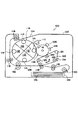
図1は本発明の画像形成装置の好適な一実施形態を示す概略構成図である。
画像形成装置100は、ケーシング102で覆われており、その上面は排出トレイ部104を兼用している。ケーシング102内には、その中央部に電子写真感光体106が配設されている。この電子写真感光体106の周囲には、直上部やや右寄りから反時計回りに、電子写真感光体106の表面を一様に帯電するための帯電装置108、露光光源として自己走査型LED(以下、「SLED」という)を備える露光装置110、現像装置116、中間転写ベルト122及びクリーニング装置124が配設されている。なお、図1には詳細を示していないが、クリーニング装置124は潤滑剤供給装置と一体化したものである。クリーニング装置124及び潤滑剤供給装置の詳細については、図13を参照して後述する。
[First Embodiment of Image Forming Apparatus]
FIG. 1 is a schematic configuration diagram showing a preferred embodiment of an image forming apparatus of the present invention.
The
電子写真感光体106は、導電性基体及び該導電性基体に形成された電荷発生層及び電荷輸送層を備える感光層を有する。なお、電子写真感光体106の詳細については後述する。
The
現像装置116は、シアン(C),マゼンタ(M),イエロー(Y),ブラック(K)の各色のトナータンク112を装備し、回転することで、順次各色のトナーロール114を電子写真感光体106と対応させることが可能なロータリ現像装置である。
The developing
また、中間転写ベルト122は、複数のローラ120に巻き掛けられて図1の矢印A方向に駆動するものであり、一次(中間)転写体として機能する。現像装置116により電子写真感光体106の外周面上に形成されたトナー像が中間転写ベルト122に転写されると、潤滑剤供給装置により電子写真感光体106の外周面に潤滑剤が供給され、当該外周面のうち転写されたトナー像を担持していた領域がクリーニング装置124により清浄化される。
The
中間転写ベルト122の下端部は、画像形成用紙(以下、単に「用紙」という)126の搬送経路の一部となっており、この下端部において、用紙126は、中間転写ベルト122とローラ118との間に挟持搬送されるようになっている。
A lower end portion of the
用紙126の搬送経路には、複数のローラ118が配設され、給紙トレイ128に積み重ねられた最上層の用紙126が枚葉装置130によって取り出され、上記中間転写体124の下端部で接触しながら搬送され、定着部132を介して上記排出トレイ部104へ送り出されるようになっている。
A plurality of
なお、中間転写ベルト122の搬送路の一部に対向する位置には、濃度センサ134が設けられ、例えばテスト用パッチ(色、濃度の見本)の濃度を検出するようになっている。
A
次に、露光装置110について詳述する。露光装置110は、SLEDを用いた光源アレイからなる。図2は、光源アレイの外観を示す斜視図である。光源アレイ140は、電子写真感光体106の軸線方向に沿って複数のチップ状のLED150が配列されたLEDアレイ(発光素子アレイ)152をさらに複数個直列に配列することで構成されている。なお、LED150の発光点は、2次元的(例えば、千鳥状)に配列していることが好ましい。この光源アレイ140は、同一のケーシング154内に治められた駆動回路156(図3参照)によって点灯制御され、画像データに応じて光ビームを走査する。
Next, the
図3には、光源アレイ140の駆動回路156の詳細が示されている。駆動回路156は、基本的には図10に示す単体の駆動回路の組み合わせである。ここでは、サイリスタ10等の詳細についての説明は省略する。
FIG. 3 shows details of the
SLEDを点灯させるトリガとしては、電圧VSが抵抗158を介して点P1(点Pに続く数字は、複数配列されたLEDの順番を示す)に印加されるようになっている。この点P1を含め全ての段の点P(1〜N(Nは正の整数))は、それぞれ抵抗160を介して、ベース線161に接続されている。ベース線161は、初段で所定の電圧を維持し、各段に行くに従い、所定電位(Vf)ずつ低下する電位(Φga)とされるようになっている。
As a trigger for turning on the SLED, the voltage VS is applied to the point P1 (the number following the point P indicates the order of the plurality of LEDs arranged) via the
また、点P(1〜N)は、LED150のアノード側に接続されている。なお、LED150のカソード側は後述する階調信号線163に接続されている。
Further, the point P (1 to N) is connected to the anode side of the
ここでΦgaの駆動回路は、図4に示されるように、上記濃度センサ134からの検出信号に基づいて、APC(オートパワーコントロール)162によるに光量指示値を受けて定電流駆動されるようになっている(定電流駆動回路)。すなわち、光量指示値は、DAコンバータ164でアナログ値に変換され、抵抗166を介して第1のコンパレータ168のマイナス側入力端に接続されている。この第1のコンパレータ168のプラス側入力端はアース(GND)されている。また、第1のコンパレータ168の出力端とマイナス側入力端とは抵抗170を介して接続されている。これにより、第1のコンパレータ168の出力は、光量指示値によって変化し、所定の電圧となる。
Here, as shown in FIG. 4, the driving circuit of Φga is driven at a constant current upon receiving a light quantity instruction value from an APC (auto power control) 162 based on a detection signal from the
ここで、この出力電圧を第2のコンパレータ172のプラス側入力端に接続し、マイナス側入力端を抵抗174を介して基準の電圧源VSSと接続し、さらに、第2のコンパレータ172の出力端をMOS型トランジスタ176へ接続することで、このMOS型トランジスタ176には、一定の電流が流れることになる。
Here, this output voltage is connected to the positive input terminal of the
なお、図4では、Φgaの駆動回路を、定電流駆動回路178としたが、図5に示されるような定電圧駆動回路180でもよい。回路構成は図4の第1のコンパレータ168の出力を用いればよいため、同一の符号を付して構成の説明を省略する。
In FIG. 4, the driving circuit of Φga is the constant current driving circuit 178, but a constant
図3に示されるように、奇数段のトランジスタQ2のエミッタは第1の制御線(V1)182に接続され、偶数段のトランジスタQ2のエミッタは第2の制御線(V2)184に接続されている。また、各段の点P(1〜N)は、LED150の一端に接続され、このLED150の他端は各段の階調信号となるパルス波を出力する階調信号線163に接続されている。この階調信号線163がローレベル(L)のときに、上記点P(1〜N)が所定の電位となっていれば、LEDは点灯する。
As shown in FIG. 3, the emitter of the odd-numbered transistor Q2 is connected to the first control line (V1) 182, and the emitter of the even-numbered transistor Q2 is connected to the second control line (V2) 184. Yes. The point P (1 to N) of each stage is connected to one end of the
図6には、階調信号線163に送られるパルス波形の生成回路200が示されている。画像処理部202から出力される階調信号(12ビット)は、積算器204に入力される。画像処理部202は、例えば、記録媒体や通信回線等から送られてきた様々な形式の画像を本実施の形態の画像形成装置100に対応する形式に変換処理する。この積算器204には、補正データ保持部206に保持された補正データ(4ビット)も入力されており、各LED150の発光点むら等が補正される。
FIG. 6 shows a
積算器で補正データが加味された補正階調信号はDAコンバータ208によってアナログ信号に変換され(濃度信号)、コンパレータ210のプラスが入力端へ入力される。
The corrected gradation signal with the correction data added by the integrator is converted into an analog signal by the DA converter 208 (density signal), and the plus of the
一方、タイミング生成部212から出力される制御信号線V1(Φ1)、V2(Φ2)には、それぞれ分岐線182A、184Aが接続され、これらの分岐線182A、184AはOR回路186へ入力する。このため、OR回路186の出力は、V1及びV2の何れか一方がアクティブのとき(ここで、ローレベル)出力がアクティブとなる。このアクティブとなった時期に同期して三角波発生回路188では、三角波が生成され、コンパレータ210のマイナス側入力端に入力されるようになっている。
On the other hand,
この動作が図7のタイムチャートに示されている。すなわち、V1(Φ1)、V2(Φ2)のORをとった信号に応じて三角波が形成される。このとき、各三角波間には、スペースaが生じ、これが、奇数LED及び偶数LEDの点灯タイミングにおいて、それぞれ順次1個ずつ点灯させるためのインタバルとなる。 This operation is shown in the time chart of FIG. That is, a triangular wave is formed according to a signal obtained by ORing V1 (Φ1) and V2 (Φ2). At this time, a space a is generated between the triangular waves, and this becomes an interval for sequentially lighting one by one at the lighting timing of the odd-numbered LED and the even-numbered LED.
この三角波に濃度信号を重ね合わせ、三角波における濃度信号より高いレベルの範囲が実際の点灯時間となり、階調信号線163に送るパルス波形を生成することができる。
By superimposing the density signal on this triangular wave, the range of the level higher than the density signal in the triangular wave becomes the actual lighting time, and a pulse waveform to be sent to the
また、図8は図3のLED駆動回路の動作タイミングチャートであり、図9は図3のLED駆動回路のLED発光状態を示す特性図である。ここでは、その詳細については省略する。 FIG. 8 is an operation timing chart of the LED drive circuit of FIG. 3, and FIG. 9 is a characteristic diagram showing the LED light emission state of the LED drive circuit of FIG. Here, the details are omitted.
なお、画像形成装置100は、電子写真感光体106上のトナー像を用紙126に直接転写するものであってもよく、電子写真感光体106上のトナー像を中間転写体に転写した後、さらに被転写媒体に転写する中間転写方式のものであってもよい。なお、中間転写体としては、図1に示した画像形成装置100では中間転写体としてベルト形状の中間転写ベルト122を用いているが、ドラム形状等の中間転写体を用いてもよい。
Note that the
次に、電子写真感光体106について詳述する。図11は、電子写真感光体の一例を示す模式断面図である。電子写真感光体106は、導電性支持体2上に下引層4、電荷発生層5、電荷輸送層6、保護層7が順次積層された機能分離型の感光層3を有するものである。
Next, the
導電性基体2の材質としては、アルミニウム、ニッケル、クロム、ステンレス鋼等の金属類;プラスチック等の基体上にアルミニウム、チタニウム、ニッケル、クロム、ステンレス、金、バナジウム、酸化錫、酸化インジウム、ITO等の薄膜を設けたもの;導電性付与剤を塗布または含浸させた紙、プラスチックフィルム等、が挙げられる。なお、図1中の電子写真感光体106の形状はドラム状であるが、シート状、プレート状等の形状を有するものであってもよい。
The material of the
導電性基体2として金属パイプ基材を用いる場合、基材の表面は素管のままであってもよく、予め鏡面切削、エッチング、陽極酸化、粗切削、センタレス研削、サンドブラスト、ウエットホーニング、着色処理などの処理が行われてもよい。基材表面を粗面化することにより可干渉光源を用いた場合に発生し得る電子写真感光体106内での干渉光による木目状の濃度斑を防止することができる。
When a metal pipe substrate is used as the
下引層4は、感光層3の帯電の際に、導電性基体2から感光層3への電荷の注入を阻止すると共に、感光層3を導電性基体2に対して一体的に接着保持せしめる接着層としての作用、あるいは場合により導電性基体2の光の反射防止作用等を有するものである。
The
下引層4の材料としては、ポリビニルブチラールなどのアセタール樹脂、ポリビニルアルコール樹脂、カゼイン、ポリアミド樹脂、セルロース樹脂、ゼラチン、ポリウレタン樹脂、ポリエステル樹脂、メタクリル樹脂、アクリル樹脂、ポリ塩化ビニル樹脂、ポリビニルアセテート樹脂、塩化ビニル−酢酸ビニル−無水マレイン酸樹脂、シリコーン樹脂、シリコーン−アルキッド樹脂、フェノール−ホルムアルデヒド樹脂、メラミン樹脂等の高分子樹脂化合物が挙げられる。また、ジルコニウムキレート化合物、チタニウムキレート化合物、アルミニウムキレート化合物、チタニウムアルコキシド化合物、有機チタニウム化合物、シランカップリング剤等を用いてもよい。また、電荷輸送性基を有する電荷輸送性樹脂やポリアニリン等の導電性樹脂などを用いることができる。これらの化合物は単独で又は2種以上の混合物若しくは重縮合物として用いることができる。これらの中でも、上層の塗布溶剤に不溶な樹脂が好ましく用いられ、特にフェノール樹脂、フェノール−ホルムアルデヒド樹脂、メラミン樹脂、ウレタン樹脂、エポキシ樹脂などが好ましく用いられる。さらに、ジルコニウムキレート化合物、シランカップリング剤は残留電位が低く環境による電位変化が少なく、また繰り返し使用による電位の変化が少ないなど性能上優れている。
Materials for the
シランカップリング剤としては、ビニルトリメトキシシラン、γ−メタクリルオキシプロピル−トリス(6−メトキシエトキシ)シラン、β−(3,4−エポキシシクロヘキシル)エチルトリメトキシシラン、γ−グリシドキシプロピルトリメトキシシラン、ビニルトリアセトキシシラン、γ−メルカプトプロピルトリメトキシシラン、γ−アミノプロピルトリエトキシシラン、N−β−(アミノエチル)−γ−アミノプロピルトリメトキシシラン、N−β−(アミノエチル)−γ−アミノプロピルメチルメトキシシラン、N,N−ビス(β−ヒドロキシエチル)−γ−アミノプロピルトリエトキシシラン、γ−クロルプロピルトリメトキシシランなどが挙げられる。これらの中でも、ビニルトリエトキシシラン、ビニルトリス(2−メトキシエトキシシラン)、3−メタクリロキシプロピルトリメトキシシラン、3−グリシドキシプロピルトリメトキシシラン、2−(3,4−エポキシシクロヘキシル)エチルトリメトキシシラン、N−2−(アミノエチル)3−アミノプロピルトリメトキシシラン、N−2−(アミノエチル)3−アミノプロピルメチルジメトキシシラン、3−アミノプロピルトリエトキシシラン、N−フェニル−3−アミノプロピルトリメトキシシラン、3−メルカプトプロピルトリメトキシシラン、3−クロロプロピルトリメトキシシランなどのシランカップリング剤が好ましい。 Examples of silane coupling agents include vinyltrimethoxysilane, γ-methacryloxypropyl-tris (6-methoxyethoxy) silane, β- (3,4-epoxycyclohexyl) ethyltrimethoxysilane, and γ-glycidoxypropyltrimethoxy. Silane, vinyltriacetoxysilane, γ-mercaptopropyltrimethoxysilane, γ-aminopropyltriethoxysilane, N-β- (aminoethyl) -γ-aminopropyltrimethoxysilane, N-β- (aminoethyl) -γ -Aminopropylmethylmethoxysilane, N, N-bis (β-hydroxyethyl) -γ-aminopropyltriethoxysilane, γ-chloropropyltrimethoxysilane and the like. Among these, vinyltriethoxysilane, vinyltris (2-methoxyethoxysilane), 3-methacryloxypropyltrimethoxysilane, 3-glycidoxypropyltrimethoxysilane, 2- (3,4-epoxycyclohexyl) ethyltrimethoxy Silane, N-2- (aminoethyl) 3-aminopropyltrimethoxysilane, N-2- (aminoethyl) 3-aminopropylmethyldimethoxysilane, 3-aminopropyltriethoxysilane, N-phenyl-3-aminopropyl Silane coupling agents such as trimethoxysilane, 3-mercaptopropyltrimethoxysilane, and 3-chloropropyltrimethoxysilane are preferred.
ジルコニウムキレート化合物としては、ジルコニウムブトキシド、ジルコニウムアセト酢酸エチル、ジルコニウムトリエタノールアミン、アセチルアセトネートジルコニウムブトキシド、アセト酢酸エチルジルコニウムブトキシド、ジルコニウムアセテート、ジルコニウムオキサレート、ジルコニウムラクテート、ジルコニウムホスホネート、オクタン酸ジルコニウム、ナフテン酸ジルコニウム、ラウリン酸ジルコニウム、ステアリン酸ジルコニウム、イソステアリン酸ジルコニウム、メタクリレートジルコニウムブトキシド、ステアレートジルコニウムブトキシド、イソステアレートジルコニウムブトキシドなどが挙げられる。 Zirconium chelate compounds include: zirconium butoxide, zirconium zirconium acetoacetate, zirconium triethanolamine, acetylacetonate zirconium butoxide, ethyl acetoacetate butoxide, zirconium acetate, zirconium oxalate, zirconium lactate, zirconium phosphonate, zirconium octoate, naphthenic acid Zirconium, zirconium laurate, zirconium stearate, zirconium isostearate, methacrylate zirconium butoxide, stearate zirconium butoxide, isostearate zirconium butoxide and the like.
チタニウムキレート化合物としては、テトライソプロピルチタネート、テトラノルマルブチルチタネート、ブチルチタネートダイマー、テトラ(2−エチルヘキシル)チタネート、チタンアセチルアセトネート、ポリチタンアセチルアセトネート、チタンオクチレングリコレート、チタンラクテートアンモニウム塩、チタンラクテート、チタンラクテートエチルエステル、チタントリエタノールアミネート、ポリヒドロキシチタンステアレートなどが挙げられる。 Titanium chelate compounds include tetraisopropyl titanate, tetranormal butyl titanate, butyl titanate dimer, tetra (2-ethylhexyl) titanate, titanium acetylacetonate, polytitanium acetylacetonate, titanium octylene glycolate, titanium lactate ammonium salt, titanium Examples include lactate, titanium lactate ethyl ester, titanium triethanolamate, and polyhydroxytitanium stearate.
アルミニウムキレート化合物としては、アルミニウムイソプロピレート、モノブトキシアルミニウムジイソプロピレート、アルミニウムブチレート、ジエチルアセトアセテート、アルミニウムジイソプロピレート、アルミニウムトリス(エチルアセトアセテート)などが挙げられる。 Examples of the aluminum chelate compound include aluminum isopropylate, monobutoxy aluminum diisopropylate, aluminum butyrate, diethyl acetoacetate, aluminum diisopropylate, and aluminum tris (ethyl acetoacetate).
下引層4中には、感光体特性向上のために、導電性物質を含有させることができる。かかる導電性物質としては、酸化チタン、酸化亜鉛、酸化錫等の金属酸化物等があげられるが、所望の感光体特性が得られるのであれば、公知のいかなるものでも使用することができる。
The
また、下引層4に用いられる金属酸化物には表面処理を施すことができる。表面処理を施すことで、抵抗値の制御、分散性制御、感光体特性向上を図ることができる。表面処理剤としては、ジルコニウムキレート化合物、チタニウムキレート化合物、アルミニウムキレート化合物、チタニウムアルコキシド化合物、有機チタニウム化合物、シランカップリング剤等の公知の材料を用いることができる。これらの化合物は単独で又は2種以上の化合物の混合物若しくは重縮合物として用いることができる。中でもシランカップリング剤は、残留電位が低く環境による電位変化が少なく、また繰り返し使用による電位の変化が少ない、画質特性に優れるなど性能上優れている。なお、シランカップリング剤、ジルコニウムキレート化合物、チタニウムキレート化合物、アルミニウムキレート化合物としては、前述した例と同じ物質が挙げられる。
The metal oxide used for the
表面処理方法は公知の方法であればいかなる方法でも使用可能であるが、乾式法あるいは湿式法を用いることができる。乾式法にて表面処理を施す場合には金属酸化物微粒子をせん断力の大きなミキサ等で攪拌しながら、直接あるいは有機溶媒に溶解させたシランカップリング剤を滴下、乾燥空気や窒素ガスとともに噴霧させることによって均一に処理される。添加あるいは噴霧する際には溶剤の沸点以下の温度で行われることが好ましい。溶剤の沸点以上の温度で噴霧すると、均一に攪拌される前に溶剤が蒸発し、シランカップリング剤が局部的にかたまってしまい均一な処理ができにくい欠点があり、好ましくない。添加あるいは噴霧した後、さらに100℃以上で焼き付けを行うことができる。焼き付けは所望の電子写真特性が得られる温度、時間であれば任意の範囲で実施できる。湿式法としては、金属酸化物微粒子を溶剤中に攪拌、超音波、サンドミルやアトライター、ボールミルなどを用いて分散し、シランカップリング剤溶液を添加し攪拌あるいは分散した後、溶剤除去することで均一に処理される。溶剤除去方法は蒸留により留去される。ろ過による除去方法では未反応のシランカップリング剤が流出しやすく、所望の特性を得るためのシランカップリング剤量をコントロールし難い欠点があり、好ましくない。溶剤除去後にはさらに100℃以上で焼き付けを行うことができる。焼き付けは所望の電子写真特性が得られる温度、時間であれば任意の範囲で実施できる。湿式法においては金属酸化物微粒子含有水分除去法として表面処理に用いる溶剤中で攪拌加熱しながら除去する方法、溶剤と共沸させて除去する方法を用いることもできる。 As the surface treatment method, any known method can be used, but a dry method or a wet method can be used. When surface treatment is performed by a dry method, a silane coupling agent dissolved directly or in an organic solvent is dropped and sprayed with dry air or nitrogen gas while stirring the metal oxide fine particles with a mixer having a large shearing force. Can be processed uniformly. The addition or spraying is preferably performed at a temperature below the boiling point of the solvent. Spraying at a temperature equal to or higher than the boiling point of the solvent is not preferred because it causes the solvent to evaporate before being stirred uniformly, causing the silane coupling agent to locally accumulate and making uniform processing difficult. After addition or spraying, baking can be performed at 100 ° C. or higher. Baking can be carried out in an arbitrary range as long as the temperature and time allow the desired electrophotographic characteristics to be obtained. As a wet method, the metal oxide fine particles are dispersed in a solvent using stirring, ultrasonic waves, a sand mill, an attritor, a ball mill, etc., and a silane coupling agent solution is added and stirred or dispersed, and then the solvent is removed. Uniformly processed. The solvent removal method is distilled off by distillation. The removal method by filtration is not preferable because unreacted silane coupling agent tends to flow out, and the amount of silane coupling agent for obtaining desired characteristics is difficult to control. After removing the solvent, baking can be performed at 100 ° C. or higher. Baking can be carried out in an arbitrary range as long as the temperature and time allow the desired electrophotographic characteristics to be obtained. In the wet method, as a method for removing the metal oxide fine particle-containing water, a method of removing with stirring and heating in a solvent used for surface treatment, or a method of removing by azeotropic distillation with a solvent can be used.
下引層4中の金属酸化物微粒子に対するシランカップリング剤の量は、所望の電子写真特性が得られる量であればいかなる量でも用いることができる。
The amount of the silane coupling agent relative to the metal oxide fine particles in the
下引層4中に用いられる金像酸化物微粒子と樹脂との割合は、所望の電子写真特性が得られる割合であれば任意に設定できる。
The ratio between the gold image oxide fine particles and the resin used in the
下引層4中には光散乱性の向上などの目的により、各種の有機もしくは無機微粉末を混合することができる。とくに、酸化チタン、酸化亜鉛、硫化亜鉛、鉛白、リトポン等の白色顔料やアルミナ、炭酸カルシウム、硫酸バリウム等の体質顔料としての無機顔料やPTFE樹脂粒子、ベンゾグアナミン樹脂粒子、スチレン樹脂粒子などが有効である。添加微粉末の粒径は0.01〜2μmのものが用いられる。微粉末は必要に応じて添加されるが、添加される場合には下引層4の固形分に対して、重量比で、好ましくは10〜80質量%、より好ましくは30〜70質量%添加される。
Various organic or inorganic fine powders can be mixed in the
また、下引層形成用塗布液には電気特性向上、環境安定性向上、画質向上のために種々の添加物を用いることができる。添加物としては、クロラニル、ブロモアニル、アントラキノン等のキノン系化合物、テトラシアノキノジメタン系化合物、2,4,7−トリニトロフルオレノン、2,4,5,7−テトラニトロ−9−フルオレノン等のフルオレノン化合物、2−(4−ビフェニル)−5−(4−t−ブチルフェニル)−1,3,4−オキサジアゾールや2,5−ビス(4−ナフチル)−1,3,4−オキサジアゾール、2,5−ビス(4−ジエチルアミノフェニル)−1,3,4オキサジアゾールなどのオキサジアゾール系化合物、キサントン系化合物、チオフェン化合物、3,3’,5,5’テトラ−t−ブチルジフェノキノン等のジフェノキノン化合物などの電子輸送性物質、多環縮合系、アゾ系等の電子輸送性顔料等を含有させることも有効である。 Various additives can be used in the coating liquid for forming the undercoat layer in order to improve electrical characteristics, environmental stability, and image quality. Additives include quinone compounds such as chloranil, bromoanil and anthraquinone, tetracyanoquinodimethane compounds, fluorenones such as 2,4,7-trinitrofluorenone and 2,4,5,7-tetranitro-9-fluorenone Compounds, 2- (4-biphenyl) -5- (4-t-butylphenyl) -1,3,4-oxadiazole and 2,5-bis (4-naphthyl) -1,3,4-oxadi Azoles, oxadiazole compounds such as 2,5-bis (4-diethylaminophenyl) -1,3,4 oxadiazole, xanthone compounds, thiophene compounds, 3,3 ′, 5,5 ′ tetra-t- It is also effective to contain an electron transporting substance such as a diphenoquinone compound such as butyldiphenoquinone, an electron transporting pigment such as a polycyclic condensation system or an azo group.
下引層塗布液の形成において、前述したような導電性物質や光散乱物質などの微粉末を混入させる場合には樹脂成分を溶解した溶液中に微粉末添加して分散処理が行われる。微粉末を樹脂中に分散させる方法としては、ロールミル、ボールミル、振動ボールミル、アトライター、サンドミル、コロイドミル、ペイントシェーカーなどの方法を用いることができる。さらにこの下引層4を設けるときに用いる塗布方法としては、ブレードコーティング法、ワイヤーバーコーティング法、スプレーコーティング法、浸漬コーティング法、ビードコーティング法、エアーナイフコーティング法、カーテンコーティング法等の通常の方法を用いることができる。
In the formation of the undercoat layer coating liquid, when the fine powder such as the conductive material or the light scattering material as described above is mixed, the fine powder is added to the solution in which the resin component is dissolved and the dispersion treatment is performed. As a method for dispersing the fine powder in the resin, methods such as a roll mill, a ball mill, a vibrating ball mill, an attritor, a sand mill, a colloid mill, and a paint shaker can be used. Further, as the coating method used when the
下引層4の膜厚は、好ましくは0.01〜50μm、より好ましくは0.05〜30μmである。
The film thickness of the
次に、電荷発生層5について説明する。電荷発生層5は、電荷発生材料及び結着樹脂を含んで構成される。結着樹脂としては、広範な絶縁性樹脂から選択することができる、また、ポリ−N−ビニルカルバゾール、ポリビニルアントラセン、ポリビニルピレン、ポリシランなどの有機光導電性ポリマーから選択することもできる。好ましい結着樹脂としては、ポリビニルブチラール樹脂、ポリアリレート樹脂(ビスフェノールAとフタル酸の重縮合体等)、ポリカーボネート樹脂、ポリエステル樹脂、フェノキシ樹脂、塩化ビニル−酢酸ビニル共重合体、ポリアミド樹脂、アクリル樹脂、ポリアクリルアミド樹脂、ポリビニルピリジン樹脂、セルロース樹脂、ウレタン樹脂、エポキシ樹脂、カゼイン、ポリビニルアルコール樹脂、ポリビニルピロリドン樹脂等の絶縁性樹脂を挙げることができるが、これらに限定されるものではない。これらの結着樹脂は、単独あるいは2種以上混合して用いることができる。
Next, the
電荷発生材料としては特に制限されないが、金属及び無金属フタロシアニン顔料が好ましく、中でも特定の結晶を有するヒドロキシガリウムフタロシアニン、クロロガリウムフタロシアニン、ジクロロスズフタロシアニン、チタニルフタロシアニンが特に好ましい。 The charge generation material is not particularly limited, but metal and metal-free phthalocyanine pigments are preferable, and hydroxygallium phthalocyanine, chlorogallium phthalocyanine, dichlorotin phthalocyanine, and titanyl phthalocyanine having specific crystals are particularly preferable.
電荷発生材料と結着樹脂の配合比は(質量比)は10:1〜1:10の範囲が好ましい。またこれらを分散させる方法としてはボールミル分散法、アトライター分散法、サンドミル分散法等の通常の方法を用いることができるが、この際、分散によって該の結晶型が変化しない条件が必要とされる。なお、本実施形態においては、上記分散法のいずれについても分散前と結晶型が変化していないことを確認している。さらにこの分散の際、粒子を0.5μm以下、好ましくは0.3μm以下、さらに好ましくは0.15μm以下の粒子サイズにすると有効である。また、これらの分散に用いる溶剤としては、メタノール、エタノール、n−プロパノール、n−ブタノール、ベンジルアルコール、メチルセルソルブ、エチルセルソルブ、アセトン、メチルエチルケトン、シクロヘキサノン、酢酸メチル、酢酸n−ブチル、ジオキサン、テトラヒドロフラン、メチレンクロライド、クロロホルム、クロルベンゼン、トルエン等の通常の有機溶剤を単独で又は2種以上混合して用いることができる。また、本実施形態における電荷発生層5の膜厚は、一般的に0.1〜5μm、好ましくは0.2〜2.0μmである。また、電荷発生層5を設けるときに用いる塗布方法としては、ブレードコーティング法、マイヤーバーコーティング法、スプレーコーティング法、浸漬コーティング法、ビードコーティング法、エアーナイフコーティング法、カーテンコーティング法等の通常の方法を用いることができる。さらに、顔料の分散安定性や、光感度を増す目的、あるいは、電気特性を安定化させる目的でシランカップリング剤を用いて顔料を表面処理したものを用いてもよいし、顔料の分散溶液に加えてもよい。
The mixing ratio of the charge generation material and the binder resin (mass ratio) is preferably in the range of 10: 1 to 1:10. In addition, as a method for dispersing these, a usual method such as a ball mill dispersion method, an attritor dispersion method, a sand mill dispersion method, or the like can be used. . In the present embodiment, it is confirmed that the crystal form is not changed from that before dispersion in any of the above dispersion methods. Further, in this dispersion, it is effective that the particles have a particle size of 0.5 μm or less, preferably 0.3 μm or less, more preferably 0.15 μm or less. Moreover, as a solvent used for these dispersions, methanol, ethanol, n-propanol, n-butanol, benzyl alcohol, methyl cellosolve, ethyl cellosolve, acetone, methyl ethyl ketone, cyclohexanone, methyl acetate, n-butyl acetate, dioxane, Usual organic solvents such as tetrahydrofuran, methylene chloride, chloroform, chlorobenzene and toluene can be used alone or in admixture of two or more. Further, the film thickness of the
次に、電荷輸送層6について説明する。電荷輸送層6は、電荷輸送材料と結着樹脂を含有して形成されるか、あるいは高分子電荷輸送材を含有して形成される。 Next, the charge transport layer 6 will be described. The charge transport layer 6 is formed containing a charge transport material and a binder resin, or is formed containing a polymer charge transport material.
電荷輸送材料としては、p−ベンゾキノン、クロラニル、ブロマニル、アントラキノン等のキノン系化合物、テトラシアノキノジメタン系化合物、2,4,7−トリニトロフルオレノン等のフルオレノン化合物、キサントン系化合物、ベンゾフェノン系化合物、シアノビニル系化合物、エチレン系化合物等の電子輸送性化合物、トリアリールアミン系化合物、ベンジジン系化合物、アリールアルカン系化合物、アリール置換エチレン系化合物、スチルベン系化合物、アントラセン系化合物、ヒドラゾン系化合物などの正孔輸送性化合物が挙げられる。これらの電荷輸送材料は、単独で又は2種以上混合して用いることができるが、これらに限定されるものではない。 Examples of charge transport materials include quinone compounds such as p-benzoquinone, chloranil, bromanyl, anthraquinone, tetracyanoquinodimethane compounds, fluorenone compounds such as 2,4,7-trinitrofluorenone, xanthone compounds, benzophenone compounds Electron transporting compounds such as cyanovinyl compounds and ethylene compounds, triarylamine compounds, benzidine compounds, arylalkane compounds, aryl-substituted ethylene compounds, stilbene compounds, anthracene compounds, hydrazone compounds, etc. Examples thereof include pore transporting compounds. These charge transport materials can be used alone or in combination of two or more, but are not limited thereto.
電荷輸送層6の形成に用いる結着樹脂としては、ポリカーボネート樹脂、ポリエステル樹脂、メタクリル樹脂、アクリル樹脂、ポリ塩化ビニル樹脂、ポリ塩化ビニリデン樹脂、ポリスチレン樹脂、ポリビニルアセテート樹脂、スチレン−ブタジエン共重合体、塩化ビニリデン−アクリロニトリル共重合体、塩化ビニル−酢酸ビニル共重合体、塩化ビニル−酢酸ビニル−無水マレイン酸共重合体、シリコーン樹脂、シリコン−アルキッド樹脂、フェノール−ホルムアルデヒド樹脂、スチレン−アルキッド樹脂や、ポリ−N−ビニルカルバゾール、ポリシラン、特開平8−176293号公報や特開平8−208820号公報に示されているポリエステル系高分子電荷輸送材など高分子電荷輸送材を用いることもできる。本実施形態にかかる電荷輸送層6の膜厚は、一般的に5〜50μm、好ましくは15〜22μmである。塗布方法としては、ブレードコーティング法、マイヤーバーコーティング法、スプレーコーティング法、浸漬コーティング法、ビードコーティング法、エアーナイフコーティング法、カーテンコーティング法等の通常の方法を用いることができる。さらに電荷輸送層を設けるときに用いる溶剤としては、ベンゼン、トルエン、キシレン、クロルベンゼン等の芳香族炭化水素類、アセトン、2−ブタノン等のケトン類、塩化メチレン、クロロホルム、塩化エチレン等のハロンゲン化脂肪族炭化水素類、テトラヒドロフラン、エチルエーテル等の環状もしくは直鎖状のエーテル類等通常の有機溶剤を単独で又は2種以上混合して用いることができる。通常は、これらの材料を混合して塗布液を熱風乾燥し、電荷輸送層6を形成する。 As the binder resin used for forming the charge transport layer 6, polycarbonate resin, polyester resin, methacrylic resin, acrylic resin, polyvinyl chloride resin, polyvinylidene chloride resin, polystyrene resin, polyvinyl acetate resin, styrene-butadiene copolymer, Vinylidene chloride-acrylonitrile copolymer, vinyl chloride-vinyl acetate copolymer, vinyl chloride-vinyl acetate-maleic anhydride copolymer, silicone resin, silicon-alkyd resin, phenol-formaldehyde resin, styrene-alkyd resin, poly Polymeric charge transport materials such as -N-vinylcarbazole, polysilane, and polyester-based polymer charge transport materials disclosed in JP-A-8-176293 and JP-A-8-208820 can also be used. The film thickness of the charge transport layer 6 according to this embodiment is generally 5 to 50 μm, preferably 15 to 22 μm. As a coating method, a normal method such as a blade coating method, a Meyer bar coating method, a spray coating method, a dip coating method, a bead coating method, an air knife coating method, or a curtain coating method can be used. Furthermore, as a solvent used when providing a charge transport layer, aromatic hydrocarbons such as benzene, toluene, xylene and chlorobenzene, ketones such as acetone and 2-butanone, and halogenation such as methylene chloride, chloroform and ethylene chloride Ordinary organic solvents such as aliphatic hydrocarbons, cyclic or linear ethers such as tetrahydrofuran and ethyl ether can be used alone or in admixture of two or more. Usually, the charge transport layer 6 is formed by mixing these materials and drying the coating liquid with hot air.
画像形成装置100中で発生するオゾンや酸化性ガス、或いは光・熱による感光体106の劣化を防止する目的で、感光層中に酸化防止剤・光安定剤・熱安定剤などの添加剤を添加することができる。例えば、酸化防止剤としては、ヒンダードフェノール、ヒンダードアミン、パラフェニレンジアミン、アリールアルカン、ハイドロキノン、スピロクロマン、スピロインダノンおよびそれらの誘導体、有機硫黄化合物、有機リン化合物等があげられる。光安定剤の例としては、ベンゾフェノン、ベンゾアゾール、ジチオカルバメート、テトラメチルピペン等の誘導体が挙げられる。
Additives such as antioxidants, light stabilizers, and heat stabilizers in the photosensitive layer for the purpose of preventing deterioration of the
次に保護層7について説明する。保護層7は、帯電時の電荷輸送層6等の化学的変化を防止したり、感光層3の機械的強度をさらに改善したりする機能を有するもので、例えば導電性材料を適当な結着樹脂中に含有させて構成される。
Next, the
保護層7の形成に用いる導電性材料としては、N,N'−ジメチルフェロセン等のメタロセン化合物、N,N'−ジフェニル−N,N'−ビス(3−メチルフェニル)−[1,1'−ビフェニル]−4,4'−ジアミン等の芳香族アミン化合物、酸化モリブデン、酸化タングステン、酸化アンチモン、酸化錫、酸化チタン、酸化インジウム、酸化錫とアンチモンあるいは酸化アンチモンとの固溶体の担体またはこれらの混合物、あるいは単一粒子中にこれらの金属酸化物を混合したもの、あるいは被覆したものが挙げられるが、これらに限定されるものではない。
Examples of the conductive material used for forming the
保護層125の形成に用いる結着樹脂としては、ポリアミド樹脂、ポリビニルアセタール樹脂、ポリウレタン樹脂、ポリエステル樹脂、エポキシ樹脂、ポリケトン樹脂、ポリカーボネート樹脂、ポリビニルケトン樹脂、ポリスチレン樹脂、ポリアクリルアミド樹脂、ポリイミド樹脂、ポリアミドイミド樹脂等が挙げられ、これらは必要に応じて架橋して使用することもできる。さらに電荷輸送性を有し、架橋構造を有するシロキサン系樹脂を保護層として使用することもできる。電荷輸送性化合物を含むシロキサン樹脂硬化膜の場合、電荷輸送性化合物として公知の材料であればいかなるものでも使用可能であるが、例えば特開平10−95787号公報、特開平10−251277号公報、特開平11−32716号公報、特開平11−38656号公報、特開平11−236391号公報に示された化合物等が挙げられるがこれに限定されるものではない。 As the binder resin used for forming the protective layer 125, polyamide resin, polyvinyl acetal resin, polyurethane resin, polyester resin, epoxy resin, polyketone resin, polycarbonate resin, polyvinyl ketone resin, polystyrene resin, polyacrylamide resin, polyimide resin, polyamide Examples thereof include imide resins, and these can be used after being crosslinked. Furthermore, a siloxane-based resin having a charge transporting property and having a crosslinked structure can be used as the protective layer. In the case of a cured siloxane resin film containing a charge transporting compound, any known material can be used as the charge transporting compound. For example, JP-A-10-95787, JP-A-10-251277, Examples thereof include, but are not limited to, compounds disclosed in JP-A-11-32716, JP-A-11-38656, and JP-A-11-236391.
本実施形態にかかる電子写真感光体106は、電子写真プロセスを400,000サイクル繰り返したとき、感光層3の平均摩耗率が1,000サイクル当たり15nm以下、好ましくは12nm以下、より好ましくは9nm以下である。さらに、該感光層3の画像形成領域における膜厚の最大値と最小値との差が、電子写真プロセスを行う前の電荷輸送層6の平均膜厚の15%以下、好ましくは12%以下、より好ましくは9%以下である。これにより、高画質化、高速化及び長寿命化をより高水準で達成することができる。
In the
また、電子写真感光体106表面の線速度は、高速化の観点から、好ましくは100mm/秒以上、より好ましくは120mm/秒以上、更に好ましくは150mm/秒以上である。さらに、電子写真感光体106の回転方向における画像解像度は、高解像度化及び高画質化の観点から、好ましくは1200dpi以上、より好ましくは1800dpi以上、更に好ましくは2400dpi以上である。
The linear velocity on the surface of the electrophotographic
また、本実施形態にかかる画像形成装置100においては、必要に応じて潤滑油供給装置及びクリーニング装置124を備えることができる。潤滑油供給装置及びクリーニング装置124を備えることで、電子写真感光体106の摩耗を抑制することができる。加えて、感光層3の構成材料の種類、後述する潤滑剤供給装置からの潤滑剤の供給量、クリーニング装置124と電子写真感光体106との接触圧力などを選定することにより、電子写真感光体106の機械的又は化学的強度を更に高めることができる。
Further, the
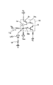
次に、潤滑油供給装置について詳述する。図12は潤滑剤供給装置の要部を示す分解斜視図である。図示の通り、潤滑剤供給装置200は、回転ブラシ212、支持部材216、ネジリバネコイル217及び2個の軸受部材218を有する。
Next, the lubricating oil supply device will be described in detail. FIG. 12 is an exploded perspective view showing a main part of the lubricant supply device. As illustrated, the
回転ブラシ212は、電子写真感光体106の回転軸(第1軸)に平行な軸部212a(第2軸)を中心として回転自在に設けられており、そのブラシ先端が電子写真感光体106の外周面に接触するように配置されている。回転ブラシ212は、軸部212aの両端を軸受部材218の軸孔218aに通すことにより回転自在に支持されている。回転ブラシ212の回転方向は、電子写真感光体106との接触位置において同一方向であることが好ましい。また、回転ブラシ212の回転速度は、電子写真感光体106との接触位置において、回転ブラシ212先端の移動速度が電子写真感光体106の外周面の移動速度よりも大きくなるように設定することが好ましい。
The
支持部材216は、板状の支持部216aと、支持部216aの後部側(感光体106と反対側)の端部に設けられた軸部216bとで構成される。固形潤滑剤214は支持部216aの回転ブラシ212側の面に取り付けられる。固形潤滑剤214としては、脂肪酸金属塩及びポリテトラフルオロエチレンが好ましく使用される。また、軸部216bはその両端部が軸受部材218の軸孔218bに通されることで軸部2aに平行な第3軸として機能し、支持部材216は軸部216bを支点として揺動自在に支持される。
The
軸部216bの回りには、支持部216aの自重および固形潤滑剤214の重力により、軸部216bの回りに支持部材216から回転ブラシ212に向かうモーメントが発生する。かかるモーメントにより固形潤滑剤214は回転ブラシ212に所定の圧力で接触する。この圧力の強さは、支持部216aの重量および固形潤滑剤214の重量が大きい程大きくなるので、これらの値を適宜設定することにより固形潤滑剤214の回転ブラシ212に対する接触圧力を設定できる。また、支持部216aの固形潤滑剤214と反対側の面上に錘を取り付けてモーメントを大きくすることもできる。
Around the
また、ネジリバネコイル217は、固形潤滑剤214の回転ブラシ212に対する接触圧力をより大きくするためのもので、支持部216aの固形潤滑剤214と反対側の面に当接配置されている。なお、支持部216aの自重および固形潤滑剤214の重力により十分なモーメントを発生させることができる場合には、ネジリバネコイル217を用いなくともよい。
Further, the
上記構成を有する潤滑剤供給装置200においては、回転ブラシ212を固体潤滑剤214に接触させて回転させることにより、回転ブラシ212に付着した潤滑剤が電子写真感光体106に塗布される。固形潤滑剤214の消費量は、電子写真感光体106の外周面に十分な潤滑性が付与される限りにおいて特に制限されないが、例えば、被転写媒体としてA4サイズの用紙を用いる場合、固形潤滑剤214の消費量は当該用紙1枚当たり2〜15μg(単位面積当たり7.6〜57ng/cm2)であることが好ましい。
In the
また、潤滑剤供給装置200による潤滑剤の供給の際、支持部材216は軸部216bの周方向以外の動きが規制されているので、固形潤滑剤214の回転ブラシ212に対するニップ量(食い込み量)は軸部216bに沿った方向において実質的に一定となる。そのため、固形潤滑剤214の消費量、すなわち回転ブラシ212に付着する固形潤滑剤214の量が軸方向で均一となり、さらには電子写真感光体106の外周面に塗布される潤滑剤の量も均一となる。従って、電子写真感光体106の外周面に高水準の潤滑性を長期にわたって安定的に付与することができ、電子写真感光体106(感光層)の摩耗による電位変動や感度変動を十分に防止することができる。また、かかる潤滑性により、後段のクリーニングブレードの摩耗や欠けが生じにくくなるため、クリーニング性を長期にわたって高水準に維持することができる。
Further, when the lubricant is supplied by the
また、固形潤滑剤214を支持する支持部材216は、軸部216bの回りにモーメントを生じさせるので、固形潤滑剤214をモーメントにより回転ブラシ212に所定の接触圧で接触させることができ、これにより、回転ブラシ212の回転による固形潤滑剤214の跳ね上がり等のランダムな動きを抑制することができるため、一定のニップ量で長期にわたり安定した固形潤滑剤214の供給ができる。したがって、固形潤滑剤214の供給量を増加させる場合であっても、当該潤滑剤の安定供給が有効に実施可能となる。
Further, since the
なお、回転ブラシ212に付着したトナーはフリッカ(図示せず)で払われ、トナー搬送オーガ(図示せず)により回収される。
The toner attached to the
次に、クリーニング装置124について詳述する。図13は、クリーニング装置の一例を示す概略構成図である。クリーニング装置124は、転写工程後の電子写真感光体106の表面に付着する残存トナーを除去するためのもので、これにより清浄面化された電子写真感光体106は電子写真プロセスに繰り返し供される。
Next, the
本実施形態にかかるクリーニング装置124は、潤滑剤供給装置200と一体化したものであり、ハウジング50の前部の回転ブラシ212よりも下流側にクリーニングブレード222が取り付けられている点以外は図11に示した潤滑油供給装置と同様の構成を有している。また、クリーニング装置124は、回転ブラシ212により電子写真感光体106に固形潤滑剤214を塗布し、クリーニングブレード222の接触抵抗を小さくする。そして、回転ブラシ212に付着したトナーはフリッカ(図示せず)で払われ、トナー搬送オーガ(図示せず)により回収される。クリーニング装置124としては、クリーニングブレードの他、ブラシクリーニング、ロールクリーニング等を用いることができるが、これらの中でもクリーニングブレードを用いることが好ましい。また、クリーニングブレードの材質としてはウレタンゴム、ネオプレンゴム、シリコーンゴム等が挙げられる。
The
このように本実施形態では、SLEDを備える露光装置110及び電子写真感光体106を組み合わせることで、感光層3の摩耗量及び膜厚ムラの制御が容易になる。加えて、更に潤滑剤供給装置200及びクリーニング装置124を組み合わせることで、電子写真プロセスを行うに際し、供給される潤滑剤により電子写真感光体106の外周面の潤滑性が高められると共にクリーニング装置124により当該表面が十分に清浄化される。これにより、感光層3の摩耗を抑制して電位変動及び感度変動を十分に防止することができる。従って本発明により、可変光量が小さく制御幅が狭いという自己走査型LEDの特性が補完され、高画質化、高速化及び長寿命化をバランスよく高水準で達成可能な画像形成装置が実現される。
As described above, in this embodiment, by combining the
なお、本発明は上記実施形態に限定されるものではない。例えば、電子写真感光体106としては、図11に示した積層構造を有するものに限定されるものではなく、十分な電子写真特性が得られる場合には、下引層4や保護層7は設けなくてもよい。
The present invention is not limited to the above embodiment. For example, the
また、図12に示した潤滑剤供給装置は支持部216aと軸部216bとが一体化した支持部材216を備えるものであるが、第3軸に相当する軸を軸受部材218に固定し、支持部材に貫通孔を設けることで、支持部材が軸から独立して揺動自在とすることもできる。
12 includes a
また、図1中に示した画像形成装置100においては、潤滑剤供給装置とクリーニング装置124とが一体化したものであるが、潤滑剤供給装置とクリーニング供給装置とを別個に設けてもよい。
In the
[画像形成装置の第2実施形態]
次に、画像形成装置の第2実施形態について説明する。なお、第1実施形態と同一又は同等の構成要素については同一符号を付し、重複する説明を省略する。
[Second Embodiment of Image Forming Apparatus]
Next, a second embodiment of the image forming apparatus will be described. In addition, the same code | symbol is attached | subjected about the component same or equivalent to 1st Embodiment, and the overlapping description is abbreviate | omitted.
本実施形態にかかる画像形成装置は、図1に示す画像形成装置と同様の構成を有するものであり、潤滑剤供給装置及びクリーニング装置124を必須要素とする点で相違する。すなわち、本実施形態に係る画像形成装置100は、電子写真感光体106、露光装置110、潤滑油供給装置及びクリーニング装置124を含んで構成されている。なお、露光装置110、潤滑油供給装置及びクリーニング装置124の構成及び配置は、第1実施形態において説明した通りである。
The image forming apparatus according to the present embodiment has the same configuration as that of the image forming apparatus shown in FIG. 1 and is different in that the lubricant supply device and the
電子写真感光体106は、図11に示すような機能分離型の感光層3を有するものに限定されるものではなく、電荷発生材料と電荷輸送材料とを同一の層に含む単層型の感光層3を有するものであってもよい。また、十分な電子写真特性が得られる場合には、下引層4や保護層7は設けなくてもよい。
The electrophotographic
さらに、本実施形態にかかる電子写真感光体106においても、電子写真プロセスを400,000サイクル繰り返したとき、感光層3の平均摩耗率が1,000サイクル当たり15nm以下が好ましく、12nm以下がより好ましく、9nm以下が更に好ましい。さらに、該感光層3の画像形成領域における膜厚の最大値と最小値との差は、電子写真プロセスを行う前の電荷輸送層6の平均膜厚の15%以下が好ましく、12%以下がより好ましく、9%以下が更に好ましい。これにより、高画質化、高速化及び長寿命化をより高水準で達成することができる。
Furthermore, also in the
また、電子写真感光体106表面の線速度は、高速化の観点から、好ましくは100mm/秒以上、より好ましくは120mm/秒以上、更に好ましくは150mm/秒以上である。さらに、電子写真感光体106の回転方向における画像解像度は、高解像度化及び高画質化の観点から、好ましくは1200dpi以上、より好ましくは1800dpi以上、更に好ましくは2400dpi以上である。
The linear velocity on the surface of the electrophotographic
このように本実施形態では、SLEDを備える露光装置110、潤滑剤供給装置200及びクリーニング装置124を組み合わせることで、電子写真プロセスを行うに際し、供給される潤滑剤により電子写真感光体106の外周面の潤滑性が高められると共にクリーニング装置124により当該表面が十分に清浄化されるので、感光層3の摩耗を抑制して電位変動及び感度変動を十分に防止することができる。従って本発明により、可変光量が小さく制御幅が狭いという自己走査型LEDの特性が補完され、高画質化、高速化及び長寿命化をバランスよく高水準で達成可能な画像形成装置が実現される。
As described above, in this embodiment, by combining the
[プロセスカートリッジの第1実施形態]
次に、プロセスカートリッジについて説明する。本実施形態にかかるプロセスカートリッジは、電子写真感光体と、露光装置とを備えるものである。
[First Embodiment of Process Cartridge]
Next, the process cartridge will be described. The process cartridge according to the present embodiment includes an electrophotographic photosensitive member and an exposure device.
図13は、プロセスカートリッジの好適な実施形態を示す概略図である。図13に示すように、プロセスカートリッジ300はケーシング311を備えており、ケーシング311の内側には、電子写真感光体106が配置されている。また、ケーシング311の内側であって、電子写真感光体106の周囲には順次、帯電装置108、露光装置110及びクリーニング装置124が配置されている。電子写真感光体106、帯電装置108、露光装置110及びクリーニング装置124の構成は、上記画像形成装置の第1実施形態において説明した通りである。また、潤滑油供給装置は、図12に示すようにクリーニング装置124内に収容されている。
FIG. 13 is a schematic view showing a preferred embodiment of a process cartridge. As shown in FIG. 13, the
このように本実施形態にかかるプロセスカートリッジ300は、SLEDを備える露光装置110及び電子写真感光体106を組み合わせることで、感光層3の摩耗量及び膜厚ムラの制御が容易になる。加えて、更に潤滑剤供給装置200及びクリーニング装置124を組み合わせることで、電子写真プロセスを行うに際し、供給される潤滑剤により電子写真感光体106の外周面の潤滑性が高められると共にクリーニング装置124により当該表面が十分に清浄化される。これにより、感光層3の摩耗を抑制して電位変動及び感度変動を十分に防止することができる。従って本発明により、可変光量が小さく制御幅が狭いという自己走査型LEDの特性が補完され、高画質化、高速化及び長寿命化をバランスよく高水準で達成可能なプロセスカートリッジが実現される。
As described above, the
[プロセスカートリッジの第2実施形態]
次に、画像形成装置の第2実施形態について説明する。なお、第1実施形態と同一又は同等の構成要素については同一符号を付し、重複する説明を省略する。
[Second Embodiment of Process Cartridge]
Next, a second embodiment of the image forming apparatus will be described. In addition, the same code | symbol is attached | subjected about the component same or equivalent to 1st Embodiment, and the overlapping description is abbreviate | omitted.
本実施形態にかかるプロセスカートリッジは、図13に示すプロセスカートリッジと同様の構成を有するものであり、潤滑剤供給装置及びクリーニング装置124を必須要素とする点で相違する。すなわち、本実施形態に係るプロセスカートリッジ300は、電子写真感光体106、露光装置110、潤滑油供給装置及びクリーニング装置124を含んで構成されている。なお、露光装置110、潤滑油供給装置及びクリーニング装置124の構成及び配置は、第1実施形態において説明した通りである。
The process cartridge according to the present embodiment has the same configuration as the process cartridge shown in FIG. 13 and is different in that the lubricant supply device and the
電子写真感光体106は、図11に示すような機能分離型の感光層3を有するものに限定されるものではなく、電荷発生材料と電荷輸送材料とを同一の層に含む単層型の感光層3を有するものであってもよい。また、十分な電子写真特性が得られる場合には、下引層4や保護層7は設けなくてもよい。
The electrophotographic
また、本実施形態にかかる電子写真感光体106においては、電子写真プロセスを400,000サイクル繰り返したとき、感光層3の平均摩耗率が1,000サイクル当たり15nm以下が好ましく、12nm以下がより好ましく、9nm以下が更に好ましい。さらに、該感光層3の画像形成領域における膜厚の最大値と最小値との差は、電子写真プロセスを行う前の電荷輸送層6の平均膜厚の15%以下が好ましく、12%以下がより好ましく、9%以下が更に好ましい。これにより、高画質化、高速化及び長寿命化をより高水準で達成することができる。
In the
さらに、電子写真感光体106の線速度は、高速化の観点から、100mm/秒以上であることが好ましく、120mm/秒以上であることがより好ましく、150mm/秒以上であることが更に好ましい。また、電子写真感光体106の回転方向における画像解像度は、高解像度化及び高画質化の観点から、1200dpi以上であることが好ましく、1800dpi以上であることがより好ましく、2400dpi以上であることが更に好ましい。
Furthermore, the linear velocity of the electrophotographic
このように本実施形態にかかるプロセスカートリッジは300、SLEDを備える露光装置110、潤滑剤供給装置及びクリーニング装置124を備えることで、感光層3の摩耗を抑制することが可能になるため、高画質化、高速化及び長寿命化を高水準でバランスよく達成可能な自己走査型LEDアレイ方式のプロセスカートリッジを実現することができる。
As described above, the process cartridge according to the present embodiment includes 300, the
以下、実施例及び比較例に基づき本発明をさらに具体的に説明するが、本発明は以下の実施例に何ら限定されるものではない。 EXAMPLES Hereinafter, although this invention is demonstrated more concretely based on an Example and a comparative example, this invention is not limited to a following example at all.
(電子写真感光体1の作製)
ホーニング処理を施した円筒状アルミニウム基体(外径30mm、長さ340mm、肉厚1mm)を準備した。次に、ジルコニウム化合物(商品名:オルガノチックスZC540、マツモト製薬社製)20質量部、シランカップリング剤(商品名:A1100、日本ユニカー社製)2.5質量部、ポリビニルブチラール樹脂(商品名:エスレックBM−S、積水化学社製)2質量部、及びブタノール43質量部を混合して下引層形成用塗布液を調製した。この塗布液をアルミニウム基体の外周面に浸漬コーティング法で塗布して、150℃にて10分間加熱乾燥し、膜厚1.0μmの下引層を形成した。
(Preparation of electrophotographic photoreceptor 1)
A hoisted cylindrical aluminum base (outer diameter 30 mm, length 340 mm, wall thickness 1 mm) was prepared. Next, 20 parts by mass of a zirconium compound (trade name: Organochix ZC540, manufactured by Matsumoto Pharmaceutical Co., Ltd.), 2.5 parts by mass of a silane coupling agent (trade name: A1100, manufactured by Nihon Unicar Company), polyvinyl butyral resin (trade name: An undercoat layer forming coating solution was prepared by mixing 2 parts by mass of ESREC BM-S (manufactured by Sekisui Chemical Co., Ltd.) and 43 parts by mass of butanol. This coating solution was applied to the outer peripheral surface of the aluminum substrate by a dip coating method and dried by heating at 150 ° C. for 10 minutes to form an undercoat layer having a thickness of 1.0 μm.
次に、X線回折スペクトルにおけるブラッグ角(2θ±0.2°)が、7.3°、16.0°、24.9°及び28.0°に回折ピークを持つヒドロキシガリウムフタロシアニン15質量部、結着樹脂としての塩化ビニル−酢酸ビニル共重合樹脂(VMCH、日本ユニカー社製)10質量部、及び酢酸n−ブチル300質量部を混合して、ガラスビーズと共に横型サンドミルで0.5時間分散し電荷発生層形成用塗布液を調製した。得られた塗布液を下引層上に浸漬コートして、100℃にて10分間加熱乾燥し、膜厚約0.15μmの電荷発生層を形成した。 Next, 15 parts by mass of hydroxygallium phthalocyanine having diffraction peaks at X-ray diffraction spectra at Bragg angles (2θ ± 0.2 °) of 7.3 °, 16.0 °, 24.9 ° and 28.0 ° , 10 parts by weight of vinyl chloride-vinyl acetate copolymer resin (VMCH, manufactured by Nihon Unicar Co., Ltd.) as a binder resin and 300 parts by weight of n-butyl acetate were mixed and dispersed with glass beads for 0.5 hour in a horizontal sand mill. Then, a coating solution for forming a charge generation layer was prepared. The obtained coating solution was dip-coated on the undercoat layer and dried by heating at 100 ° C. for 10 minutes to form a charge generation layer having a thickness of about 0.15 μm.
次に、下記式(1)で示される化合物を2質量部、下記式(2)で示される化合物15質量部、及び下記式(3)で表される高分子化合物(粘度平均分子量39,000)55質量部をテトラヒドロフラン75質量部及びクロロベンゼン25質量部の混合溶剤に溶解させて電荷輸送層形成用塗布液を調製した。得られた塗布液を電荷発生層上に浸漬コーティング法で塗布して、135℃にて40分間熱風乾燥し、膜厚32μmの電荷輸送層を形成した。このようにして電子写真感光体1を得た。

(電子写真感光体2の作製)
円筒状アルミニウム基体(外径30mm、長さ340mm、肉厚1mm)を準備した。次に、酸化亜鉛(平均粒径70μm、テイカ社製)100質量部をトルエン500質量部と攪拌混合した後、シランカップリング剤(商品名:KBM603、信越化学社製)1.5質量部を添加して2時間攪拌した。次に、トルエンを減圧蒸留にて溜去し、150℃で2時間焼き付けを行って表面処理が施された酸化亜鉛を得た。次に、表面処理を施した酸化亜鉛60質量部、硬化剤(ブロックイソシアネート、商品名:スミジュール3175、住友バイエルンウレタン社製)15質量部、及びブチラール樹脂(商品名:BM−1、積水化学社製)15質量部をメチルエチルケトン85質量部に溶解した。次に、この溶液38質量部とメチルエチルケトン25質量部とを混合して、1mmφのガラスビーズを用いてサンドミルにて2時間の分散処理を行い、分散液を得た。得られた分散液に触媒としてのジオクチルスズジラウレート0.005質量部を添加し、下引層形成用塗布液を得た。この塗布液を浸漬コーティング法にてアルミニウム基体上に塗布して、160℃にて100分間乾燥硬化を行い、膜厚20μmの下引層を形成した。
(Preparation of electrophotographic photoreceptor 2)
A cylindrical aluminum substrate (outer diameter 30 mm, length 340 mm, wall thickness 1 mm) was prepared. Next, 100 parts by mass of zinc oxide (average particle size 70 μm, manufactured by Teica) was stirred and mixed with 500 parts by mass of toluene, and then 1.5 parts by mass of a silane coupling agent (trade name: KBM603, manufactured by Shin-Etsu Chemical Co., Ltd.) Added and stirred for 2 hours. Next, toluene was distilled off under reduced pressure and baked at 150 ° C. for 2 hours to obtain zinc oxide that had been surface-treated. Next, 60 parts by mass of surface-treated zinc oxide, 15 parts by mass of a curing agent (block isocyanate, trade name: Sumidur 3175, manufactured by Sumitomo Bayern Urethane Co., Ltd.), and butyral resin (trade name: BM-1, Sekisui Chemical) 15 parts by mass) were dissolved in 85 parts by mass of methyl ethyl ketone. Next, 38 parts by mass of this solution and 25 parts by mass of methyl ethyl ketone were mixed and subjected to a dispersion treatment for 2 hours with a sand mill using glass beads of 1 mmφ to obtain a dispersion. To the obtained dispersion, 0.005 part by mass of dioctyltin dilaurate as a catalyst was added to obtain a coating liquid for forming an undercoat layer. This coating solution was applied onto an aluminum substrate by a dip coating method, followed by drying and curing at 160 ° C. for 100 minutes to form an undercoat layer having a thickness of 20 μm.
次に、X線回折スペクトルにおけるブラッグ角(2θ±0.2°)が、7.3°、16.0°、24.9°及び28.0°に回折ピークを持つヒドロキシガリウムフタロシアニン15質量部、結着樹脂としての塩化ビニル−酢酸ビニル共重合樹脂(VMCH、日本ユニカー社製)10質量部、及び酢酸n−ブチル300質量部を混合して、ガラスビーズと共に横型サンドミルで0.5時間分散し電荷発生層形成用塗布液を調製した。得られた塗布液を下引層上に浸漬コートして、100℃にて10分間加熱乾燥し、膜厚約0.15μmの電荷発生層を形成した。 Next, 15 parts by mass of hydroxygallium phthalocyanine having diffraction peaks at X-ray diffraction spectra at Bragg angles (2θ ± 0.2 °) of 7.3 °, 16.0 °, 24.9 °, and 28.0 ° , 10 parts by weight of vinyl chloride-vinyl acetate copolymer resin (VMCH, manufactured by Nihon Unicar) as a binder resin and 300 parts by weight of n-butyl acetate were mixed and dispersed with glass beads for 0.5 hour in a horizontal sand mill. Then, a coating solution for forming a charge generation layer was prepared. The obtained coating solution was dip-coated on the undercoat layer and dried by heating at 100 ° C. for 10 minutes to form a charge generation layer having a thickness of about 0.15 μm.
次に、上記式(1)で示される化合物を2質量部、及び下記式(3)で表される高分子化合物(粘度平均分子量39,000)3質量部をテトラヒドロフラン15質量部及びクロロベンゼン5質量部の混合溶剤に溶解させて電荷輸送層形成用塗布液を調製した。得られた塗布液を電荷発生層上に浸漬コーティング法で塗布して、135℃にて40分間熱風乾燥し、膜厚32μmの電荷輸送層を形成した。このようにして電子写真感光体2を得た。
Next, 2 parts by mass of the compound represented by the above formula (1) and 3 parts by mass of the polymer compound (viscosity average molecular weight 39,000) represented by the following formula (3) were 15 parts by mass of tetrahydrofuran and 5 parts by mass of chlorobenzene. A coating solution for forming a charge transport layer was prepared by dissolving in part of the mixed solvent. The obtained coating solution was applied onto the charge generation layer by a dip coating method and dried with hot air at 135 ° C. for 40 minutes to form a charge transport layer having a thickness of 32 μm. Thus, an
(実施例1)
電子写真感光体1を用いて、図1に示す構成を有する画像形成装置を作製した。露光装置としては、千鳥型に配列されたLEDチップを露光光源として備え、画像データに応じて光ビームを走査させる自己走査型LEDチップ方式の露光装置を用いた。また、潤滑剤供給装置としては図12と同様の構成を有し、かつ、固形潤滑剤としてステアリン酸亜鉛を備える潤滑油供給装置を用いた。電子写真感光体、露光装置及び潤滑剤供給装置以外の要素は富士ゼロックス製DCC1250と同様のものを用いた。
(Example 1)
Using the electrophotographic photoreceptor 1, an image forming apparatus having the configuration shown in FIG. As the exposure apparatus, a self-scanning LED chip type exposure apparatus provided with LED chips arranged in a staggered pattern as an exposure light source and scanning a light beam according to image data was used. Further, as the lubricant supply device, a lubricant oil supply device having the same configuration as that in FIG. 12 and including zinc stearate as a solid lubricant was used. Elements other than the electrophotographic photosensitive member, the exposure device, and the lubricant supply device were the same as those used in DCC1250 manufactured by Fuji Xerox.
次に、得られた画像形成装置を用いて、28℃/80%RH程度の環境下で連続印字試験を行った。連続印刷の用紙としては富士ゼロックス製PPC用紙(L、A4)を用いた。本試験においては、潤滑剤消費量、感光層の摩耗レート、感光体寿命及び膜厚ムラ、並びに画質筋状濃度ムラの発生を評価した。得られた結果を表1に示す。 Next, using the obtained image forming apparatus, a continuous printing test was performed in an environment of about 28 ° C./80% RH. Fuji Xerox PPC paper (L, A4) was used as the continuous printing paper. In this test, the consumption of the lubricant, the wear rate of the photosensitive layer, the life of the photoreceptor and the film thickness unevenness, and the occurrence of image quality streak density unevenness were evaluated. The obtained results are shown in Table 1.
表1中、潤滑剤消費量は、A4サイズの用紙1枚当たりの潤滑剤の消費量である。また、摩耗レートは、電子写真プロセスを400,000サイクル繰り返したときの、感光層の1,000サイクル当たりの平均摩耗率を意味する。また、感光体寿命は、画像の階調性、解像度、濃度均一性が劣化するまでの電子写真プロセスの繰り返し数を意味し、当該繰り返し数の上限値は980,000回である。すなわち、表1の感光体寿命の欄中、「>980(kcycle)」は電子写真プロセスを980,000回繰り返したときに感光体の電子写真特性が維持されていたことを示している。また、膜厚ムラは、電子写真プロセスを行う前の電荷輸送層の平均膜厚に対する、感光層の画像形成領域における膜厚の最大値と最小値との差の比率(%)を意味する。 In Table 1, the lubricant consumption is the consumption of lubricant per A4 size sheet. The wear rate means the average wear rate per 1,000 cycles of the photosensitive layer when the electrophotographic process is repeated 400,000 cycles. The photoconductor life means the number of repetitions of the electrophotographic process until the gradation, resolution, and density uniformity of the image deteriorates, and the upper limit of the number of repetitions is 980,000. That is, “> 980 (kcycle)” in the column of the photoconductor lifetime in Table 1 indicates that the electrophotographic characteristics of the photoconductor were maintained when the electrophotographic process was repeated 980,000 times. Further, the film thickness unevenness means the ratio (%) of the difference between the maximum value and the minimum value of the film thickness in the image forming region of the photosensitive layer with respect to the average film thickness of the charge transport layer before the electrophotographic process.
また、画質筋状濃度ムラの発生は、以下の方法で試験を行い評価したものである。まず、22℃、50%RHの条件において感光体の回転方向に発生する筋状濃度ムラが発生しないように、SLEDの各発光点の露光量の調整を行った。次に、10℃、15%RHでプリント試験を行い、画質筋状濃度ムラの発生の有無を調べた。表1中、Aは画質筋状濃度ムラの発生が全くないか極軽微なもの、Bは画質筋状濃度ムラの発生が軽微なもの、Cは画質筋状濃度ムラの発生が顕著なものを意味する。 In addition, the occurrence of image-quality streak density unevenness is evaluated by a test by the following method. First, the exposure amount of each light emitting point of the SLED was adjusted so that streak density unevenness generated in the rotation direction of the photoconductor did not occur under the conditions of 22 ° C. and 50% RH. Next, a print test was performed at 10 ° C. and 15% RH to examine whether or not image quality streak density unevenness occurred. In Table 1, A indicates that image quality streak density unevenness is not generated or is extremely slight, B indicates image quality streak density unevenness generation is slight, and C indicates that image quality streak density unevenness occurs significantly. means.
(実施例2)
電子写真感光体2を用いたこと以外は、実施例1と同様の方法により画像形成装置を作製し、連続印字試験により潤滑剤消費量、感光層の摩耗レート、感光体寿命及び膜厚ムラ、並びに画質筋状濃度ムラの発生を評価した。得られた結果を表1に示す。
(Example 2)
An image forming apparatus is produced by the same method as in Example 1 except that the electrophotographic
(実施例3)
固形潤滑剤を固定して支持する潤滑油供給装置を用いたこと以外は、実施例1と同様の方法により画像形成装置を作製し、連続印字試験により潤滑剤消費量、感光層の摩耗レート、感光体寿命及び膜厚ムラ、並びに画質筋状濃度ムラの発生を評価した。得られた結果を表1に示す。
(Example 3)
An image forming apparatus was produced by the same method as in Example 1 except that a lubricating oil supply apparatus that fixedly supports a solid lubricant was used, and lubricant consumption, photosensitive layer wear rate, The lifetime of the photoreceptor and film thickness unevenness and the occurrence of image quality streak density unevenness were evaluated. The obtained results are shown in Table 1.
(実施例4)
固形潤滑剤としてパラフィンワックスを用いたこと以外は、実施例1と同様の方法により画像形成装置を作製し、連続印字試験により潤滑剤消費量、感光層の摩耗レート、感光体寿命及び膜厚ムラ、並びに画質筋状濃度ムラの発生を評価した。得られた結果を表1に示す。
Example 4
An image forming apparatus was prepared in the same manner as in Example 1 except that paraffin wax was used as the solid lubricant, and lubricant consumption, photosensitive layer wear rate, photoconductor lifetime, and film thickness unevenness were measured by a continuous printing test. And the occurrence of streak density unevenness. The obtained results are shown in Table 1.
(比較例1)
潤滑油供給装置を搭載しなかったこと以外は、実施例1と同様の方法により画像形成装置を作製し、連続印字試験により潤滑剤消費量、感光層の摩耗レート、感光体寿命及び膜厚ムラ、並びに画質筋状濃度ムラの発生を評価した。得られた結果を表1に示す。
An image forming apparatus was produced by the same method as in Example 1 except that the lubricating oil supply device was not installed, and the lubricant consumption, the photosensitive layer wear rate, the photoreceptor life, and the film thickness unevenness were measured by a continuous printing test. And the occurrence of streak density unevenness. The obtained results are shown in Table 1.
100…画像形成装置、106…電子写真感光体、108…帯電装置、110…露光装置、116…現像装置、120…転写装置。
DESCRIPTION OF
Claims (7)
電子写真感光体と、
複数のLEDを有するLEDアレイを露光光源として備え、画像データに応じて光ビームを前記電子写真感光体上に走査させて静電潜像を形成させる自己走査型LEDアレイ方式を採用する構成を有する露光装置と、を備え、
前記電子写真感光体が導電性基体並びに該導電性基体上に形成された電荷発生層及び電荷輸送層を備える感光層を有し、前記電子写真プロセスを400,000サイクル繰り返したとき、前記感光層の平均摩耗率が1,000サイクル当たり15nm以下であり、且つ該感光層の画像形成領域における膜厚の最大値と最小値との差が前記電子写真プロセスを行う前の前記電荷輸送層の平均膜厚の15%以下である
ことを特徴とする画像形成装置。 An image forming apparatus for sequentially performing an electrophotographic process including charging, exposure, development and transfer,
An electrophotographic photoreceptor;
An LED array having a plurality of LEDs is provided as an exposure light source, and a self-scanning LED array system is adopted in which an electrostatic latent image is formed by scanning a light beam on the electrophotographic photosensitive member according to image data. An exposure apparatus,
When the electrophotographic photosensitive member has a conductive substrate and a photosensitive layer having a charge generation layer and a charge transport layer formed on the conductive substrate, and the electrophotographic process is repeated 400,000 cycles, the photosensitive layer The average wear rate of the charge transport layer is 15 nm or less per 1,000 cycles, and the difference between the maximum value and the minimum value of the film thickness in the image forming region of the photosensitive layer is the average of the charge transport layer before the electrophotographic process is performed. An image forming apparatus having a thickness of 15% or less.
前記電子写真感光体に潤滑剤を供給する潤滑剤供給装置と、
を更に備えることを特徴とする請求項1記載の画像形成装置。 A cleaning device for removing residual toner adhered to the electrophotographic photosensitive member after transfer;
A lubricant supply device for supplying a lubricant to the electrophotographic photosensitive member;
The image forming apparatus according to claim 1, further comprising:
電子写真感光体と、
複数のLEDを有するLEDアレイを露光光源として備え、画像データに応じて光ビームを前記電子写真感光体上に走査させて静電潜像を形成させる自己走査型LEDアレイ方式を採用する構成を有する露光装置と、
転写後の前記電子写真感光体に付着した残留トナーを除去するクリーニング装置と、
前記電子写真感光体に潤滑剤を供給する潤滑剤供給装置と、
を備えることを特徴とする画像形成装置。 An image forming apparatus that sequentially performs an electrophotographic process including charging, exposure, development, transfer, and cleaning,
An electrophotographic photoreceptor;
An LED array having a plurality of LEDs is provided as an exposure light source, and a self-scanning LED array system is adopted in which an electrostatic latent image is formed by scanning a light beam on the electrophotographic photosensitive member according to image data. An exposure device;
A cleaning device for removing residual toner adhered to the electrophotographic photosensitive member after transfer;
A lubricant supply device for supplying a lubricant to the electrophotographic photosensitive member;
An image forming apparatus comprising:
複数のLEDを有するLEDアレイを露光光源として備え、画像データに応じて光ビームを前記電子写真感光体上に走査させて静電潜像を形成させる自己走査型LEDアレイ方式を採用する構成を有する露光装置と、
を備え、
前記電子写真感光体が導電性基体並びに該導電性基体上に形成された電荷発生層及び電荷輸送層を備える感光層を有し、前記電子写真プロセスを400,000サイクル繰り返したとき、前記感光層の平均摩耗率が1,000サイクル当たり15nm以下であり、且つ該感光層の画像形成領域における膜厚の最大値と最小値との差が前記電子写真プロセスを行う前の前記電荷輸送層の平均膜厚の15%以下である
ことを特徴とするプロセスカートリッジ。 An electrophotographic photoreceptor;
An LED array having a plurality of LEDs is provided as an exposure light source, and a self-scanning LED array system is adopted in which an electrostatic latent image is formed by scanning a light beam on the electrophotographic photosensitive member according to image data. An exposure device;
With
When the electrophotographic photosensitive member has a conductive substrate and a photosensitive layer having a charge generation layer and a charge transport layer formed on the conductive substrate, and the electrophotographic process is repeated 400,000 cycles, the photosensitive layer The average wear rate of the charge transport layer is 15 nm or less per 1,000 cycles, and the difference between the maximum value and the minimum value of the film thickness in the image forming region of the photosensitive layer is the average of the charge transport layer before the electrophotographic process is performed. A process cartridge having a thickness of 15% or less.
複数のLEDを有するLEDアレイを露光光源として備え、画像データに応じて光ビームを前記電子写真感光体上に走査させて静電潜像を形成させる自己走査型LEDアレイ方式を採用する構成を有する露光装置と、
転写後の前記電子写真感光体に付着した残留トナーを除去するクリーニング装置と、
前記電子写真感光体に潤滑剤を供給する潤滑剤供給装置と、
を備えることを特徴とするプロセスカートリッジ。 An electrophotographic photoreceptor comprising a conductive substrate and a photosensitive layer formed on the conductive substrate;
An LED array having a plurality of LEDs is provided as an exposure light source, and a self-scanning LED array system is adopted in which an electrostatic latent image is formed by scanning a light beam on the electrophotographic photosensitive member according to image data. An exposure device;
A cleaning device for removing residual toner adhered to the electrophotographic photosensitive member after transfer;
A lubricant supply device for supplying a lubricant to the electrophotographic photosensitive member;
A process cartridge comprising:
Priority Applications (1)
| Application Number | Priority Date | Filing Date | Title |
|---|---|---|---|
| JP2004153181A JP2005338149A (en) | 2004-05-24 | 2004-05-24 | Image forming apparatus and process cartridge |
Applications Claiming Priority (1)
| Application Number | Priority Date | Filing Date | Title |
|---|---|---|---|
| JP2004153181A JP2005338149A (en) | 2004-05-24 | 2004-05-24 | Image forming apparatus and process cartridge |
Publications (1)
| Publication Number | Publication Date |
|---|---|
| JP2005338149A true JP2005338149A (en) | 2005-12-08 |
Family
ID=35491840
Family Applications (1)
| Application Number | Title | Priority Date | Filing Date |
|---|---|---|---|
| JP2004153181A Pending JP2005338149A (en) | 2004-05-24 | 2004-05-24 | Image forming apparatus and process cartridge |
Country Status (1)
| Country | Link |
|---|---|
| JP (1) | JP2005338149A (en) |
Cited By (6)
| Publication number | Priority date | Publication date | Assignee | Title |
|---|---|---|---|---|
| JP2007218869A (en) * | 2006-02-20 | 2007-08-30 | Chugoku Electric Power Co Inc:The | Navigation system, and server for providing location information |
| JP2008225243A (en) * | 2007-03-14 | 2008-09-25 | Ricoh Co Ltd | Protective agent application device, process cartridge and image forming apparatus |
| JP2008225237A (en) * | 2007-03-14 | 2008-09-25 | Ricoh Co Ltd | Protective-agent applying device, process cartridge, and image forming apparatus |
| JP2008233241A (en) * | 2007-03-16 | 2008-10-02 | Ricoh Co Ltd | Protection agent, protection film forming device, process cartridge, image forming apparatus and image forming method |
| JP2008281987A (en) * | 2007-04-13 | 2008-11-20 | Ricoh Co Ltd | Process cartridge and image forming device |
| JP2009037197A (en) * | 2007-07-06 | 2009-02-19 | Ricoh Co Ltd | Protective agent application device, process cartridge and image forming apparatus |
Citations (3)
| Publication number | Priority date | Publication date | Assignee | Title |
|---|---|---|---|---|
| JP2001315379A (en) * | 2000-05-08 | 2001-11-13 | Fuji Xerox Co Ltd | Image forming apparatus |
| JP2003021920A (en) * | 2001-07-10 | 2003-01-24 | Ricoh Co Ltd | Electrophotographic sensitive body, image forming apparatus using the same and process cartridge |
| JP2004133441A (en) * | 2002-09-19 | 2004-04-30 | Fuji Xerox Co Ltd | Image forming apparatus |
-
2004
- 2004-05-24 JP JP2004153181A patent/JP2005338149A/en active Pending
Patent Citations (3)
| Publication number | Priority date | Publication date | Assignee | Title |
|---|---|---|---|---|
| JP2001315379A (en) * | 2000-05-08 | 2001-11-13 | Fuji Xerox Co Ltd | Image forming apparatus |
| JP2003021920A (en) * | 2001-07-10 | 2003-01-24 | Ricoh Co Ltd | Electrophotographic sensitive body, image forming apparatus using the same and process cartridge |
| JP2004133441A (en) * | 2002-09-19 | 2004-04-30 | Fuji Xerox Co Ltd | Image forming apparatus |
Cited By (6)
| Publication number | Priority date | Publication date | Assignee | Title |
|---|---|---|---|---|
| JP2007218869A (en) * | 2006-02-20 | 2007-08-30 | Chugoku Electric Power Co Inc:The | Navigation system, and server for providing location information |
| JP2008225243A (en) * | 2007-03-14 | 2008-09-25 | Ricoh Co Ltd | Protective agent application device, process cartridge and image forming apparatus |
| JP2008225237A (en) * | 2007-03-14 | 2008-09-25 | Ricoh Co Ltd | Protective-agent applying device, process cartridge, and image forming apparatus |
| JP2008233241A (en) * | 2007-03-16 | 2008-10-02 | Ricoh Co Ltd | Protection agent, protection film forming device, process cartridge, image forming apparatus and image forming method |
| JP2008281987A (en) * | 2007-04-13 | 2008-11-20 | Ricoh Co Ltd | Process cartridge and image forming device |
| JP2009037197A (en) * | 2007-07-06 | 2009-02-19 | Ricoh Co Ltd | Protective agent application device, process cartridge and image forming apparatus |
Similar Documents
| Publication | Publication Date | Title |
|---|---|---|
| US20070212139A1 (en) | Image forming apparatus, process unit, and cleaning device | |
| JP2007047737A (en) | Electrophotographic apparatus | |
| US20090123205A1 (en) | Cleaning device, method of manufacturing the cleaning device, and process unit and image forming apparatus using same | |
| JP5857827B2 (en) | Electrophotographic photosensitive member, process cartridge, and image forming apparatus | |
| JP2009058789A (en) | Electrophotographic equipment, and process cartridge | |
| JP2006317532A (en) | Image forming method, image forming apparatus and process cartridge | |
| JP2008176054A (en) | Electrophotographic photoreceptor and image forming apparatus using the same | |
| JP4228793B2 (en) | Image forming apparatus and process cartridge | |
| JP5470874B2 (en) | Image forming apparatus | |
| JP4604958B2 (en) | Image forming method and image forming apparatus | |
| US7844201B2 (en) | Color image forming apparatus and color image forming method | |
| JP2005338149A (en) | Image forming apparatus and process cartridge | |
| JP2005010421A (en) | Image forming apparatus | |
| JP2009186672A (en) | Electrophotographic photoreceptor and image forming apparatus equipped with the same | |
| JP2002244322A (en) | Image forming device and image forming method | |
| JPH10246997A (en) | Electrophotographic device | |
| JP4045944B2 (en) | Electrophotographic photosensitive member, method for manufacturing electrophotographic photosensitive member, process cartridge, and electrophotographic apparatus | |
| JP4287155B2 (en) | Electrophotographic photoreceptor and image forming apparatus | |
| JP4577060B2 (en) | Electrophotographic photosensitive member, process cartridge, and image forming apparatus | |
| JP2013011885A (en) | Electrophotographic photoreceptor, process cartridge, electrophotographic apparatus and laminated film | |
| US20240077808A1 (en) | Image forming apparatus | |
| JP2003021948A (en) | Electrophotographic device and process cartridge | |
| JP2007017876A (en) | Electrophotographic apparatus | |
| JP2009069772A (en) | Image forming apparatus | |
| JP2005115098A (en) | Electrophotographic photoreceptor, electrophotographic apparatus, and process cartridge |
Legal Events
| Date | Code | Title | Description |
|---|---|---|---|
| A621 | Written request for application examination |
Free format text: JAPANESE INTERMEDIATE CODE: A621 Effective date: 20070419 |
|
| RD01 | Notification of change of attorney |
Free format text: JAPANESE INTERMEDIATE CODE: A7421 Effective date: 20090512 |
|
| A977 | Report on retrieval |
Free format text: JAPANESE INTERMEDIATE CODE: A971007 Effective date: 20100401 |
|
| A131 | Notification of reasons for refusal |
Free format text: JAPANESE INTERMEDIATE CODE: A131 Effective date: 20100420 |
|
| A521 | Written amendment |
Free format text: JAPANESE INTERMEDIATE CODE: A523 Effective date: 20100621 |
|
| A02 | Decision of refusal |
Free format text: JAPANESE INTERMEDIATE CODE: A02 Effective date: 20101124 |