JP2005115098A - Electrophotographic photoreceptor, electrophotographic apparatus, and process cartridge - Google Patents
Electrophotographic photoreceptor, electrophotographic apparatus, and process cartridge Download PDFInfo
- Publication number
- JP2005115098A JP2005115098A JP2003350087A JP2003350087A JP2005115098A JP 2005115098 A JP2005115098 A JP 2005115098A JP 2003350087 A JP2003350087 A JP 2003350087A JP 2003350087 A JP2003350087 A JP 2003350087A JP 2005115098 A JP2005115098 A JP 2005115098A
- Authority
- JP
- Japan
- Prior art keywords
- resin
- fluorine
- electrophotographic
- layer
- photosensitive member
- Prior art date
- Legal status (The legal status is an assumption and is not a legal conclusion. Google has not performed a legal analysis and makes no representation as to the accuracy of the status listed.)
- Pending
Links
Images


Abstract
Description
本発明は、電子写真感光体、電子写真装置及びプロセスカートリッジに関する。 The present invention relates to an electrophotographic photosensitive member, an electrophotographic apparatus, and a process cartridge.
近年、有機光導電材料を用いる電子写真感光体、いわゆる有機感光体が、安価で製造性及び廃棄性の点で優れた利点を有することから感光体の主流となりつつある。 In recent years, electrophotographic photoreceptors using organic photoconductive materials, so-called organic photoreceptors, are becoming mainstream photoreceptors because they are inexpensive and have excellent advantages in terms of manufacturability and disposal.
しかし、有機感光体は無機感光体に比べ、一般に機械的強度が劣っており、クリーニングブレードや、現像ブラシ、用紙等の機械的外力による摺擦傷、摩耗により比較的寿命が短い。また、エコロジーの観点から近年使用されてきている接触帯電方式を用いたシステムでは、コロトロンによる帯電方式に比べて大幅に感光体の摩耗が増加する。従って、十分な耐久性を有する感光体が望まれている。 However, organic photoreceptors are generally inferior in mechanical strength to inorganic photoreceptors and have a relatively short life due to abrasion and abrasion due to mechanical external forces such as cleaning blades, developing brushes, and paper. Further, in the system using the contact charging method that has been used in recent years from the viewpoint of ecology, the wear of the photosensitive member is greatly increased as compared with the charging method using the corotron. Therefore, a photoreceptor having sufficient durability is desired.
一方、電子写真装置では、転写の際に生じる残留トナーを廃棄する必要があり、廃棄するトナー量を少なくするために残留トナー量を極力少なくすることが重要である。また、廃棄トナーを発生させないという観点から、クリーニング装置を設けずに残留トナーを現像と同時に現像装置に回収する、いわゆるクリーナーレス方式が提案されている。 On the other hand, in the electrophotographic apparatus, it is necessary to discard the residual toner generated at the time of transfer, and it is important to reduce the residual toner amount as much as possible in order to reduce the amount of toner to be discarded. Also, from the viewpoint of not generating waste toner, a so-called cleaner-less method has been proposed in which residual toner is collected in the developing device at the same time as development without providing a cleaning device.
しかし、クリーナーレス方式において転写効率が不十分であった場合、感光体に残留したトナーがプリントアウトされてしまうポジゴーストや、感光体に残留したトナーの遮光効果によるネガゴーストが発生する。従って、トナーの転写効率を上げることは、従来のクリーニング装置を用いる方式においても、クリーナーレス方式においても、重要な意味を持つ。トナーの転写効率を上げるため、感光体に付着しているトナー粒子を効率的に転写することが重要であり、そのためにトナーの離型性の高い感光体が望まれている。 However, when the transfer efficiency is insufficient in the cleanerless system, a positive ghost in which the toner remaining on the photoconductor is printed out or a negative ghost due to the light shielding effect of the toner remaining on the photoconductor occurs. Therefore, increasing the toner transfer efficiency is important both in the system using the conventional cleaning device and the cleanerless system. In order to increase the toner transfer efficiency, it is important to efficiently transfer the toner particles adhering to the photoconductor. For this reason, a photoconductor with high toner releasability is desired.
このような感光体に要求される特性を満たすために、例えば、特許文献1では、電子写真感光体にフッ素系樹脂粒子とフッ素系グラフトポリマーとを併せて用いることが提案されている。
しかし、フッ素系樹脂粒子の分散性を向上させるためにフッ素系グラフトポリマーを共に用いた場合には、長期間の繰返し使用により残留電位が上昇し、電子写真特性が悪化することが多い。そのため、十分な耐久性と、安定した電子写真特性とを両立することは非常に困難であり、電子写真感光体にはさらなる改善の余地があった。 However, when a fluorine-based graft polymer is used together to improve the dispersibility of the fluorine-based resin particles, the residual potential increases due to repeated use over a long period of time, and the electrophotographic characteristics often deteriorate. Therefore, it is very difficult to achieve both sufficient durability and stable electrophotographic characteristics, and there is room for further improvement in the electrophotographic photosensitive member.
本発明は、上記従来技術の有する課題に鑑みてなされたものであり、耐久性、トナー離型性、クリーニング性に優れ、繰返し使用による残留電位の上昇を十分に抑制可能な電子写真感光体、電子写真装置、及びプロセスカートリッジを提供することを目的とする。 The present invention has been made in view of the above-described problems of the prior art, and is excellent in durability, toner releasability, and cleanability, and can sufficiently suppress an increase in residual potential due to repeated use. An object is to provide an electrophotographic apparatus and a process cartridge.
本発明者らは、上記目的を達成すべく鋭意検討した結果、先ず、フッ素系グラフトポリマーの使用に関して以下の知見を得た。すなわち、フッ素系樹脂粒子の分散性を高めるためにはフッ素系グラフトポリマーを所定量添加する必要があるが、フッ素系グラフトポリマーの添加量が多すぎると電子写真特性が悪化することが多い。また、フッ素系グラフトポリマーの添加量を調節しただけでは、所望の電子写真特性を得ることは困難である。 As a result of intensive studies to achieve the above object, the present inventors first obtained the following knowledge regarding the use of a fluorine-based graft polymer. That is, in order to improve the dispersibility of the fluorine-based resin particles, it is necessary to add a predetermined amount of the fluorine-based graft polymer, but if the amount of the fluorine-based graft polymer added is too large, the electrophotographic characteristics often deteriorate. Moreover, it is difficult to obtain desired electrophotographic characteristics only by adjusting the addition amount of the fluorine-based graft polymer.
次に、本発明者らは、フッ素系樹脂粒子とフッ素系グラフトポリマーとの量比に着目して電子写真特性の向上を試みた。また、感光層に含まれる電荷発生材料、電荷輸送材料の含有量についても併せて検討した。しかし、これらの成分の含有量を単に調節するだけでは十分な電子写真特性を得ることはできなかった。 Next, the present inventors tried to improve electrophotographic characteristics by paying attention to the quantitative ratio between the fluorine-based resin particles and the fluorine-based graft polymer. Further, the contents of the charge generation material and the charge transport material contained in the photosensitive layer were also examined. However, sufficient electrophotographic characteristics could not be obtained simply by adjusting the contents of these components.
そこで、本発明者らは、感光層に含まれる電荷発生材料及び電荷輸送材料のイオン化ポテンシャルによる影響をも加味してさらに検討を重ねた。その結果、感光層の構成成分が特定条件を満たす場合に上記課題が解決されることを見出し、本発明を完成させるに至った。 Therefore, the present inventors have further studied in consideration of the influence of the ionization potential of the charge generation material and the charge transport material contained in the photosensitive layer. As a result, the present inventors have found that the above problems can be solved when the constituent components of the photosensitive layer satisfy specific conditions, and have completed the present invention.
すなわち、本発明の電子写真感光体は、導電性支持体と、該導電性支持体上に配置された感光層と、を有する電子写真感光体であって、上記感光層が、1種又は2種以上の電荷発生材料と、1種又は2種以上の電荷輸送材料と、フッ素系樹脂粒子と、フッ素系グラフトポリマーとを含有し、上記電荷発生材料のうち最小のイオン化ポテンシャルを有するものよりも小さいイオン化ポテンシャルを有する電荷輸送材料の上記電荷輸送材料の総量に対する質量比Xと、上記フッ素系グラフトポリマーの上記フッ素系樹脂粒子に対する質量比Yと、が下記式(1)で示される条件を満たすことを特徴とする。
0.5≦Y≦(0.02×X)+1.5 …(1)
That is, the electrophotographic photosensitive member of the present invention is an electrophotographic photosensitive member having a conductive support and a photosensitive layer disposed on the conductive support, wherein the photosensitive layer is one or two. More than one type of charge generating material, one or more types of charge transporting material, fluorine resin particles, and fluorine type graft polymer, and having a minimum ionization potential among the above charge generating materials The mass ratio X of the charge transport material having a small ionization potential to the total amount of the charge transport material and the mass ratio Y of the fluorine-based graft polymer to the fluorine-based resin particles satisfy the condition represented by the following formula (1). It is characterized by that.
0.5 ≦ Y ≦ (0.02 × X) +1.5 (1)
本発明の電子写真感光体によれば、感光層に含まれる各成分が上記式(1)で示される条件を満たすことにより、長期間の繰返し使用による残留電位の上昇を抑制できると共に、摩耗やキズに対する耐久性が向上し、さらにトナーに対する離型性及びクリーニング性も向上する。この結果、感光体の感度が低減して画像濃度が低下したり、帯電電位が低下して画像にかぶりが生じたりすることを抑制することが可能となる。また、転写の際に一部のトナーが残り画像の欠陥が生じたり、トナー成分や用紙の含有成分が感光体に付着したりすることによって発生するトナーフィルミングと呼ばれる現象を抑制することも可能となる。 According to the electrophotographic photoreceptor of the present invention, each component contained in the photosensitive layer satisfies the condition represented by the above formula (1), so that an increase in residual potential due to repeated use over a long period can be suppressed, and wear and The durability against scratches is improved, and the releasability and cleaning properties for toner are also improved. As a result, it is possible to suppress the sensitivity of the photoreceptor from being reduced and the image density from being lowered, or the charging potential from being lowered to cause the image to be fogged. It is also possible to suppress a phenomenon called toner filming that occurs when some toner remains during transfer and image defects occur or toner components or paper components adhere to the photoreceptor. It becomes.
なお、本発明の電子写真感光体では、感光層に含まれる各成分の含有量が上記式(1)で示される条件を満たすことで、感光層の電荷輸送性及び耐久性を特に優れたものとするために感光層における各成分の分布状態が最適化されると、本発明者らは推察する。 In the electrophotographic photoreceptor of the present invention, the charge transportability and durability of the photosensitive layer are particularly excellent when the content of each component contained in the photosensitive layer satisfies the condition represented by the above formula (1). Therefore, the present inventors infer that the distribution state of each component in the photosensitive layer is optimized.
本発明の電子写真感光体は、上記感光層が上記電荷発生材料のうち最小のイオン化ポテンシャルを有するものよりも小さいイオン化ポテンシャルを有する電荷輸送材料を含有することが好ましい。 The electrophotographic photoreceptor of the present invention preferably contains a charge transport material having an ionization potential smaller than that of the charge generation material having the minimum ionization potential in the photosensitive layer.
また、本発明の電子写真装置は、上記本発明の電子写真感光体と、上記電子写真感光体を帯電させる帯電装置と、帯電した電子写真感光体を露光して静電潜像を形成させる露光装置と、静電潜像を現像してトナー像を形成する現像装置と、トナー像を被転写媒体に転写する転写装置と、を備えることを特徴とする。 The electrophotographic apparatus of the present invention includes an electrophotographic photosensitive member of the present invention, a charging device for charging the electrophotographic photosensitive member, and an exposure for exposing the charged electrophotographic photosensitive member to form an electrostatic latent image. And a developing device that forms a toner image by developing the electrostatic latent image, and a transfer device that transfers the toner image to a transfer medium.
また、本発明のプロセスカートリッジは、上記本発明の電子写真感光体と、上記電子写真感光体を帯電させる帯電装置、帯電した電子写真感光体を露光して静電潜像を形成させる露光装置、並びに電子写真感光体をクリーニングするクリーニング装置から選ばれる少なくとも1種と、を備えることを特徴とする。 The process cartridge of the present invention includes the electrophotographic photosensitive member of the present invention, a charging device for charging the electrophotographic photosensitive member, an exposure device for exposing the charged electrophotographic photosensitive member to form an electrostatic latent image, And at least one selected from cleaning devices for cleaning an electrophotographic photosensitive member.
本発明によれば、耐久性、トナー離型性、クリーニング性に優れ、繰返し使用による残留電位の上昇を十分に抑制可能な電子写真感光体、並びに長期にわたって良好な画質を得ることが可能な電子写真装置及びプロセスカートリッジが提供される。 According to the present invention, an electrophotographic photosensitive member that is excellent in durability, toner releasability, and cleaning properties, and that can sufficiently suppress an increase in residual potential due to repeated use, and an electron that can obtain good image quality over a long period of time. A photographic apparatus and a process cartridge are provided.
以下、場合により図面を参照しつつ、本発明の好適な実施形態について詳細に説明する。なお、図面中、同一又は相当部分には同一符号を付することとし、重複する説明は省略する。 Hereinafter, preferred embodiments of the present invention will be described in detail with reference to the drawings as the case may be. In the drawings, the same or corresponding parts are denoted by the same reference numerals, and redundant description is omitted.
(電子写真感光体)
本発明の電子写真感光体は、導電性支持体と、該導電性支持体上に配置された感光層と、を有する。感光層は、1種又は2種以上の電荷発生材料と、1種又は2種以上の電荷輸送材料と、フッ素系樹脂粒子と、フッ素系グラフトポリマーとを少なくとも含有する。そして、本発明の電子写真感光体は、上記電荷発生材料のうち最小のイオン化ポテンシャルを有するものよりも小さいイオン化ポテンシャルを有する電荷輸送材料の上記電荷輸送材料の総量に対する質量比Xと、上記フッ素系グラフトポリマーの上記フッ素系樹脂粒子に対する質量比Yと、が下記式(1)で示される条件を満たす。
0.5≦Y≦(0.02×X)+1.5 …(1)
(Electrophotographic photoreceptor)
The electrophotographic photosensitive member of the present invention includes a conductive support and a photosensitive layer disposed on the conductive support. The photosensitive layer contains at least one or more charge generation materials, one or more charge transport materials, fluorine resin particles, and a fluorine graft polymer. The electrophotographic photoreceptor of the present invention includes a mass ratio X of the charge transport material having an ionization potential smaller than that of the charge generation material having a minimum ionization potential to the total amount of the charge transport material, and the fluorine-based material. The mass ratio Y of the graft polymer to the fluororesin particles satisfies the condition represented by the following formula (1).
0.5 ≦ Y ≦ (0.02 × X) +1.5 (1)
ここで、上記質量比X(質量%)は、下記式(2)で示される。
X=(Sn/Sm)×100 …(2)
[上記式(2)中、Snは上記電荷発生材料のうち最小のイオン化ポテンシャルを有するものよりも小さいイオン化ポテンシャルを有する電荷輸送材料を示し、Smは電荷輸送材料の総量を示す。]
Here, the said mass ratio X (mass%) is shown by following formula (2).
X = (S n / S m ) × 100 (2)
[In the above formula (2), S n represents the charge transporting material having an ionization potential lower than those with the lowest ionization potential of the charge generating material, S m denotes the total amount of the charge transport material. ]
なお、上記式(2)において、上記電荷発生材料のうち最小のイオン化ポテンシャルを有するものよりも小さいイオン化ポテンシャルを有する電荷輸送材料が存在しない場合はX=0となる。また、上記電荷発生材料のうち最小のイオン化ポテンシャルを有するものよりも小さいイオン化ポテンシャルを有する電荷輸送材料が1種である場合には、その1種の含有量がSnとなり、上記電荷発生材料のうち最小のイオン化ポテンシャルを有するものよりも小さいイオン化ポテンシャルを有する電荷輸送材料が2種以上である場合には、その2種以上の含有量の合計量がSnとなる。 In the above formula (2), X = 0 when there is no charge transport material having an ionization potential smaller than that of the charge generation material having the minimum ionization potential. Further, when there is one kind of charge transport material having an ionization potential smaller than that having the minimum ionization potential among the charge generation materials, the content of one kind is Sn , and If the charge-transporting material having an ionization potential lower than those with out lowest ionization potential is 2 or more, the total amount of the two or more content is S n.
また、上記質量比Yは、下記式(3)で示される。
Y=(a/b)×100 (3)
[上記式(3)中、aはフッ素系グラフトポリマーの含有量を示し、bはフッ素系樹脂粒子の含有量を示す。]
Moreover, the said mass ratio Y is shown by following formula (3).
Y = (a / b) × 100 (3)
[In the above formula (3), a represents the content of fluorine-based graft polymer, and b represents the content of fluorine-based resin particles. ]
また、本発明の電子写真感光体において、上記電荷発生材料のうち最小のイオン化ポテンシャルを有するものよりも小さいイオン化ポテンシャルを有する電荷輸送材料を含有することが好ましい。この場合、X>0となる。 The electrophotographic photosensitive member of the present invention preferably contains a charge transport material having an ionization potential smaller than that of the charge generation material having the minimum ionization potential. In this case, X> 0.
本発明の電子写真感光体において感光層は、単層構造であっても、電荷発生層と電荷輸送層とに機能分離された積層構造であってもよい。積層構造の場合、電荷発生層と電荷輸送層の積層順序はいずれが上層であってもよい。 In the electrophotographic photoreceptor of the present invention, the photosensitive layer may have a single-layer structure or a laminated structure in which a charge generation layer and a charge transport layer are functionally separated. In the case of a laminated structure, the charge generation layer and the charge transport layer may be stacked in any order.
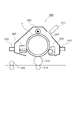
以下、電子写真感光体の好適な実施形態について詳述する。図1〜3はそれぞれ電子写真感光体の好適な実施形態を示す模式断面図である。図1,3に示す電子写真感光体は、電荷発生材料を含有する層(電荷発生層5)と電荷輸送材料を含有する層(電荷輸送層6)とに機能が分離された感光層3を備えるものである。また、図2は、電荷発生材料と電荷輸送材料とを同一の層(単層型感光層8)に含有するものである。
Hereinafter, preferred embodiments of the electrophotographic photoreceptor will be described in detail. 1 to 3 are schematic cross-sectional views each showing a preferred embodiment of an electrophotographic photosensitive member. The electrophotographic photosensitive member shown in FIGS. 1 and 3 includes a
図1に示す電子写真感光体1は、導電性支持体2上に下引き層4、電荷発生層5、電荷輸送層6が順次積層された構造を有する。また、図2に示す電子写真感光体1は、導電性支持体2上に下引き層4、単層型感光層8が順次積層された構造を有する。また、図3に示す電子写真感光体1は、導電性支持体2上に下引き層4、電荷発生層5、電荷輸送層6、保護層7が順次積層された構造を有する。
The
次に、図1を参照して、電子写真感光体1の各要素について詳述する。
Next, with reference to FIG. 1, each element of the
導電性支持体2としては、従来使用されている通常のものが使用可能である。導電性支持体2として、例えば、アルミニウム、ニッケル、クロム、ステンレス鋼等の金属類;アルミニウム、チタニウム、ニッケル、クロム、ステンレス鋼、金、バナジウム、酸化錫、酸化インジウム、ITO等の薄膜を設けたプラスチックフィルム等;導電性付与剤を塗布、又は含浸させた紙又はプラスチックフィルム等が使用できる。また、導電性支持体の形状は、ドラム状に限られず、シート状、プレート状としてもよい。
As the
導電性支持体2を金属パイプとした場合、表面は素管のままであってもよいし、事前に鏡面切削、エッチング、陽極酸化、粗切削、センタレス研削、サンドブラスト、ウエットホーニング等の処理が行われていてもよい。
In the case where the
導電性支持体2上には感光層3が配置されるが、感光層3のうち導電性支持体2上には下引き層4が配置される。
The
下引き層4は、導電性物質及び結着樹脂を含んで構成される。
The
導電性物質としては、例えば、アルミニウム、銅、ニッケル、銀等の金属粉体や、酸化アンチモン、酸化インジウム、酸化スズ、酸化亜鉛等の導電性金属酸化物、カーボンファイバ、カーボンブラック、グラファイト粉末等が挙げられる。 Examples of the conductive substance include metal powders such as aluminum, copper, nickel, and silver, conductive metal oxides such as antimony oxide, indium oxide, tin oxide, and zinc oxide, carbon fiber, carbon black, and graphite powder. Is mentioned.
導電性金属酸化物としては、粒径が0.5μm以下の微粒子が好ましく用いられる。ここで粒径とは、平均1次粒径を意味する。下引き層4はリーク耐性獲得のために適切な抵抗を得ることが必要であり、そのため金属酸化物微粒子としては102〜1011Ω・cm程度の粉体抵抗が必要である。中でも上記範囲の抵抗値を有する酸化錫、酸化チタン、酸化亜鉛等の金属酸化物微粒子を用いることが好ましい。なお、金属酸化物微粒子の抵抗値が、上記下限値未満であると十分なリーク耐性が得られ難くなる傾向があり、他方、上記上限値を超えると残留電位上昇を引き起こし易くなる傾向がある。
As the conductive metal oxide, fine particles having a particle size of 0.5 μm or less are preferably used. Here, the particle size means an average primary particle size. The
また、金属酸化物微粒子は2種以上混合して用いることもできる。さらに、金属酸化物微粒子へカップリング剤による表面処理を行うことで、粉体抵抗を制御することができる。 Moreover, 2 or more types of metal oxide fine particles can be mixed and used. Furthermore, the powder resistance can be controlled by subjecting the metal oxide fine particles to a surface treatment with a coupling agent.
カップリング剤としては、所望の感光体特性を得られるものであればいかなるものでも用いることができる。具体的なカップリング剤としては、例えば、ビニルトリメトキシシラン、γ−メタクリルオキシプロピル−トリス(β−メトキシエトキシ)シラン、β−(3,4−エポキシシクロヘキシル)エチルトリメトキシシラン、γ−グリシドキシプロピルトリメトキシシラン、ビニルトリアセトキシシラン、γ−メルカプトプロピルトリメトキシシラン、γ−アミノプロピルトリエトキシシラン、N−β−(アミノエチル)−γ−アミノプロピルトリメトキシシラン、N−β−(アミノエチル)−γ−アミノプロピルメチルメトキシシラン、N,N−ビス(β−ヒドロキシエチル)−γ−アミノプロピルトリエトキシシラン、γ−クロルプロピルトリメトキシシラン等のシランカップリング剤が挙げられるが、これらに限定されるものではない。また、これらのカップリング剤は、1種を単独で又は2種以上を混合して用いることもできる。 Any coupling agent can be used as long as it can obtain desired photoreceptor characteristics. Specific coupling agents include, for example, vinyltrimethoxysilane, γ-methacryloxypropyl-tris (β-methoxyethoxy) silane, β- (3,4-epoxycyclohexyl) ethyltrimethoxysilane, γ-glycid. Xylpropyltrimethoxysilane, vinyltriacetoxysilane, γ-mercaptopropyltrimethoxysilane, γ-aminopropyltriethoxysilane, N-β- (aminoethyl) -γ-aminopropyltrimethoxysilane, N-β- (amino Examples include silane coupling agents such as ethyl) -γ-aminopropylmethylmethoxysilane, N, N-bis (β-hydroxyethyl) -γ-aminopropyltriethoxysilane, and γ-chloropropyltrimethoxysilane. It is not limited to. Moreover, these coupling agents can also be used individually by 1 type or in mixture of 2 or more types.
表面処理方法は公知の方法であればいかなる方法でも使用可能であるが、乾式法又は湿式法を用いることができる。乾式法にて表面処理を施す場合には金属酸化物微粒子をせん断力の大きなミキサ等で攪拌しながら、直接或いは有機溶媒又は水に溶解させたカップリング剤を添加して、乾燥空気や窒素ガスとともに噴霧させることによって均一に処理される。添加又は噴霧する際には50℃以上の温度で行われることが好ましい。添加又は噴霧した後、さらに100℃以上で焼き付けを行うことができる。 As the surface treatment method, any known method can be used, but a dry method or a wet method can be used. When surface treatment is performed by a dry method, a metal oxide fine particle is agitated with a mixer having a large shearing force or the like, or a coupling agent dissolved in an organic solvent or water is added to dry air or nitrogen gas. It is processed uniformly by spraying together. The addition or spraying is preferably performed at a temperature of 50 ° C. or higher. After addition or spraying, baking can be performed at 100 ° C. or higher.
焼き付けは、所望の電子写真特性が得られる温度、時間であれば任意の範囲で実施できる。乾式法においては、金属酸化物微粒子のカップリング剤による表面処理前に金属酸化物微粒子を加熱乾燥して、表面吸着水を除去することができる。表面吸着水を処理前に除去することによって、金属酸化物微粒子表面に均一にカップリング剤を吸着させることができる。 Baking can be carried out in an arbitrary range as long as the temperature and the time at which desired electrophotographic characteristics are obtained. In the dry method, the surface adsorbed water can be removed by heating and drying the metal oxide fine particles before the surface treatment with the coupling agent of the metal oxide fine particles. By removing the surface adsorbed water before the treatment, the coupling agent can be uniformly adsorbed on the surface of the metal oxide fine particles.
湿式法としては、先ず、金属酸化物微粒子を溶剤中に攪拌、超音波、サンドミルやアトライター、ボールミル等を用いて分散する。次に、カップリング剤溶液を添加して攪拌又は分散したのち、溶剤除去することで均一に処理される。溶剤除去した後、さらに100℃以上で焼き付けを行うことができる。焼き付けは、所望の電子写真特性が得られる温度、時間であれば任意の範囲で実施できる。湿式法においても金属酸化物微粒子のカップリング剤による表面処理前に表面吸着水を除去することができる。この表面吸着水除去方法として、乾式法と同様の加熱乾燥の他に、表面処理に用いる溶剤中で攪拌加熱しながら除去する方法、溶剤と共沸させて除去する方法等が実施できる。 As a wet method, first, metal oxide fine particles are dispersed in a solvent by using stirring, ultrasonic waves, a sand mill, an attritor, a ball mill or the like. Next, after the coupling agent solution is added and stirred or dispersed, the solvent is removed to uniformly treat. After removing the solvent, baking can be performed at 100 ° C. or higher. Baking can be carried out in an arbitrary range as long as the temperature and the time at which desired electrophotographic characteristics are obtained. Even in the wet method, the surface adsorbed water can be removed before the surface treatment with the coupling agent of the metal oxide fine particles. As this surface adsorbed water removal method, in addition to heat drying similar to the dry method, a method of removing while stirring and heating in a solvent used for the surface treatment, a method of removing by azeotropy with the solvent, and the like can be carried out.
なお、金属酸化物微粒子に対する表面処理剤の量は、所望の電子写真特性が得られる量であることが必須である。電子写真特性は、表面処理後に金属酸化物微粒子に付着している表面処理剤の量に影響される。表面処理剤がシランカップリング剤の場合、その付着量は蛍光X線分析におけるSi強度と金属酸化物の主たる金属元素強度から求められる。蛍光X線分析における好ましいSi強度は、金属酸化物の主たる金属元素強度の1.0×10⁻⁵〜1.0×10⁻³の範囲である。Si強度が、上記下限値未満の場合にはかぶり等の画質欠陥が発生しやすくなる傾向があり、他方、上記上限値を超える場合には残留電位の上昇による濃度低下が発生しやすくなる傾向がある。 In addition, it is essential that the amount of the surface treatment agent with respect to the metal oxide fine particles is an amount capable of obtaining desired electrophotographic characteristics. The electrophotographic characteristics are affected by the amount of the surface treatment agent attached to the metal oxide fine particles after the surface treatment. When the surface treatment agent is a silane coupling agent, the amount of adhesion is determined from the Si intensity in the fluorescent X-ray analysis and the main metal element intensity of the metal oxide. The preferable Si intensity in the fluorescent X-ray analysis is in the range of 1.0 × 10 −5 to 1.0 × 10 −3 of the main metal element strength of the metal oxide. When the Si intensity is less than the above lower limit, image quality defects such as fog tend to occur. On the other hand, when the Si intensity exceeds the above upper limit, density tends to decrease due to an increase in residual potential. is there.
結着樹脂としては、ポリビニルブチラール等のアセタール樹脂、ポリビニルアルコール樹脂、カゼイン、ポリアミド樹脂、セルロース樹脂、ゼラチン、ポリウレタン樹脂、ポリエステル樹脂、メタクリル樹脂、アクリル樹脂、ポリ塩化ビニル樹脂、ポリビニルアセテート樹脂、塩化ビニル−酢酸ビニル−無水マレイン酸樹脂、シリコーン樹脂、シリコーン−アルキッド樹脂、フェノール樹脂、フェノール−ホルムアルデヒド樹脂、メラミン樹脂、ウレタン樹脂等の公知の高分子樹脂化合物、また電荷輸送性基を有する電荷輸送性樹脂やポリアニリン等の導電性樹脂等が挙げられる。中でも上層(電荷発生層5)の塗布溶剤に不溶な樹脂が好ましく用いられ、特にフェノール樹脂、フェノール−ホルムアルデヒド樹脂、メラミン樹脂、ウレタン樹脂、エポキシ樹脂等が好ましく用いられる。 Examples of the binder resin include acetal resins such as polyvinyl butyral, polyvinyl alcohol resin, casein, polyamide resin, cellulose resin, gelatin, polyurethane resin, polyester resin, methacrylic resin, acrylic resin, polyvinyl chloride resin, polyvinyl acetate resin, vinyl chloride. -Known polymer resin compounds such as vinyl acetate-maleic anhydride resin, silicone resin, silicone-alkyd resin, phenol resin, phenol-formaldehyde resin, melamine resin, urethane resin, and charge transport resin having a charge transport group And conductive resins such as polyaniline. Among these, resins insoluble in the coating solvent for the upper layer (charge generation layer 5) are preferably used, and phenol resins, phenol-formaldehyde resins, melamine resins, urethane resins, epoxy resins and the like are particularly preferably used.
下引き層4は、上記導電性物質を結着樹脂に分散して下引き層形成用塗布液を作製し、支持体上に塗布して形成される。下引き層形成用塗布液中の金属酸化物微粒子と結着樹脂との比率は、所望する電子写真特性を得られる範囲で任意に設定できる。
The
下引き層形成用塗布液には、電気特性向上、環境安定性向上、画質向上のために種々の添加物を用いることができる。添加物としては、クロラニル、ブロモアニル、アントラキノン等のキノン系化合物、テトラシアノキノジメタン系化合物、2,4,7−トリニトロフルオレノン、2,4,5,7−テトラニトロ−9−フルオレノン等のフルオレノン化合物、2−(4−ビフェニル)−5−(4−t−ブチルフェニル)−1,3,4−オキサジアゾールや2,5−ビス(4−ナフチル)−1,3,4−オキサジアゾール、2,5−ビス(4−ジエチルアミノフェニル)1,3,4オキサジアゾール等のオキサジアゾール系化合物、キサントン系化合物、チオフェン化合物、3,3’,5,5’テトラ−t−ブチルジフェノキノン等のジフェノキノン化合物等の電子輸送性物質、多環縮合系、アゾ系等の電子輸送性顔料、ジルコニウムキレート化合物、チタニウムキレート化合物、アルミニウムキレート化合物、チタニウムアルコキシド化合物、有機チタニウム化合物、シランカップリング剤等の公知の材料を用いることができる。シランカップリング剤は、金属酸化物微粒子の表面処理に用いられるが、添加剤としてさらに塗布液に添加して用いることもできる。 Various additives can be used in the coating liquid for forming the undercoat layer in order to improve electrical characteristics, environmental stability, and image quality. Additives include quinone compounds such as chloranil, bromoanil and anthraquinone, tetracyanoquinodimethane compounds, fluorenones such as 2,4,7-trinitrofluorenone and 2,4,5,7-tetranitro-9-fluorenone Compounds, 2- (4-biphenyl) -5- (4-t-butylphenyl) -1,3,4-oxadiazole and 2,5-bis (4-naphthyl) -1,3,4-oxadi Azoles, oxadiazole compounds such as 2,5-bis (4-diethylaminophenyl) 1,3,4 oxadiazole, xanthone compounds, thiophene compounds, 3,3 ′, 5,5 ′ tetra-t-butyl Electron transporting materials such as diphenoquinone compounds such as diphenoquinone, electron transporting pigments such as polycyclic condensation systems and azo systems, zirconium chelate compounds, titanium Chelate compounds, aluminum chelate compounds, titanium alkoxide compounds, organic titanium compounds, there can be used a known material such as a silane coupling agent. The silane coupling agent is used for the surface treatment of the metal oxide fine particles, but it can also be used as an additive added to the coating solution.
ここで用いられるシランカップリング剤としては、金属酸化物微粒子の表面処理に用いるカップリング剤と同様なものを用いることができる。 As a silane coupling agent used here, the thing similar to the coupling agent used for the surface treatment of metal oxide fine particles can be used.
ジルコニウムキレート化合物としては、ジルコニウムブトキシド、ジルコニウムアセト酢酸エチル、ジルコニウムトリエタノールアミン、アセチルアセトネートジルコニウムブトキシド、アセト酢酸エチルジルコニウムブトキシド、ジルコニウムアセテート、ジルコニウムオキサレート、ジルコニウムラクテート、ジルコニウムホスホネート、オクタン酸ジルコニウム、ナフテン酸ジルコニウム、ラウリン酸ジルコニウム、ステアリン酸ジルコニウム、イソステアリン酸ジルコニウム、メタクリレートジルコニウムブトキシド、ステアレートジルコニウムブトキシド、イソステアレートジルコニウムブトキシド等が挙げられる。 Zirconium chelate compounds include: zirconium butoxide, zirconium zirconium acetoacetate, zirconium triethanolamine, acetylacetonate zirconium butoxide, ethyl acetoacetate butoxide, zirconium acetate, zirconium oxalate, zirconium lactate, zirconium phosphonate, zirconium octoate, naphthenic acid Zirconium, zirconium laurate, zirconium stearate, zirconium isostearate, methacrylate zirconium butoxide, stearate zirconium butoxide, isostearate zirconium butoxide and the like.
チタニウムキレート化合物としては、テトライソプロピルチタネート、テトラノルマルブチルチタネート、ブチルチタネートダイマー、テトラ(2−エチルヘキシル)チタネート、チタンアセチルアセトネート、ポリチタンアセチルアセトネート、チタンオクチレングリコレート、チタンラクテートアンモニウム塩、チタンラクテート、チタンラクテートエチルエステル、チタントリエタノールアミネート、ポリヒドロキシチタンステアレート等が挙げられる。 Titanium chelate compounds include tetraisopropyl titanate, tetranormal butyl titanate, butyl titanate dimer, tetra (2-ethylhexyl) titanate, titanium acetylacetonate, polytitanium acetylacetonate, titanium octylene glycolate, titanium lactate ammonium salt, titanium Examples include lactate, titanium lactate ethyl ester, titanium triethanolamate, and polyhydroxytitanium stearate.
アルミニウムキレート化合物としては、アルミニウムイソプロピレート、モノブトキシアルミニウムジイソプロピレート、アルミニウムブチレート、ジエチルアセトアセテートアルミニウムジイソプロピレート、アルミニウムトリス(エチルアセトアセテート)等が挙げられる。 Examples of the aluminum chelate compound include aluminum isopropylate, monobutoxy aluminum diisopropylate, aluminum butyrate, diethyl acetoacetate aluminum diisopropylate, and aluminum tris (ethyl acetoacetate).
これらの化合物は、1種を単独で或いは複数の化合物の混合物又は重縮合物として用いることができる。 These compounds can be used alone or as a mixture or polycondensate of a plurality of compounds.
下引き層形成用塗布液に使用される溶媒としては、公知の有機溶剤、例えば、トルエン、クロロベンゼン等の芳香族炭化水素系溶剤、メタノール、エタノール、n−プロパノール、iso−プロパノール、n―ブタノール等の脂肪族アルコール系溶剤、アセトン、シクロヘキサノン、2−ブタノン等のケトン系溶剤、塩化メチレン、クロロホルム、塩化エチレン等のハロゲン化脂肪族炭化水素溶剤、テトラヒドロフラン、ジオキサン、エチレングリコール、ジエチルエーテル等の環状又は直鎖状エーテル系溶剤、酢酸メチル、酢酸エチル、酢酸n−ブチル等のエステル系溶剤が挙げられる。これらの溶剤は、1種を単独で又は2種以上を混合して用いることができる。混合する際、使用される溶剤としては、混合溶剤として結着樹脂を溶かすことができる溶剤であれば、いかなるものでも使用することが可能である。 Examples of the solvent used for the coating solution for forming the undercoat layer include known organic solvents such as aromatic hydrocarbon solvents such as toluene and chlorobenzene, methanol, ethanol, n-propanol, iso-propanol, n-butanol and the like. Aliphatic alcohol solvents, ketone solvents such as acetone, cyclohexanone and 2-butanone, halogenated aliphatic hydrocarbon solvents such as methylene chloride, chloroform and ethylene chloride, cyclic such as tetrahydrofuran, dioxane, ethylene glycol and diethyl ether or Examples include linear ether solvents, and ester solvents such as methyl acetate, ethyl acetate, and n-butyl acetate. These solvents can be used alone or in combination of two or more. When mixing, any solvent can be used as long as it can dissolve the binder resin as a mixed solvent.
また、金属酸化物微粒子を分散させる方法としては、ボールミル、振動ボールミル、アトライター、サンドミル、横型サンドミル等のメディア分散機や、攪拌、超音波分散機、ロールミル、高圧ホモジナイザー等のメディアレス分散機が利用できる。さらに、高圧ホモジナイザーとして、高圧状態で分散液を液−液衝突や液−壁衝突させて分散する衝突方式や、高圧状態で微細な流路を貫通させて分散する貫通方式等が挙げられる。 In addition, as a method for dispersing the metal oxide fine particles, there are a media disperser such as a ball mill, a vibrating ball mill, an attritor, a sand mill, a horizontal sand mill, and a medialess disperser such as an agitator, an ultrasonic disperser, a roll mill, and a high-pressure homogenizer. Available. Furthermore, examples of the high-pressure homogenizer include a collision method in which the dispersion liquid is dispersed by liquid-liquid collision or liquid-wall collision in a high pressure state, and a penetration method in which a fine flow path is dispersed in a high pressure state.
下引き層4を形成する際の塗布方法としては、浸漬塗布法、突き上げ塗布法、ワイヤーバー塗布法、スプレー塗布法、ブレード塗布法、ナイフ塗布法、カーテン塗布法等の通常の方法を用いることができる。
As a coating method for forming the
下引き層4は、ビッカース強度が35以上であることが好ましい。下引き層4の膜厚は、15μm以上であることが好ましく、20〜50μmであることがさらに好ましい。
The
また、下引き層4の表面粗さはモアレ像防止のために、使用される露光用レーザー波長λの1/4n(nは上層の屈折率)からλに調整される。表面粗さ調整のために下引き層4中に樹脂粒子を添加することもできる。樹脂粒子としてはシリコーン樹脂粒子、架橋型PMMA樹脂粒子等を用いることができる。
Further, the surface roughness of the
また、表面粗さ調整のために下引き層4を研磨することもできる。研磨方法としては、バフ研磨、サンドブラスト処理、ウエットホーニング、研削処理等を用いることもできる。
Further, the
さらに、この下引き層4と上層との間に、電気特性向上、画質向上、画質維持性向上、感光層接着性向上等のために中間層を設けてもよい。中間層に用いられる結着樹脂としては、ポリビニルブチラール等のアセタール樹脂、ポリビニルアルコール樹脂、カゼイン、ポリアミド樹脂、セルロース樹脂、ゼラチン、ポリウレタン樹脂、ポリエステル樹脂、メタクリル樹脂、アクリル樹脂、ポリ塩化ビニル樹脂、ポリビニルアセテート樹脂、塩化ビニル−酢酸ビニル−無水マレイン酸樹脂、シリコーン樹脂、シリコーン−アルキッド樹脂、フェノール−ホルムアルデヒド樹脂、メラミン樹脂等の高分子樹脂化合物のほかに、ジルコニウム、チタニウム、アルミニウム、マンガン、シリコン原子等を含有する有機金属化合物等が挙げられる。これらの化合物は、1種を単独で、或いは複数の化合物の混合物又は重縮合物として用いることができる。
Further, an intermediate layer may be provided between the
中でも、ジルコニウム又はシリコンを含有する有機金属化合物は残留電位が低く環境による電位変化が少なく、また繰り返し使用による電位の変化が少ない等性能上優れている。 Among these, organometallic compounds containing zirconium or silicon are excellent in performance, such as low residual potential, little potential change due to environment, and little potential change due to repeated use.
有機ジルコニウム化合物としては、ジルコニウムブトキシド、ジルコニウムアセト酢酸エチル、ジルコニウムトリエタノールアミン、アセチルアセトネートジルコニウムブトキシド、アセト酢酸エチルジルコニウムブトキシド、ジルコニウムアセテート、ジルコニウムオキサレート、ジルコニウムラクテート、ジルコニウムホスホネート、オクタン酸ジルコニウム、ナフテン酸ジルコニウム、ラウリン酸ジルコニウム、ステアリン酸ジルコニウム、イソステアリン酸ジルコニウム、メタクリレートジルコニウムブトキシド、ステアレートジルコニウムブトキシド、イソステアレートジルコニウムブトキシド等が挙げられる。 Examples of organic zirconium compounds include zirconium butoxide, zirconium zirconium acetoacetate, zirconium triethanolamine, acetylacetonate zirconium butoxide, ethyl acetoacetate butoxide, zirconium acetate, zirconium oxalate, zirconium lactate, zirconium phosphonate, zirconium octoate, naphthenic acid. Zirconium, zirconium laurate, zirconium stearate, zirconium isostearate, methacrylate zirconium butoxide, stearate zirconium butoxide, isostearate zirconium butoxide and the like.
有機シリコン化合物としては、ビニルトリメトキシシラン、γ−メタクリルオキシプロピル−トリス(β−メトキシエトキシ)シラン、β−(3,4−エポキシシクロヘキシル)エチルトリメトキシシラン、γ−グリシドキシプロピルトリメトキシシラン、ビニルトリアセトキシシラン、γ−メルカプトプロピルトリメトキシシラン、γ−アミノプロピルトリエトキシシラン、N−β−(アミノエチル)−γ−アミノプロピルトリメトキシシラン、N−β−(アミノエチル)−γ−アミノプロピルメチルメトキシシラン、N,N−ビス(β−ヒドロキシエチル)−γ−アミノプロピルトリエトキシシラン、γ−クロルプロピルトリメトキシシラン等が挙げられる。これらの中でも特に好ましく用いられるシリコン化合物は、ビニルトリエトキシシラン、ビニルトリス(2−メトキシエトキシシラン)、3−メタクリロキシプロピルトリメトキシシラン、3−グリシドキシプロピルトリメトキシシラン、2−(3,4−エポキシシクロヘキシル)エチルトリメトキシシラン、N−2−(アミノエチル)3−アミノプロピルトリメトキシシラン、N−2−(アミノエチル)3−アミノプロピルメチルジメトキシシラン、3−アミノプロピルトリエトキシシラン、N−フェニル−3−アミノプロピルトリメトキシシラン、3−メルカプトプロピルトリメトキシシラン、3−クロロプロピルトリメトキシシラン等のシランカップリング剤が挙げられる。 As organic silicon compounds, vinyltrimethoxysilane, γ-methacryloxypropyl-tris (β-methoxyethoxy) silane, β- (3,4-epoxycyclohexyl) ethyltrimethoxysilane, γ-glycidoxypropyltrimethoxysilane , Vinyltriacetoxysilane, γ-mercaptopropyltrimethoxysilane, γ-aminopropyltriethoxysilane, N-β- (aminoethyl) -γ-aminopropyltrimethoxysilane, N-β- (aminoethyl) -γ- Examples include aminopropylmethylmethoxysilane, N, N-bis (β-hydroxyethyl) -γ-aminopropyltriethoxysilane, and γ-chloropropyltrimethoxysilane. Among these, particularly preferable silicon compounds are vinyltriethoxysilane, vinyltris (2-methoxyethoxysilane), 3-methacryloxypropyltrimethoxysilane, 3-glycidoxypropyltrimethoxysilane, 2- (3,4 -Epoxycyclohexyl) ethyltrimethoxysilane, N-2- (aminoethyl) 3-aminopropyltrimethoxysilane, N-2- (aminoethyl) 3-aminopropylmethyldimethoxysilane, 3-aminopropyltriethoxysilane, N Examples include silane coupling agents such as phenyl-3-aminopropyltrimethoxysilane, 3-mercaptopropyltrimethoxysilane, and 3-chloropropyltrimethoxysilane.
有機チタン化合物としては、テトライソプロピルチタネート、テトラノルマルブチルチタネート、ブチルチタネートダイマー、テトラ(2−エチルヘキシル)チタネート、チタンアセチルアセトネート、ポリチタンアセチルアセトネート、チタンオクチレングリコレート、チタンラクテートアンモニウム塩、チタンラクテート、チタンラクテートエチルエステル、チタントリエタノールアミネート、ポリヒドロキシチタンステアレート等が挙げられる。 Examples of organic titanium compounds include tetraisopropyl titanate, tetranormal butyl titanate, butyl titanate dimer, tetra (2-ethylhexyl) titanate, titanium acetylacetonate, polytitanium acetylacetonate, titanium octylene glycolate, titanium lactate ammonium salt, titanium Examples include lactate, titanium lactate ethyl ester, titanium triethanolamate, and polyhydroxytitanium stearate.
有機アルミニウム化合物としては、アルミニウムイソプロピレート、モノブトキシアルミニウムジイソプロピレート、アルミニウムブチレート、ジエチルアセトアセテートアルミニウムジイソプロピレート、アルミニウムトリス(エチルアセトアセテート)等が挙げられる。 Examples of the organoaluminum compound include aluminum isopropylate, monobutoxyaluminum diisopropylate, aluminum butyrate, diethyl acetoacetate aluminum diisopropylate, and aluminum tris (ethyl acetoacetate).
中間層の形成に使用される溶媒としては、公知の有機溶剤、例えば、トルエン、クロロベンゼン等の芳香族炭化水素系溶剤、メタノール、エタノール、n−プロパノール、iso−プロパノール、n−ブタノール等の脂肪族アルコール系溶剤、アセトン、シクロヘキサノン、2−ブタノン等のケトン系溶剤、塩化メチレン、クロロホルム、塩化エチレン等のハロゲン化脂肪族炭化水素溶剤、テトラヒドロフラン、ジオキサン、エチレングリコール、ジエチルエーテル等の環状又は直鎖状エーテル系溶剤、酢酸メチル、酢酸エチル、酢酸n−ブチル等のエステル系溶剤が挙げられる。これらの溶剤は、1種を単独で又は2種以上を混合して用いることができる。混合する際、使用される溶剤としては、混合溶剤として結着樹脂を溶かすことができる溶剤であれば、いかなるものでも使用することが可能である。 As the solvent used for forming the intermediate layer, known organic solvents, for example, aromatic hydrocarbon solvents such as toluene and chlorobenzene, aliphatics such as methanol, ethanol, n-propanol, iso-propanol, and n-butanol Alcohol solvents, ketone solvents such as acetone, cyclohexanone and 2-butanone, halogenated aliphatic hydrocarbon solvents such as methylene chloride, chloroform and ethylene chloride, cyclic or straight chain such as tetrahydrofuran, dioxane, ethylene glycol and diethyl ether Examples include ether solvents, ester solvents such as methyl acetate, ethyl acetate, and n-butyl acetate. These solvents can be used alone or in combination of two or more. When mixing, any solvent can be used as long as it can dissolve the binder resin as a mixed solvent.
中間層を形成する際の塗布方法としては、浸漬塗布法、突き上げ塗布法、ワイヤーバー塗布法、スプレー塗布法、ブレード塗布法、ナイフ塗布法、カーテン塗布法等の通常の方法を用いることができる。 As a coating method for forming the intermediate layer, a usual method such as a dip coating method, a push-up coating method, a wire bar coating method, a spray coating method, a blade coating method, a knife coating method, or a curtain coating method can be used. .
中間層は上層の塗布性改善の他に、電気的なブロッキング層の役割も果たすが、膜厚が大きすぎる場合には電気的な障壁が強くなりすぎて減感や繰り返しによる電位の上昇を引き起こし易くなる傾向がある。したがって、中間層の膜厚は、0.1〜3μmが好ましい。また、この場合の中間層を併せて、下引き層4として使用してもよい。
In addition to improving the coatability of the upper layer, the intermediate layer also serves as an electrical blocking layer.However, if the film thickness is too large, the electrical barrier becomes too strong, causing desensitization and potential increase due to repetition. It tends to be easier. Therefore, the film thickness of the intermediate layer is preferably 0.1 to 3 μm. Further, the intermediate layer in this case may be used together as the
下引き層4上には、電荷発生層5が配置される。電荷発生層5は、電荷発生材料を含んで構成される。
On the
電荷発生材料としては、例えば、無金属フタロシアニン、オキシチタニウムフタロシアニン、クロロガリウムフタロシアニン、ヒドロキシガリウムフタロシアニン、ジクロロスズフタロシアニン、チタニルフタロシアニン等のフタロシアニン顔料が使用可能である。その他、電荷発生材料としては、キノン顔料、ペリレン顔料、インジゴ顔料、ビスベンゾイミダゾール顔料、アントロン顔料、キナクリドン顔料、フタロシアニン顔料等を使用することができる。また、これらの電荷発生材料は、単独又は2種以上を混合して使用することができる。これらの中では、無金属フタロシアニン、オキシチタニウムフタロシアニン、クロロガリウムフタロシアニン、ヒドロキシガリウムフタロシアニン、ジクロロスズフタロシアニン、及びチタニルフタロシアニンから選ばれる少なくとも1種が好ましい。 As the charge generation material, for example, phthalocyanine pigments such as metal-free phthalocyanine, oxytitanium phthalocyanine, chlorogallium phthalocyanine, hydroxygallium phthalocyanine, dichlorotin phthalocyanine, and titanyl phthalocyanine can be used. In addition, quinone pigments, perylene pigments, indigo pigments, bisbenzimidazole pigments, anthrone pigments, quinacridone pigments, phthalocyanine pigments, and the like can be used as charge generation materials. Moreover, these charge generation materials can be used individually or in mixture of 2 or more types. Among these, at least one selected from metal-free phthalocyanine, oxytitanium phthalocyanine, chlorogallium phthalocyanine, hydroxygallium phthalocyanine, dichlorotin phthalocyanine, and titanyl phthalocyanine is preferable.
特に、CuKα特性X線に対するブラッグ角(2θ±0.2゜)の少なくとも7.7゜、9.3゜、16.9゜、17.5゜、22.4゜及び28.8゜に強い回折ピークを有する無金属フタロシアニン結晶、CuKα特性X線に対するブラッグ角(2θ±0.2゜)の少なくとも7.4゜、16.6゜、25.5゜及び28.3゜に強い回折ピークを有するクロロガリウムフタロシアニン結晶、CuKα特性X線に対するブラッグ角(2θ±0.2゜)の少なくとも7.5゜、9.9゜、12.5゜、16.3゜、18.6゜、25.1゜及び28.3゜に強い回折ピークを有するヒドロキシガリウムフタロシアニン結晶、並びにCuKα特性X線に対するブラッグ角(2θ±0.2゜)の少なくとも9.6゜、24.1゜及び27.2゜に強い回折ピークを有するチタニルフタロシアニン結晶から選ばれる少なくとも1種が好ましい。 In particular, it is strong at least 7.7 °, 9.3 °, 16.9 °, 17.5 °, 22.4 ° and 28.8 ° of the Bragg angle (2θ ± 0.2 °) with respect to CuKα characteristic X-rays. Metal-free phthalocyanine crystals having diffraction peaks, strong diffraction peaks at Bragg angles (2θ ± 0.2 °) of CuKα characteristic X-rays of at least 7.4 °, 16.6 °, 25.5 ° and 28.3 ° A chlorogallium phthalocyanine crystal having CuKα characteristic X-ray with a Bragg angle (2θ ± 0.2 °) of at least 7.5 °, 9.9 °, 12.5 °, 16.3 °, 18.6 °, 25. Hydroxygallium phthalocyanine crystals with strong diffraction peaks at 1 ° and 28.3 °, and at least 9.6 °, 24.1 ° and 27.2 ° Bragg angles (2θ ± 0.2 °) with respect to CuKα characteristic X-rays Strong times At least one selected from titanyl phthalocyanine crystal having a peak is preferred.
さらに、クロロガリウムフタロシアニン結晶としては、CuKαを線源とするX線回折スペクトルにおいて、ブラッグ角度(2θ±0.2°)の7.4°、16.6°、25.5°、28.3°に強い回折ピークを有するクロロガリウムフタロシアニン結晶(I−1)、ブラッグ角度(2θ±0.2°)の6.8°、17.3°、23.6°、26.9°に強い回折ピークを有するクロロガリウムフタロシアニン結晶(I−2)、及びブラッグ角度(2θ±0.2°)の8.7°〜9.2°、17.6°、24.0°、27.4°、28.8°に強い回折ピークを有するクロロガリウムフタロシアニン結晶(I−3)が好ましい。 Furthermore, as a chlorogallium phthalocyanine crystal, in an X-ray diffraction spectrum using CuKα as a radiation source, 7.4 °, 16.6 °, 25.5 °, 28.3 of Bragg angles (2θ ± 0.2 °) are used. Chlorogallium phthalocyanine crystal (I-1) having a strong diffraction peak at °, strong diffraction at 6.8 °, 17.3 °, 23.6 ° and 26.9 ° of Bragg angle (2θ ± 0.2 °) Chlorogallium phthalocyanine crystal having a peak (I-2) and Bragg angles (2θ ± 0.2 °) of 8.7 ° to 9.2 °, 17.6 °, 24.0 °, 27.4 °, Chlorogallium phthalocyanine crystal (I-3) having a strong diffraction peak at 28.8 ° is preferred.
ジクロロスズフタロシアニン結晶としては、CuKαを線源とするX線回折スペクトルにおいて、ブラッグ角度(2θ±0.2°)の8.3°、12.2°、13.7°、15.9°、18.9°、28.2°に強い回折ピークを有するジクロロスズフタロシアニン結晶(I−4)、ブラッグ角度(2θ±0.2°)の8.5°、11.2°、14.5°、27.2°に強い回折ピークを有するジクロロスズフタロシアニン結晶(I−5)、ブラッグ角度(2θ±0.2°)の8.7°、9.9°、10.9°、13.1°、15.2°、16.3°、17.4°、21.9°、25.5°に強い回折ピークを有するジクロロスズフタロシアニン結晶(I−6)、及びブラッグ角度(2θ±0.2°)の9.2°、12.2°、13.4°、14.6°、17.0°、25.3°に強い回折ピークを有するジクロロスズフタロシアニン結晶(I−7)が好ましい。 As the dichlorotin phthalocyanine crystal, in the X-ray diffraction spectrum using CuKα as a radiation source, Bragg angles (2θ ± 0.2 °) of 8.3 °, 12.2 °, 13.7 °, 15.9 °, Dichlorotin phthalocyanine crystal (I-4) having a strong diffraction peak at 18.9 °, 28.2 °, Bragg angle (2θ ± 0.2 °) of 8.5 °, 11.2 °, 14.5 ° Dichlorotin phthalocyanine crystal (I-5) having a strong diffraction peak at 27.2 °, 8.7 °, 9.9 °, 10.9 °, 13.1 of Bragg angle (2θ ± 0.2 °) Dichlorotin phthalocyanine crystal (I-6) having strong diffraction peaks at °, 15.2 °, 16.3 °, 17.4 °, 21.9 °, 25.5 °, and Bragg angle (2θ ± 0. 9.2 °, 12.2 °, 13.4 °, 14.6 °, 17.0 °, Dichlorotin phthalocyanine crystal having strong diffraction peaks at 5.3 ° (I-7) are preferred.
ヒドロキシガリウムフタロシアニン結晶としては、CuKαを線源とするX線回折スペクトルにおいて、ブラッグ角度(2θ±0.2°)の7.7°、16.5°、25.1°、26.6°に強い回折ピークを有するヒドロキシガリウムフタロシアニン結晶(I−8)、ブラッグ角度(2θ±0.2°)の7.9°、16.5°、24.4°、27.6°に強い回折ピークを有するヒドロキシガリウムフタロシアニン結晶(I−9)、ブラッグ角度(2θ±0.2°)の7.0°、7.5°、10.5°、11.7°、12.7°、17.3°、18.1°、24.5°、26.2°、27.1°に強い回折ピークを有するヒドロキシガリウムフタロシアニン結晶(I−10)、ブラッグ角度(2θ±0.2°)の7.5°、9.9°、12.5°、16.3°、18.6°、25.1°、28.3°に強い回折ピークを有するヒドロキシガリウムフタロシアニン結晶(I−11)、及びブラッグ角度(2θ±0.2°)の6.8°、12.8°、15.8°、26.0°に強い回折ピークを有するヒドロキシガリウムフタロシアニン結晶(I−12)が好ましい。 The hydroxygallium phthalocyanine crystal has a Bragg angle (2θ ± 0.2 °) of 7.7 °, 16.5 °, 25.1 °, and 26.6 ° in an X-ray diffraction spectrum using CuKα as a radiation source. Hydroxygallium phthalocyanine crystal (I-8) having a strong diffraction peak, strong diffraction peaks at 7.9 °, 16.5 °, 24.4 ° and 27.6 ° of the Bragg angle (2θ ± 0.2 °) Having hydroxygallium phthalocyanine crystal (I-9), Bragg angle (2θ ± 0.2 °) of 7.0 °, 7.5 °, 10.5 °, 11.7 °, 12.7 °, 17.3 7. Hydroxygallium phthalocyanine crystal (I-10) having strong diffraction peaks at °, 18.1 °, 24.5 °, 26.2 °, 27.1 °, 7. Bragg angle (2θ ± 0.2 °). 5 °, 9.9 °, 12.5 °, 16.3 °, 18 Hydroxygallium phthalocyanine crystal (I-11) having strong diffraction peaks at .6 °, 25.1 °, and 28.3 °, and 6.8 ° and 12.8 ° of Bragg angle (2θ ± 0.2 °) , Hydroxygallium phthalocyanine crystals (I-12) having strong diffraction peaks at 15.8 ° and 26.0 ° are preferable.
無金属フタロシアニン結晶としては、X型無金属フタロシアニン結晶(I−13)が好ましい。 As the metal-free phthalocyanine crystal, X-type metal-free phthalocyanine crystal (I-13) is preferable.
オキシチタニウムフタロシアニン結晶としては、CuKαを線源とするX線回折スペクトルにおいて、ブラッグ角度(2θ±0.2°)の9.3°、10.6°、13.2°、15.1°、15.7°、16.1°、20.8°、23.3°、26.3°に強い回折ピークを有するオキシチタニウムフタロシアニン結晶(I−14)、ブラッグ角度(2θ±0.2°)の7.6°、10.2°、12.6°、13.2°、15.1°、16.3°、17.3°、18.3°、22.5°、24.2°、25.3°、28.6°に強い回折ピークを有するオキシチタニウムフタロシアニン結晶(I−15)及びブラッグ角度(2θ±0.2°)の9.7°、11.7°、15.0°、23.5°、27.3°に強い回折ピークを有するオキシチタニウムフタロシアニン結晶(I−16)が好ましい。上記フタロシアニン結晶((I−1)〜(I−16))のイオン化ポテンシャルの値を表1に示す。
As an oxytitanium phthalocyanine crystal, in an X-ray diffraction spectrum using CuKα as a radiation source, a Bragg angle (2θ ± 0.2 °) of 9.3 °, 10.6 °, 13.2 °, 15.1 °, Oxytitanium phthalocyanine crystal (I-14) having strong diffraction peaks at 15.7 °, 16.1 °, 20.8 °, 23.3 °, 26.3 °, Bragg angle (2θ ± 0.2 °) 7.6 °, 10.2 °, 12.6 °, 13.2 °, 15.1 °, 16.3 °, 17.3 °, 18.3 °, 22.5 °, 24.2 ° Oxytitanium phthalocyanine crystal (I-15) having strong diffraction peaks at 25.3 °, 28.6 °, and 9.7 °, 11.7 °, 15.0 of Bragg angle (2θ ± 0.2 °) Oxytitanium phthalocyanine crystals with strong diffraction peaks at 23.5 ° and 27.3 ° (I-16) are preferred. Table 1 shows the ionization potential values of the phthalocyanine crystals ((I-1) to (I-16)).

イオン化ポテンシャル測定装置:理研計器(株)製、表面分析装置AC−1(この装置は、大気中において、紫外線励起による光電子を計数し、サンプル表面を分析するもので、低エネルギー電子計数装置を用いたものである。)、
測定時の環境温度:20℃、
測定時の相対湿度:60%、
計数時間:10秒/1ポイント、
光量設定:50μW/cm2、
光量補正:上記設定で付属プログラムにより補正、
エネルギー走査範囲:3.4〜6.2eV、
紫外線スポット径:1mmSQ、
単位光量子:1×10¹⁰個/cm2・秒。
Ionization potential measurement device: Riken Keiki Co., Ltd., surface analysis device AC-1 (this device counts photoelectrons by ultraviolet excitation in the atmosphere and analyzes the sample surface, and uses a low energy electron counting device. ),
Environmental temperature during measurement: 20 ° C
Relative humidity during measurement: 60%
Counting time: 10 seconds / 1 point
Light intensity setting: 50 μW / cm 2
Light intensity correction: Corrected by the attached program with the above settings,
Energy scanning range: 3.4 to 6.2 eV,
UV spot diameter: 1mm SQ,
Unit photon: 1 × 10 10 / cm 2 · sec.
イオン化ポテンシャルの測定の際に測定サンプルは、深さ1mm、直径7mmのアルミニウム製のパンに、測定試料の粉末を入れ、測定試料の粉末表面と紫外線照射位置との距離が2mmとなるように設定する。 When measuring the ionization potential, the measurement sample is set so that the distance between the powder surface of the measurement sample and the ultraviolet irradiation position is 2 mm in an aluminum pan having a depth of 1 mm and a diameter of 7 mm. To do.
そして、イオン化ポテンシャルは、装置に付属している仕事関数算出プログラムに従い、縦軸を計数値(CPS)の平方根、横軸を紫外線励起エネルギー(eV)として得られる曲線における、バックグラウンドに対応する直線部分を外挿した直線と、計数値が急激に上昇した箇所に対応する直線部分を外挿した直線との交点により求められる。 The ionization potential is a straight line corresponding to the background in a curve obtained with the square root of the count value (CPS) on the vertical axis and the ultraviolet excitation energy (eV) on the horizontal axis according to the work function calculation program attached to the apparatus. It is obtained by the intersection of a straight line obtained by extrapolating the part and a straight line obtained by extrapolating the straight line part corresponding to the place where the count value has rapidly increased.
図4は、上記イオン化ポテンシャル測定装置によって測定される計数値(CPS)の平方根と紫外線励起エネルギー(eV)との関係の一例を示す曲線である。以下に、図4に示した曲線からイオン化ポテンシャルIpを求める方法について説明する。図4中、曲線10は、測定されたCPSの平方根と紫外線励起エネルギーとの関係を示している。曲線10には、バックグラウンドに対応する直線部分12と、紫外線励起エネルギーの増加に伴い徐々に計数値が上昇し、さらなる紫外線励起エネルギーの増加により計数値が急激に上昇した箇所に対応する直線部分11とがある。図4において、イオン化ポテンシャルIPは、直線部分12と11とを外挿し、その外挿線(破線)の交点13の横軸(紫外線励起エネルギー軸)上の値(eV)である。
FIG. 4 is a curve showing an example of the relationship between the square root of the count value (CPS) measured by the ionization potential measuring apparatus and the ultraviolet excitation energy (eV). Hereinafter, a method for obtaining the ionization potential Ip from the curve shown in FIG. 4 will be described. In FIG. 4, a
電荷発生層5は、例えば、結着樹脂中に電荷発生材料を分散して電荷発生層形成用塗布液を作製し、その塗布液を下引き層4上に塗布して形成することができる。
The
結着樹脂としては、例えば、ビスフェノールAタイプ又はビスフェノールZタイプ等のポリカーボネート樹脂、アクリル樹脂、メタクリル樹脂、ポリアリレート樹脂、ポリエステル樹脂、ポリ塩化ビニル樹脂、ポリスチレン樹脂、アクリロニトリル−スチレン共重合体樹脂、アクリロニトリル−ブタジエン共重合体、ポリビニルアセテート樹脂、ポリビニルホルマール樹脂、ポリスルホン樹脂、スチレン−ブタジエン共重合体樹脂、塩化ビニリデン−アクリルニトリル共重合体樹脂、塩化ビニル−酢酸ビニル−無水マレイン酸樹脂、シリコーン樹脂、フェノール−ホルムアルデヒド樹脂、ポリアクリルアミド樹脂、ポリアミド樹脂、ポリ−N−ビニルカルバゾール樹脂等を用いることができる。これらの結着樹脂は、1種を単独で又は2種以上混合して用いることが可能である。 Examples of the binder resin include polycarbonate resin such as bisphenol A type or bisphenol Z type, acrylic resin, methacrylic resin, polyarylate resin, polyester resin, polyvinyl chloride resin, polystyrene resin, acrylonitrile-styrene copolymer resin, acrylonitrile. -Butadiene copolymer, polyvinyl acetate resin, polyvinyl formal resin, polysulfone resin, styrene-butadiene copolymer resin, vinylidene chloride-acrylonitrile copolymer resin, vinyl chloride-vinyl acetate-maleic anhydride resin, silicone resin, phenol -Formaldehyde resin, polyacrylamide resin, polyamide resin, poly-N-vinylcarbazole resin and the like can be used. These binder resins can be used singly or in combination of two or more.
電荷発生層形成用塗布液における、電荷発生材料と結着樹脂の配合比は、10:1〜1:10が望ましい。 The mixing ratio of the charge generation material and the binder resin in the charge generation layer forming coating solution is preferably 10: 1 to 1:10.
電荷発生材料の分散に使用される溶剤としては、公知の有機溶剤、例えば、トルエン、クロロベンゼン等の芳香族炭化水素系溶剤、メタノール、エタノール、n−プロパノール、iso−プロパノール、n−ブタノール等の脂肪族アルコール系溶剤、アセトン、シクロヘキサノン、2−ブタノン等のケトン系溶剤、塩化メチレン、クロロホルム、塩化エチレン等のハロゲン化脂肪族炭化水素溶剤、テトラヒドロフラン、ジオキサン、エチレングリコール、ジエチルエーテル等の環状又は直鎖状エーテル系溶剤、酢酸メチル、酢酸エチル、酢酸n−ブチル等のエステル系溶剤が挙げられる。これらの溶剤は、1種を単独で又は2種以上を混合して用いることができる。混合する際、使用される溶剤としては、混合溶剤として結着樹脂を溶かすことができる溶剤であれば、いかなるものでも使用することが可能である。 Solvents used for dispersion of the charge generating material include known organic solvents such as aromatic hydrocarbon solvents such as toluene and chlorobenzene, fats such as methanol, ethanol, n-propanol, iso-propanol, and n-butanol. Aromatic alcohol solvents, ketone solvents such as acetone, cyclohexanone and 2-butanone, halogenated aliphatic hydrocarbon solvents such as methylene chloride, chloroform and ethylene chloride, cyclic or straight chain such as tetrahydrofuran, dioxane, ethylene glycol and diethyl ether And ether solvents such as methyl ether solvent, methyl acetate, ethyl acetate and n-butyl acetate. These solvents can be used alone or in combination of two or more. When mixing, any solvent can be used as long as it can dissolve the binder resin as a mixed solvent.
電荷発生材料を樹脂中に分散させる方法としては、ボールミル、振動ボールミル、アトライター、サンドミル、横型サンドミル等のメディア分散機や、攪拌、超音波分散機、ロールミル、高圧ホモジナイザー等のメディアレス分散機が利用できる。さらに、高圧ホモジナイザーとして、高圧状態で分散液を液−液衝突や液−壁衝突させて分散する衝突方式や、高圧状態で微細な流路を貫通させて分散する貫通方式等が挙げられる。 Examples of the method for dispersing the charge generating material in the resin include a media dispersing machine such as a ball mill, a vibrating ball mill, an attritor, a sand mill, and a horizontal sand mill, and a medialess dispersing machine such as an agitator, an ultrasonic dispersing machine, a roll mill, and a high-pressure homogenizer. Available. Furthermore, examples of the high-pressure homogenizer include a collision method in which the dispersion liquid is dispersed by liquid-liquid collision or liquid-wall collision in a high pressure state, and a penetration method in which a fine flow path is dispersed in a high pressure state.
電荷発生層5を形成する塗布方法としては、浸漬塗布法、突き上げ塗布法、ワイヤーバー塗布法、スプレー塗布法、ブレード塗布法、ナイフ塗布法、カーテン塗布法等の通常の方法を用いることができる。
As a coating method for forming the
電荷発生層5の膜厚は、好ましくは0.01〜5μm、より好ましくは0.05〜2.0μmの範囲に設定される。
The film thickness of the
電荷発生層5上、すなわち導電性支持体2から最も遠い側に電荷輸送層6が配置される。電荷輸送層6は、1種又は2種以上の電荷輸送材料と、フッ素系樹脂粒子と、フッ素系グラフトポリマーとを含有して構成される。
A
電荷輸送材料として、具体的には、トリアリールアミン系化合物、ベンジジン系化合物、アリールアルカン系化合物、アリール置換エチレン系化合物、スチルベン系化合物、アントラセン系化合物、ヒドラゾン系化合物、これらの化合物からなる基を主鎖又は側鎖に有する重合体等が挙げられる。これら電荷輸送材料は、1種を単独で又は2種以上を混合して用いてもよい。 Specific examples of charge transport materials include triarylamine compounds, benzidine compounds, arylalkane compounds, aryl-substituted ethylene compounds, stilbene compounds, anthracene compounds, hydrazone compounds, and groups composed of these compounds. Examples thereof include a polymer having a main chain or a side chain. These charge transport materials may be used alone or in combination of two or more.
これらの電荷輸送材料の中でも、ベンジジン系化合物、トリアリールアミン系化合物、及びこれらの化合物の混合物が好ましく使用される。ここで、トリアリールアミン系化合物の具体例をイオン化ポテンシャルの値とともに表2に、ベンジジン化合物の具体例をイオン化ポテンシャルの値と共に表3に示す。なお、イオン化ポテンシャルの測定は、上述した方法と同様の方法で行うことができる。 Among these charge transport materials, benzidine compounds, triarylamine compounds, and mixtures of these compounds are preferably used. Here, specific examples of triarylamine compounds are shown in Table 2 together with ionization potential values, and specific examples of benzidine compounds are shown in Table 3 together with ionization potential values. The ionization potential can be measured by the same method as described above.
フッ素系樹脂微粒子は、フッ素系樹脂を含む微粒子である。ここで、フッ素系樹脂とはフッ素原子を含有する樹脂であり、例えば、4フッ化エチレン樹脂、3フッ化塩化エチレン樹脂、6フッ化プロピレン樹脂、フッ化ビニル樹脂、フッ化ビニリデン樹脂、2フッ化2塩化エチレン樹脂及びこれらの共重合体が挙げられ、これらの中から1種を単独で又は2種以上を適宜選択して使用することが望ましい。上記の中でも特に、4フッ化エチレン樹脂、フッ化ビニリデン樹脂が好ましい。 The fluorine resin fine particles are fine particles containing a fluorine resin. Here, the fluorine-based resin is a resin containing a fluorine atom. For example, a tetrafluoroethylene resin, a trifluorinated ethylene resin, a hexafluoropropylene resin, a vinyl fluoride resin, a vinylidene fluoride resin, a two fluorine resin. Among these, it is desirable to use one of them alone or two or more appropriately selected from these. Of these, tetrafluoroethylene resin and vinylidene fluoride resin are particularly preferable.
フッ素系樹脂粒子の一次粒径は、0.05〜1μmが好ましく、0.1〜0.5μmがより好ましい。一次粒径が0.05μm未満であると、分散時に凝集し易くなる傾向があり、他方、1μmを超えると画質欠陥が発生し易くなる傾向がある。 The primary particle size of the fluororesin particles is preferably 0.05 to 1 μm, more preferably 0.1 to 0.5 μm. When the primary particle size is less than 0.05 μm, the particles tend to aggregate at the time of dispersion. On the other hand, when the particle size exceeds 1 μm, image quality defects tend to occur.
フッ素系グラフトポリマーとは、フッ素原子を含有するグラフトポリマーである。フッ素系グラフトポリマーは、塗布液の分散安定性を向上させ、塗膜形成時の凝集を防止する効果を有している。 The fluorine-based graft polymer is a graft polymer containing a fluorine atom. The fluorine-based graft polymer has an effect of improving the dispersion stability of the coating solution and preventing aggregation during the formation of the coating film.
フッ素系グラフトポリマーは、各分子鎖の片末端に重合性の官能基を有する分子量が1000〜10000の比較的低分子量のオリゴマーであるマクロモノマーと、フッ素系重合性モノマーを共重合して得られるものであり、フッ素系重合体を主鎖にもち、マクロモノマー重合体を枝にもつ構造を有している。 The fluorine-based graft polymer is obtained by copolymerizing a macromonomer, which is a relatively low molecular weight oligomer having a molecular weight of 1000 to 10,000, having a polymerizable functional group at one end of each molecular chain, and a fluorine-based polymerizable monomer. It has a structure in which the main chain is a fluoropolymer and the macromonomer polymer is in a branch.
マクロモノマーとしては、グラフトポリマーを添加する樹脂に親和性のあるものが選択され、例えば、アクリル酸エステル類、メタクリル酸エステル類、スチレン化合物等を単量体単位として含む重合体や共重合体等が挙げられる。また、フッ素系重合体としては、フッ素原子を分子内に有する重合性モノマー(フッ素系重合性モノマー)を単量体単位として含む重合体である。フッ素原子を分子内に有する重合性モノマーとしては、例えば、下記式(IV−1)〜(IV−6)に示されるものが挙げられる。これらは1種を単独で、又は2種以上を選択して、使用することができる。 As the macromonomer, those having an affinity for the resin to which the graft polymer is added are selected. For example, polymers and copolymers containing acrylic acid esters, methacrylic acid esters, styrene compounds as monomer units, etc. Is mentioned. Moreover, as a fluorine-type polymer, it is a polymer containing the polymerizable monomer (fluorine-type polymerizable monomer) which has a fluorine atom in a molecule | numerator as a monomer unit. As a polymerizable monomer which has a fluorine atom in a molecule | numerator, what is shown by following formula (IV-1)-(IV-6) is mentioned, for example. These can be used alone or in combination of two or more.
フッ素系グラフトポリマー中におけるフッ素系重合体の含有量は、フッ素系グラフトポリマー中5〜90重量%が好ましく、10〜70重量%が更に好ましい。フッ素系重合体の含有量が5重量%未満であると疎水化の改質効果が不十分となる傾向があり、他方、90重量%を越えると重合を行う際にマクロモノマーとの相溶性が悪くなる傾向がある。 The content of the fluorinated polymer in the fluorinated graft polymer is preferably from 5 to 90% by weight, more preferably from 10 to 70% by weight, based on the fluorinated graft polymer. If the content of the fluoropolymer is less than 5% by weight, the modification effect of hydrophobization tends to be insufficient. On the other hand, if the content exceeds 90% by weight, compatibility with the macromonomer is caused during polymerization. Tend to get worse.
電荷輸送層6における、1種又は2種以上の電荷輸送材料と、フッ素系樹脂粒子と、フッ素系グラフトポリマーとの種類及び含有量は、上記式(1)の条件を満たすように調節される。そして、図1に示す感光体1では、電荷輸送層6の電荷輸送性が特に優れたものとなるだけでなく、電荷発生層5から電荷輸送層6へ電荷が注入して電荷輸送層中を電荷が移動するに際して電荷発生材料と電荷輸送材料のマッチングに関わる電荷注入性をも特に優れたものとなると考えられる。
The type and content of one or more charge transport materials, fluorine resin particles, and fluorine graft polymer in the
フッ素系樹脂粒子の含有量は、上記式(1)の条件を満たせば特に制限されないが、電荷輸送層6全量に対し、0.1〜40wt%が好ましく、1〜30wt%がより好ましい。フッ素系樹脂粒子の含有量が0.1wt%未満ではフッ素系樹脂粒子の分散による改質効果が不十分となる傾向があり、他方、40wt%を越えると光通過性が低下し、かつ、繰返し使用による残留電位の上昇が生じる傾向がある。
The content of the fluororesin particles is not particularly limited as long as the condition of the above formula (1) is satisfied, but is preferably 0.1 to 40 wt%, more preferably 1 to 30 wt% with respect to the total amount of the
電荷輸送層6にはさらに無機粒子を含有させてもよい。無機粒子の材料としては、例えば、アルミナ、シリカ(二酸化珪素)、酸化チタン、酸化亜鉛、酸化セリウム、硫化亜鉛、酸化マグネシウム、硫酸銅、炭酸ナトリウム、硫酸マグネシウム、塩化カリウム、塩化カルシウム、塩化ナトリウム、硫酸ニッケル、アンチモン、二酸化マンガン、酸化クロム、酸化錫、酸化ジルコニウム、硫酸バリウム、硫酸アルミニウム、炭化ケイ素、炭化チタン、炭化ホウ素、炭化タングステン、炭化ジルコニウムが挙げられる。これらは、1種を単独で、又は2種以上を適宜選択して用いられる。これらの中でもシリカが好ましい。
The
シリカ粒子としては、化学炎CVD法により製造されるのが好ましく、具体例としてはクロルシランガスを酸素−水素混合ガス又は炭化水素−酸素混合ガスの高温火炎中で気相反応させてシリカ微粒子を得る方法が好ましい。 The silica particles are preferably produced by a chemical flame CVD method. As a specific example, silica particles are obtained by gas phase reaction of chlorosilane gas in a high-temperature flame of oxygen-hydrogen mixed gas or hydrocarbon-oxygen mixed gas. The method is preferred.
また、無機粒子としては、粒子表面を疎水化されたものが好ましい。疎水化処理剤としては、例えば、シロキサン化合物、シランカップリング剤、チタンカップリング剤、高分子脂肪酸又はその金属塩等が用いられる。 In addition, as the inorganic particles, particles having a hydrophobic surface are preferable. As the hydrophobizing agent, for example, a siloxane compound, a silane coupling agent, a titanium coupling agent, a polymer fatty acid or a metal salt thereof is used.
シロキサン化合物としては、ポリジメチルシロキサン、ジヒドロキシポリシロキサン、オクタメチルシクロテトラシロキサン、又、シランカップリング剤としては、γ−(2−アミノエチル)アミノプロピルトリメトキシシラン、γ−(2−アミノエチル)アミノプロピルメチルジメトキシシラン、γ−メタクリロキシプロピルトリメトキシシラン、N−β−(N−ビニルベンジルアミノエチル)γ−アミノプロピルトリメトキシシラン塩酸塩、ヘキサメチルジシラザン、メチルトリメトキシシラン、ブチルトリメトキシシラン、イソブチルトリメトキシシラン、ヘキシルトリメトキシシラン、オクチルトリメトキシシラン、デシルトリメトキシシラン、ドデシルトリメトキシシラン、フェニルトリメトキシシラン、o−メチルフェニルトリメトキシシラン、p−メチルフェニルトリメトキシシラン等が挙げられる。 Examples of the siloxane compound include polydimethylsiloxane, dihydroxypolysiloxane, octamethylcyclotetrasiloxane, and examples of the silane coupling agent include γ- (2-aminoethyl) aminopropyltrimethoxysilane and γ- (2-aminoethyl). Aminopropylmethyldimethoxysilane, γ-methacryloxypropyltrimethoxysilane, N-β- (N-vinylbenzylaminoethyl) γ-aminopropyltrimethoxysilane hydrochloride, hexamethyldisilazane, methyltrimethoxysilane, butyltrimethoxy Silane, isobutyltrimethoxysilane, hexyltrimethoxysilane, octyltrimethoxysilane, decyltrimethoxysilane, dodecyltrimethoxysilane, phenyltrimethoxysilane, o-methylphenyltrimeth Examples include xylsilane and p-methylphenyltrimethoxysilane.
また、無機粒子の一次粒径は0.005〜2.0μmが好ましく、0.01〜1.0μmがより好ましい。無機微粒子の一次粒径が0.005μm未満であると、感光体表面の十分な機械的強度が得られ難くなる傾向があり、また、分散時の凝集が進みやすくなる傾向がある。他方、2μmを超えると、感光体表面粗さが大きくなりクリーニングブレードが摩耗、損傷してクリーニング特性が悪化し、画像ボケが発生し易くなる傾向がある。 The primary particle size of the inorganic particles is preferably 0.005 to 2.0 μm, and more preferably 0.01 to 1.0 μm. When the primary particle diameter of the inorganic fine particles is less than 0.005 μm, sufficient mechanical strength of the photoreceptor surface tends to be difficult to obtain, and aggregation during dispersion tends to proceed easily. On the other hand, if it exceeds 2 μm, the surface roughness of the photoreceptor increases, the cleaning blade is worn and damaged, the cleaning characteristics deteriorate, and image blur tends to occur.
無機粒子の含有量は、電荷輸送層6全量に対し、0.1〜30wt%が好ましく、1〜20wt%がより好ましい。無機粒子の含有量が1wt%未満では無機粒子の分散による改質効果が不十分となる傾向があり、他方、30wt%を越えると繰返し使用による残留電位の上昇が生じる傾向がある。
The content of the inorganic particles is preferably from 0.1 to 30 wt%, more preferably from 1 to 20 wt%, based on the total amount of the
電荷輸送層6は、例えば、上述した各成分及び結着樹脂とを適当な溶媒に溶解させた電荷輸送層形成用塗布液を電荷発生層5上に塗布して乾燥することで形成することができる。
The
結着樹脂としては、例えば、ビスフェノールAタイプ又はビスフェノールZタイプ等のポリカーボネート樹脂、アクリル樹脂、メタクリル樹脂、ポリアリレート樹脂、ポリエステル樹脂、ポリ塩化ビニル樹脂、ポリスチレン樹脂、アクリロニトリル−スチレン共重合体樹脂、アクリロニトリル−ブタジエン共重合体樹脂、ポリビニルアセテート樹脂、ポリビニルホルマール樹脂、ポリスルホン樹脂、スチレン−ブタジエン共重合体樹脂、塩化ビニリデン−アクリルニトリル共重合体樹脂、塩化ビニル−酢酸ビニル−無水マレイン酸樹脂、シリコーン樹脂、フェノール−ホルムアルデヒド樹脂、ポリアクリルアミド樹脂、ポリアミド樹脂、塩素ゴム等の絶縁性樹脂、及びポリビニルカルバゾール、ポリビニルアントラセン、ポリビニルピレン等の有機光導電性ポリマー等が挙げられる。これらの結着樹脂は、1種を単独で又は2種以上を混合して用いることが可能である。 Examples of the binder resin include polycarbonate resin such as bisphenol A type or bisphenol Z type, acrylic resin, methacrylic resin, polyarylate resin, polyester resin, polyvinyl chloride resin, polystyrene resin, acrylonitrile-styrene copolymer resin, acrylonitrile. -Butadiene copolymer resin, polyvinyl acetate resin, polyvinyl formal resin, polysulfone resin, styrene-butadiene copolymer resin, vinylidene chloride-acrylonitrile copolymer resin, vinyl chloride-vinyl acetate-maleic anhydride resin, silicone resin, Insulating resins such as phenol-formaldehyde resin, polyacrylamide resin, polyamide resin, chlorine rubber, and polyvinylcarbazole, polyvinylanthracene, polyvinylpyrene, etc. Organic photoconductive polymers. These binder resins can be used singly or in combination of two or more.
電荷輸送層6の形成に使用される溶媒としては、公知の有機溶剤、例えば、トルエン、クロロベンゼン等の芳香族炭化水素系溶剤、メタノール、エタノール、n−プロパノール、iso−プロパノール、n−ブタノール等の脂肪族アルコール系溶剤、アセトン、シクロヘキサノン、2−ブタノン等のケトン系溶剤、塩化メチレン、クロロホルム、塩化エチレン等のハロゲン化脂肪族炭化水素溶剤、テトラヒドロフラン、ジオキサン、エチレングリコール、ジエチルエーテル等の環状又は直鎖状エーテル系溶剤、酢酸メチル、酢酸エチル、酢酸n−ブチル等のエステル系溶剤が挙げられる。また、これらの溶剤は。1種を単独で又は2種以上を混合して用いることができる。混合する際、使用される溶剤としては、混合溶剤として結着樹脂を溶かすことができる溶剤であれば、いかなるものでも使用することが可能である。また、電荷輸送層形成用塗布液における電荷輸送材料と上記結着樹脂との配合比は、10:1〜1:5が好ましい。
Examples of the solvent used for forming the
電荷輸送層6中にフッ素系樹脂粒子、さらには無機粒子を分散させる方法としては、ボールミル、振動ボールミル、アトライター、サンドミル、横型サンドミル等のメディア分散機や、攪拌、超音波分散機、ロールミル、高圧ホモジナイザー等のメディアレス分散機が利用できる。さらに、高圧ホモジナイザーとして、高圧状態で分散液を液−液衝突や液−壁衝突させて分散する衝突方式や、高圧状態で微細な流路を貫通させて分散する貫通方式等が挙げられる。
As a method for dispersing the fluorine-based resin particles and further inorganic particles in the
電荷輸送層6を形成する塗布液の分散例としては、溶媒に溶解した結着樹脂、電荷輸送材料等の溶液中にフッ素系樹脂粒子や無機粒子を分散する方法が挙げられる。
Examples of the dispersion of the coating liquid for forming the
電荷輸送層6を形成する塗布方法としては、浸漬塗布法、突き上げ塗布法、ワイヤーバー塗布法、スプレー塗布法、ブレード塗布法、ナイフ塗布法、カーテン塗布法等の通常の方法を用いることができる。
As a coating method for forming the
電荷輸送層6の膜厚は、好ましくは5〜50μm、より好ましくは10〜40μmである。
The film thickness of the
図2に示すように、感光体1は単層型感光層8を備えるものであってもよい。この単層型感光層は、1種又は2種以上の電荷発生材料と、1種又は2種以上の電荷輸送材料と、フッ素系樹脂粒子と、フッ素系グラフトポリマーとを含んで構成される。なお、上記各成分には上述したものと同様のものを使用することができ、上記各成分の種類及び含有量は上記式(1)の条件を満たすように調節される。
As shown in FIG. 2, the
単層型感光層8の形成は、公知の方法で行なうことが可能であり、例えば、上記各成分及び結着樹脂を溶媒に溶かして、単層型感光層形成用塗布液を作製し、それを下層(図4では、下引き層4)上に塗布して乾燥することで形成することができる。また、単層型感光層8の膜厚は、通常の範囲に設定される。
The single-layer type photosensitive layer 8 can be formed by a known method. For example, the above-mentioned components and binder resin are dissolved in a solvent to prepare a single-layer type photosensitive layer forming coating solution, Can be formed on the lower layer (
図3に示すように、感光体1には感光層3(図3においては電荷輸送層6)上に保護層7を設けてもよい。この保護層7は、通常使用される材料を用いて構成される。なお、保護層7が設けられている場合には、感光層3の耐磨耗性を一層向上させ感光体寿命を向上させたり、現像剤とのマッチングを向上させたり、電子写真感光体の帯電時の感光層3の化学的変化を防止することが可能となる。
As shown in FIG. 3, the
保護層7としては、例えば、絶縁性の樹脂層、電荷輸送性を付与した高分子化合物による電荷輸送性保護層、若しくは金属酸化物等の抵抗制御剤を分散した抵抗制御型表面保護層等が挙げられる。
Examples of the
以上説明した感光体において感光層3中には、電子写真装置中で発生するオゾンや窒素酸化物、又は光、熱による感光体の劣化を防止する目的で、酸化防止剤、光安定剤、熱安定剤等の添加剤を添加することができる。酸化防止剤としては、ヒンダードフェノール、ヒンダードアミン、パラフェニレンジアミン、アリールアルカン、ハイドロキノン、スピロクロマン、スピロインダノン及びそれらの誘導体、有機硫黄化合物、有機リン化合物等が挙げられる。光安定剤としては、ベンゾフェノン、ベンゾアゾール、ジチオカルバメート、テトラメチルピペン等の誘導体が挙げられる。また、表面の平滑性を向上させる目的で、支持体2から最も遠い側の層中にシリコーンオイル等のレベリング剤を添加することができる。
In the photosensitive member described above, the
以上説明した本発明の感光体は、ライトレンズ系複写機、近赤外光又は可視光に発光するレーザービームプリンター、デジタル複写機、LEDプリンター、レーザーファクシミリ等の電子写真装置に用いることができる。また本発明の感光体は、一成分系、二成分系の現像剤とも合わせて用いることができる。また本発明の感光体は、帯電ローラーや帯電ブラシを用いた接触帯電方式においても電流リークの発生が少ない良好な特性が得られる。 The photoreceptor of the present invention described above can be used in electrophotographic apparatuses such as light lens copying machines, laser beam printers that emit near-infrared light or visible light, digital copying machines, LED printers, and laser facsimiles. The photoreceptor of the present invention can be used in combination with a one-component or two-component developer. Further, the photoreceptor of the present invention can provide good characteristics with little occurrence of current leakage even in a contact charging method using a charging roller or a charging brush.
(電子写真装置)
図5は、本発明の電子写真装置の好適な実施形態を示す概略構成図である。図5に示した電子写真装置100は、タンデム型であり、いわゆる中間転写方式の電子写真装置であり、4つの画像形成ユニット120a、120b、120c、及び120dを備えており、4つの画像形成ユニット120a〜120dは、中間転写体108の一部に沿って並列に配置されている。
(Electrophotographic equipment)
FIG. 5 is a schematic configuration diagram showing a preferred embodiment of the electrophotographic apparatus of the present invention. The
ここで、各画像形成ユニット120a〜120dは、ドラム状の電子写真感光体1a〜1dを備えており、電子写真感光体1a〜1dは所定の方向(紙面上は反時計回り)に所定の周速度(プロセススピード)で回転可能である。なお、電子写真感光体は、上述した本発明の感光体である。
Here, each of the
各電子写真感光体1a〜1dに対しては、その回転方向に沿って感光体を帯電させる帯電装置103a〜103d、静電潜像を現像してトナー像を形成する現像装置102a〜102d、トナー像を中間転写体108に転写する1次転写装置104a〜104d、クリーニング装置106a〜106dが順次配置されている。現像装置102a〜102dには、トナーカートリッジ(図示せず)に収容されたイエロー(Y)、マゼンタ(M)、シアン(C)、ブラック(K)の4色のトナーが供給可能であり、白黒画像はもちろんのこと、カラー画像も形成できる。電子写真装置100は、白黒画像を出力する場合には、カラー画像を出力する場合よりもプロセス速度を速くするモードを備えている。
For each of the
1次転写装置104a〜104dはそれぞれ中間転写体108を介して電子写真感光体1a〜1dに当接している。
The
なお、現像装置102a〜102dは、図1ではY、M、C、Kのトナー色の順に配置されているが、これは、例えば、M、Y、C、Kなどシステムの画像形成方法に合わせて適当な順序を設定することができる。
The developing
さらに、電子写真装置100の所定の位置には帯電した感光体を露光して静電潜像を形成させる露光装置107(ROS(Raser Output Scanner))が配置されている。露光装置107から出射されたレーザ光は、レーザ光105a〜105dに分岐されて、各画像形成ユニット120a〜120dにおける帯電後の電子写真感光体1a〜1dの表面に照射されるようになっている。これにより、電子写真感光体1a〜1dの回転工程において帯電、露光、現像、1次転写、クリーニングの各工程が順次行われ、各色のトナー像が中間転写体108上に重ねて転写される。
Further, an exposure device 107 (ROS (Raser Output Scanner)) that exposes a charged photoreceptor to form an electrostatic latent image is disposed at a predetermined position of the
ここで、帯電装置103a〜103dは、従来から公知のコロトロン、スコロトロンによる非接触方式や、帯電ロール、帯電ブラシ、帯電フィルム、帯電チューブ等による接触帯電方式を採用することができる。
Here, the
接触帯電方式は、感光体表面に接触させた導電性部材に電圧を印加することにより感光体表面を帯電させるものである。導電性部材の形状は、ブラシ状、ブレード状、ピン電極状、又はローラー状等の何れでもよいが、特にローラー状部材が好ましい。電子写真装置100では、感光体として上述した本発明の感光体を使用していることから、接触帯電方式の帯電装置であっても、感光体の磨耗が少なく、良好な画像を得ることができる。
In the contact charging method, the surface of the photosensitive member is charged by applying a voltage to a conductive member brought into contact with the surface of the photosensitive member. The shape of the conductive member may be any of a brush shape, a blade shape, a pin electrode shape, a roller shape, and the like, but a roller-like member is particularly preferable. Since the
通常、ローラー状部材は外側から抵抗層とそれらを支持する弾性層と芯材から構成される。さらに必要に応じて抵抗層の外側に保護層を設けることができる。ローラー状部材は、感光体に接触させることにより特に駆動手段を有しなくとも感光体と同じ周速度で回転し、帯電手段として機能する。しかし、ローラー部材に何らかの駆動手段を取り付け、感光体とは異なる周速度で回転させ、帯電させてもよい。 Usually, the roller-shaped member is composed of a resistance layer, an elastic layer that supports them, and a core from the outside. Furthermore, a protective layer can be provided outside the resistance layer as necessary. The roller-like member rotates at the same peripheral speed as that of the photoreceptor without contacting the photoreceptor, and functions as a charging means. However, some driving means may be attached to the roller member, and the roller member may be charged by being rotated at a peripheral speed different from that of the photosensitive member.
芯材の材質としては導電性を有するもので、一般には鉄、銅、真鍮、ステンレス、アルミニウム、ニッケル等が用いられる。また、その他導電性粒子等を分散した樹脂成形品等を用いることができる。弾性層の材質としては、導電性又は半導電性を有するもので、一般にはゴム材に導電性粒子又は半導電性粒子を分散したものである。 The core material is conductive and generally used is iron, copper, brass, stainless steel, aluminum, nickel, or the like. In addition, a resin molded product in which conductive particles or the like are dispersed can be used. The material of the elastic layer has conductivity or semiconductivity, and generally is a material in which conductive particles or semiconductive particles are dispersed in a rubber material.
ゴム材としては、EPDM、ポリブタジエン、天然ゴム、ポリイソブチレン、SBR、CR、NBR、シリコンゴム、ウレタンゴム、エピクロルヒドリンゴム、SBS、熱可塑性エラストマー、ノルボーネンゴム、フロロシリコーンゴム、エチレンオキシドゴム等が用いられる。 As the rubber material, EPDM, polybutadiene, natural rubber, polyisobutylene, SBR, CR, NBR, silicone rubber, urethane rubber, epichlorohydrin rubber, SBS, thermoplastic elastomer, norbornene rubber, fluorosilicone rubber, ethylene oxide rubber, etc. are used. .
導電性粒子又は半導電性粒子としては、カーボンブラック、亜鉛、アルミニウム、銅、鉄、ニッケル、クロム、チタニウム等の金属、ZnO−Al2O3、SnO2−Sb2O3、In2O3−SnO2、ZnO−TiO2、MgO−Al2O3、FeO−TiO2、TiO2、SnO2、Sb2O3、In2O3、ZnO、MgO等の金属酸化物が用いることができ、これらの材料は1種を単独で又は2種以上を混合して用いてもよい。 Examples of conductive particles or semiconductive particles include carbon black, zinc, aluminum, copper, iron, nickel, chromium, titanium, and other metals, ZnO—Al 2 O 3 , SnO 2 —Sb 2 O 3 , In 2 O 3. Metal oxides such as —SnO 2 , ZnO—TiO 2 , MgO—Al 2 O 3 , FeO—TiO 2 , TiO 2 , SnO 2 , Sb 2 O 3 , In 2 O 3 , ZnO, and MgO can be used. These materials may be used alone or in combination of two or more.
抵抗層及び保護層の材質としては、結着樹脂に導電性粒子又は半導電性粒子を分散してその抵抗を制御したもので、抵抗率としては好ましくは103〜1014Ωcm、より好ましくは105〜1012Ωcm、さらに好ましくは107〜1012Ωcmである。また膜厚は、好ましくは0.01〜1000μm、より好ましくは0.1〜500μm、さらに好ましくは0.5〜100μmである。 As the material of the resistance layer and the protective layer, conductive particles or semiconductive particles are dispersed in a binder resin to control the resistance. The resistivity is preferably 10 3 to 10 14 Ωcm, more preferably It is 10 5 to 10 12 Ωcm, more preferably 10 7 to 10 12 Ωcm. The film thickness is preferably 0.01 to 1000 μm, more preferably 0.1 to 500 μm, and still more preferably 0.5 to 100 μm.
結着樹脂としては、アクリル樹脂、セルロース樹脂、ポリアミド樹脂、メトキシメチル化ナイロン、エトキシメチル化ナイロン、ポリウレタン樹脂、ポリカーボネート樹脂、ポリエステル樹脂、ポリエチレン樹脂、ポリビニル樹脂、ポリアリレート樹脂、ポリチオフェン樹脂、PFA、FEP、PET等のポリオレフィン樹脂、スチレンブタジエン樹脂等が用いられる。 Binder resins include acrylic resin, cellulose resin, polyamide resin, methoxymethylated nylon, ethoxymethylated nylon, polyurethane resin, polycarbonate resin, polyester resin, polyethylene resin, polyvinyl resin, polyarylate resin, polythiophene resin, PFA, FEP Polyolefin resin such as PET, styrene butadiene resin or the like is used.
導電性粒子又は半導電性粒子としては、弾性層と同様のカーボンブラック、金属、金属酸化物が用いられる。また必要に応じてヒンダードフェノール、ヒンダードアミン等の酸化防止剤、クレー、カオリン等の充填剤や、シリコーンオイル等の潤滑剤を添加することができる。 As the conductive particles or semiconductive particles, the same carbon black, metal, and metal oxide as the elastic layer are used. If necessary, an antioxidant such as hindered phenol and hindered amine, a filler such as clay and kaolin, and a lubricant such as silicone oil can be added.
これらの層を形成する手段としては、ブレードコーティング法、マイヤーバーコーティング法、スプレーコーティング法、浸漬コーティング法、ビードコーティング法、エアーナイフコーティング法、カーテンコーティング法等を用いることができる。 As a means for forming these layers, a blade coating method, a Meyer bar coating method, a spray coating method, a dip coating method, a bead coating method, an air knife coating method, a curtain coating method, or the like can be used.
これらの導電性部材を用いて感光体を帯電させる方法としては、導電性部材に電圧を印加するが、印加電圧は直流電圧、又は直流電圧に交流電圧を重畳したものが好ましい。電圧の範囲としては、直流電圧は要求される感光体帯電電位に応じて正又は負の50〜2000Vが好ましく、100〜1500Vがより好ましい。交流電圧を重畳する場合は、ピーク間電圧は400〜1800Vが好ましく、800〜1600Vがより好ましく、1200〜1600Vがさらに好ましい。交流電圧の周波数は、好ましくは50〜20,000Hz、より好ましくは100〜5,000Hzである。 As a method of charging the photosensitive member using these conductive members, a voltage is applied to the conductive member. The applied voltage is preferably a DC voltage or a DC voltage superimposed with an AC voltage. As the voltage range, the DC voltage is preferably positive or negative 50 to 2000 V, more preferably 100 to 1500 V, depending on the required photoreceptor charging potential. When an alternating voltage is superimposed, the peak-to-peak voltage is preferably 400 to 1800 V, more preferably 800 to 1600 V, and even more preferably 1200 to 1600 V. The frequency of the AC voltage is preferably 50 to 20,000 Hz, more preferably 100 to 5,000 Hz.
中間転写体108は、駆動ロール114、バックアップロール113及びテンションロール115により所定の張力をもって支持されており、これらのロールの回転によりたわみを生じることなく電子写真感光体1a〜1dと同じ周速度で回転可能となっている。中間転写体108は、駆動ロール114及びバックアップロール113の中間に位置するその一部が電子写真感光体1a〜1dと接している。
The
中間転写体108としては、従来公知の導電性熱可塑性樹脂からなるものを用いることができる。例えば、導電剤含有のポリイミド樹脂、ポリカーボネート樹脂(PC)、ポリフッ化ビニリデン(PVDF)、ポリアルキレンテレフタレート(PAT)、エチレンテトラフルオロエチレン共重合体(ETFE)/PC、ETFE/PAT、PC/PATのブレンド材料等の導電性熱可塑性樹脂が挙げられる。この中でも、機械強度に優れる点で、導電剤を分散させたポリイミド樹脂を用いることが好ましい。
As the
導電剤としては、カーボンブラック、金属酸化物、ポリアニリン等の導電性ポリマーを用いることができる。 As the conductive agent, a conductive polymer such as carbon black, metal oxide, or polyaniline can be used.
中間転写体をベルトとして構成する場合、膜厚は50〜500μmが好ましく、60〜150μmがより好ましいが、材料の硬度に応じて適宜選択することができる。 When the intermediate transfer member is configured as a belt, the film thickness is preferably 50 to 500 μm, more preferably 60 to 150 μm, but can be appropriately selected according to the hardness of the material.
導電剤を分散させたポリイミド樹脂ベルトは、特開昭63−311263号公報に記載されているように、ポリイミド前駆体であるポリアミド酸の溶液中に導電剤として5〜20重量%のカーボンブラックを分散させ、分散液を金属ドラム上に流延して乾燥した後、ドラムから剥離したフィルムを高温下に延伸してポリイミドフィルムを形成し、更に適当な大きさに切り出してエンドレスベルトとすることにより製造される。 As described in JP-A-63-311263, a polyimide resin belt in which a conductive agent is dispersed contains 5 to 20% by weight of carbon black as a conductive agent in a polyamic acid solution as a polyimide precursor. After dispersing and casting the dispersion on a metal drum and drying, the film peeled off from the drum is stretched at a high temperature to form a polyimide film, and further cut into an appropriate size to obtain an endless belt. Manufactured.
上記フィルム成形は、一般には、導電剤を分散したポリアミド酸溶液の成膜用原液を円筒金型に注入して、例えば、100〜200℃に加熱しつつ、500〜2000rpmの回転数で円筒金型を回転させながら、遠心成形法によりフィルム状に成膜する。次いで、得られたフィルムを半硬化した状態で脱型して鉄芯に被せ、300℃以上の高温でポリイミド化反応(ポリアミド酸の閉環反応)を進行させて本硬化させることで成形する。また、成膜原液を金属シート上に均一な厚みに流延して、上記と同様に100〜200℃に加熱して溶媒の大半を除去し、その後300℃以上の高温に段階的に昇温してポリイミドフィルムを形成する方法もある。また、中間転写体は、さらに表面層を有していても良い。 The film forming is generally performed by injecting a polyamic acid solution film-forming stock solution in which a conductive agent is dispersed into a cylindrical mold and heating it to 100 to 200 ° C., for example, at a rotational speed of 500 to 2000 rpm. While rotating the mold, a film is formed by a centrifugal molding method. Next, the obtained film is demolded in a semi-cured state, covered with an iron core, and molded by proceeding with a polyimide reaction (polyamide acid ring-closing reaction) at a high temperature of 300 ° C. or higher to be fully cured. Also, the stock solution is cast on a metal sheet to a uniform thickness and heated to 100-200 ° C. to remove most of the solvent in the same manner as above, and then gradually raised to a high temperature of 300 ° C. or higher. There is also a method of forming a polyimide film. The intermediate transfer member may further have a surface layer.
また、2次転写装置109は、中間転写体108を介してバックアップロール113と当接するように配置されている。また、バックアップロール113と2次転写装置109との間を通過した中間転写体108は、例えば駆動ロール114の近傍に配置されたクリーニングブレード(図示せず)により表面を清浄化された後、次の画像形成プロセスに供される。
Further, the
また、電子写真装置100内の所定の位置にはトレイ111が設けられている。トレイ111内には被転写媒体(用紙)112が入っており、トレイ111内の被転写媒体112は搬送手段(図示せず)により2次転写手段109とバックアップロール113との間に搬送される。被転写媒体112は、さらには相互に当接する2個の定着ロール110の間に順次移送され、電子写真装置100の外部に排出される。
A
以下、上述した電子写真装置100を用いた画像の形成について、説明する。電子写真装置100においては、電子写真感光体1a〜1dを回転駆動させると、これに連動して帯電装置103a〜103dが駆動する。そして、電子写真感光体1a〜1dの表面を所定の極性、電位に一様に帯電させる(帯電工程)。次に、表面が一様に帯電された電子写真感光体1a〜1dは、露光装置107から出射されたレーザ光105a〜105dによって像様に露光され、感光体1a〜1d表面に静電潜像が形成される(露光工程)。
Hereinafter, image formation using the above-described
静電潜像は、現像装置102a〜102dのトナーにより現像され、トナー像が形成される(現像工程)。このときのトナーは二成分系トナーであるが、一成分系トナーでもよい。
The electrostatic latent image is developed with toner from the developing
このトナー像は、感光体1a〜1dと中間転写体8との界面(ニップ部)を通過する過程で、第1転写装置104a〜104dから中間転写体8に印加される1次転写バイアスにより形成される電界により、中間転写体6の外周面に順次、1次(中間)転写される(中間(一次)転写工程)。
This toner image is formed by the primary transfer bias applied to the intermediate transfer member 8 from the
このように各画像形成ユニット120a〜120dにより異なる色のトナー像が中間転写体108に重畳転写され、カラートナー像が形成される。そして、このトナー像は、2次転写手段109による接触帯電作用により中間転写体108から被転写媒体112に転写され(二次転写工程)、定着ロール110によりカラートナー像が被転写媒体112に定着され、カラー画像が形成される。
In this way, different color toner images are superimposed and transferred to the
(プロセスカートリッジ)
図6は、本発明のプロセスカートリッジの好適な実施形態を示す概略構成図である。プロセスカートリッジ200は、電子写真感光体1とともに、帯電装置201、現像装置203、クリーニング装置(クリーニング手段)205、および露光のための開口部207を取り付けレール216を用いて組み合わせ、そして一体化したものである。
(Process cartridge)
FIG. 6 is a schematic configuration diagram showing a preferred embodiment of the process cartridge of the present invention. The
そして、このプロセスカートリッジ300は、露光装置211と、中間転写体212と、転写装置214と、定着装置215と、図示しない他の構成部分とからなる電子写真装置本体に対して着脱自在としたものであり、電子写真装置本体とともに電子写真装置を構成するものである。
The process cartridge 300 is detachable from an electrophotographic apparatus main body including an
以下に、本発明の実施例を説明するが、本発明はこれらの実施例に何ら限定されるものではない。 Examples of the present invention will be described below, but the present invention is not limited to these examples.
(実施例1)
4重量部のポリビニルブチラール樹脂(エスレックBM−S、積水化学社製)を溶解したn−ブチルアルコール170重量部に、有機ジルコニウム化合物(アセチルアセトンジルコニウムブチレート)30重量部及び有機シラン化合物(γ−アミノプロピルトリメトキシシラン)3重量部を添加して混合撹拌し、下引き層形成用塗布液を得た。
(Example 1)
To 170 parts by weight of n-butyl alcohol in which 4 parts by weight of polyvinyl butyral resin (S-REC BM-S, manufactured by Sekisui Chemical Co., Ltd.) is dissolved, 30 parts by weight of an organic zirconium compound (acetylacetone zirconium butyrate) and an organic silane compound (γ-amino) 3 parts by weight of propyltrimethoxysilane) was added and mixed and stirred to obtain a coating solution for forming an undercoat layer.
この塗布液を、ホーニング処理により粗面化された30mmφのアルミニウム支持体上に浸漬塗布し、室温で5分間風乾を行った。そして、支持体を10分間で50℃に昇温し、50℃、85%RH(露点47℃)の恒温恒湿槽中に入れて、20分間加湿硬化促進処理を行った。その後、熱風乾燥機に入れて170℃で10分間乾燥を行い、下引き層を形成した。 This coating solution was dip-coated on a 30 mmφ aluminum support roughened by a honing treatment, and air-dried at room temperature for 5 minutes. Then, the support was heated to 50 ° C. in 10 minutes, put in a constant temperature and humidity chamber of 50 ° C. and 85% RH (dew point 47 ° C.), and subjected to a humidification hardening acceleration treatment for 20 minutes. Then, it put into the hot air dryer and dried for 10 minutes at 170 degreeC, and formed the undercoat layer.
電荷発生材料として、ヒドロキシガリウムフタロシアニン(上記I−11、イオン化ポテンシャル=5.31)10重量部、ポリブチラール樹脂(エスレックBM−S、積水化学社製)10重量部及びn−ブチルアルコール280重量部からなる混合物をサンドミルにて4時間分散した。得られた分散液(電荷発生層形成用塗布液)を、下引き層上に浸漬塗布して乾燥し、膜厚0.2μmの電荷発生層を形成した。 As a charge generation material, 10 parts by weight of hydroxygallium phthalocyanine (I-11, ionization potential = 5.31), 10 parts by weight of a polybutyral resin (ESREC BM-S, manufactured by Sekisui Chemical Co., Ltd.) and 280 parts by weight of n-butyl alcohol The mixture consisting of was dispersed in a sand mill for 4 hours. The obtained dispersion (charge generating layer forming coating solution) was dip coated on the undercoat layer and dried to form a charge generating layer having a thickness of 0.2 μm.
次に、ベンジジン系化合物(上記III−1、イオン化ポテンシャル=5.28)40重量部、トリアリールアミン系化合物(上記II−2、イオン化ポテンシャル=5.39)40重量、ビスフェノールZポリカーボネート樹脂(分子量32,000)120重量部、及びフッ素系グラフトポリマー溶液(商品名:GF−300、東亜合成(株)製。以下、同様のものを用いた。)0.5重量部をテトロヒドロフラン560重量部及びトルエン240重量部に十分に溶解混合した。その後、4フッ化エチレン樹脂粒子(商品名:ルブロンL2、ダイキン工業(株)製)20重量部を加えて混合した。さらに、高圧ホモジナイザーにて分散し、電荷輸送層形成用塗布液を作製した。得られた塗布液を電荷発生層上に浸漬塗布して乾燥し、膜厚26μmの電荷輸送層を形成した。 Next, 40 parts by weight of a benzidine compound (above III-1, ionization potential = 5.28), 40 parts by weight of a triarylamine compound (above II-2, ionization potential = 5.39), bisphenol Z polycarbonate resin (molecular weight) 32,000) 120 parts by weight, and 0.5 parts by weight of tetrohydrofuran 560 parts by weight of a fluorine-based graft polymer solution (trade name: GF-300, manufactured by Toa Gosei Co., Ltd., hereinafter the same). Parts and 240 parts by weight of toluene were sufficiently dissolved and mixed. Thereafter, 20 parts by weight of tetrafluoroethylene resin particles (trade name: Lubron L2, manufactured by Daikin Industries, Ltd.) were added and mixed. Furthermore, it was dispersed with a high-pressure homogenizer to prepare a coating solution for forming a charge transport layer. The obtained coating solution was dip coated on the charge generation layer and dried to form a charge transport layer having a thickness of 26 μm.
ここで、電荷輸送層に含有される2種の電荷輸送材料であるベンジジン系化合物(III−1)、トリアリールアミン系化合物(III−2)のうち、ベンジジン系化合物(III−1)は電荷発生材料のイオン化ポテンシャルより小さいイオン化ポテンシャルをもつ。また、ベンジジン系化合物(III−1)とトリアリールアミン系化合物(III−2)との含有量の総量に対する、ベンジジン系化合物(III−1)の含有量の質量比Xは50質量%であった。上記式(1)に関わるデータを表4に示す。 Here, of the benzidine compound (III-1) and the triarylamine compound (III-2) which are two kinds of charge transport materials contained in the charge transport layer, the benzidine compound (III-1) is a charge. It has an ionization potential smaller than the ionization potential of the generated material. The mass ratio X of the content of the benzidine compound (III-1) to the total content of the benzidine compound (III-1) and the triarylamine compound (III-2) was 50% by mass. It was. Table 4 shows data relating to the above formula (1).
得られた感光体の電子写真特性を、以下のようにして評価した。先ず、図5と同様の構成で、接触帯電装置を有する富士ゼロックス社製フルカラー複写機(DocuCentre Color 400 CP)の改造機に、得られた感光体を搭載した。このフルカラー複写機を用いて、28℃、85%RHの高温高湿環境下で、初期帯電電位(VH)を720(−V)、露光後電位(VL)を350(−V)となるように帯電と露光を調整し、A4サイズの用紙を用い1万枚プリント試験を行い、その後のVH、VL、除電後残留電位(RP)、及び画質を評価した。得られた結果を表4に示す。 The electrophotographic characteristics of the obtained photoreceptor were evaluated as follows. First, the obtained photoconductor was mounted on a modified machine of a full-color copying machine (DocuCenter Color 400 CP) manufactured by Fuji Xerox Co., Ltd. having a contact charging device with the same configuration as in FIG. Using this full-color copying machine, the initial charging potential (VH) is 720 (-V) and the post-exposure potential (VL) is 350 (-V) in a high-temperature and high-humidity environment of 28 ° C. and 85% RH. The charge and exposure were adjusted, and a 10,000 sheet print test was performed using A4 size paper, and the subsequent VH, VL, residual potential (RP) after static elimination, and image quality were evaluated. Table 4 shows the obtained results.
なお、感光体は、DocuCentre Color 400 CP用プロセスカートリッジに組み込んで、上記フルカラー複写機に装着し、トナーは形状係数値SF1=132であるEAトナーを用いた。 The photoconductor was incorporated in a DocuCenter Color 400 CP process cartridge and mounted on the full-color copying machine, and EA toner having a shape factor value SF1 = 132 was used as the toner.
(実施例2)
実施例1の電荷輸送層形成用塗布液中の、電荷輸送材料をベンジジン系化合物(III−1)80重量部のみとし、フッ素系グラフトポリマー溶液を0.7重量部に変更した以外は、実施例1と同様に感光体を作製した。上記式(1)に関わるデータを表4に示す。また、実施例1と同様に感光体の電子写真特性を評価した。得られた結果を表4に示す。
(Example 2)
Implementation was performed except that the charge transport material in the coating liquid for forming a charge transport layer in Example 1 was only 80 parts by weight of the benzidine compound (III-1) and the fluorine-based graft polymer solution was changed to 0.7 parts by weight. A photoconductor was prepared in the same manner as in Example 1. Table 4 shows data relating to the above formula (1). In addition, the electrophotographic characteristics of the photoreceptor were evaluated in the same manner as in Example 1. Table 4 shows the obtained results.
(実施例3)
実施例1の電荷輸送層形成用塗布液中の、電荷輸送材料をトリアリールアミン系化合物(II−2)80重量部のみとし、フッ素系グラフトポリマー溶液を0.3重量部に変更した以外は、実施例1と同様に感光体を作製した。上記式(1)に関わるデータを表4に示す。また、実施例1と同様に感光体の電子写真特性を評価した。得られた結果を表4に示す。
(Example 3)
In the coating liquid for forming the charge transport layer of Example 1, the charge transport material was only 80 parts by weight of the triarylamine compound (II-2), and the fluorine graft polymer solution was changed to 0.3 parts by weight. A photoconductor was prepared in the same manner as in Example 1. Table 4 shows data relating to the above formula (1). In addition, the electrophotographic characteristics of the photoreceptor were evaluated in the same manner as in Example 1. Table 4 shows the obtained results.
(実施例4)
実施例1の電荷輸送層形成用塗布液中のフッ素系グラフトポリマー溶液を0.1重量部に変更した以外は、実施例1と同様に感光体を作製した。上記式(1)に関わるデータを表4に示す。また、実施例1と同様に感光体の電子写真特性を評価した。得られた結果を表4に示す。
Example 4
A photoconductor was prepared in the same manner as in Example 1 except that the fluorine-based graft polymer solution in the charge transport layer forming coating solution of Example 1 was changed to 0.1 parts by weight. Table 4 shows data relating to the above formula (1). In addition, the electrophotographic characteristics of the photoreceptor were evaluated in the same manner as in Example 1. Table 4 shows the obtained results.
(実施例5)
実施例1の電荷発生材料として、クロロガリウムフタロシアニン(上記I−1、イオン化ポテンシャル=5.41)を用い、電荷輸送層形成用塗布液中の電荷輸送材料をトリアリールアミン系化合物(II−3、イオン化ポテンシャル=5.32)60重量部とベンジジン系化合物(III−3、イオン化ポテンシャル=5.46)20重量部とし、フッ素系グラフトポリマー溶液を0.4重量部に変更した以外は、実施例1と同様に感光体を作製した。上記式(1)に関わるデータを表4に示す。また、実施例1と同様に感光体の電子写真特性を評価した。得られた結果を表4に示す。
(Example 5)
As the charge generation material of Example 1, chlorogallium phthalocyanine (I-1 above, ionization potential = 5.41) was used, and the charge transport material in the coating liquid for forming the charge transport layer was converted to a triarylamine compound (II-3). , Ionization potential = 5.32) 60 parts by weight and benzidine compound (III-3, ionization potential = 5.46) 20 parts by weight, except that the fluorine-based graft polymer solution was changed to 0.4 parts by weight. A photoconductor was prepared in the same manner as in Example 1. Table 4 shows data relating to the above formula (1). In addition, the electrophotographic characteristics of the photoreceptor were evaluated in the same manner as in Example 1. Table 4 shows the obtained results.
(比較例1)
実施例1の電荷輸送層形成用塗布液中のフッ素系グラフトポリマー溶液を0.7重量部に変更した以外は、実施例1と同様にして感光体を作製した。上記式(1)に関わるデータを表4に示す。また、実施例1と同様に感光体の電子写真特性を評価した。得られた結果を表4に示す。
(Comparative Example 1)
A photoconductor was prepared in the same manner as in Example 1 except that the fluorine-based graft polymer solution in the coating solution for forming the charge transport layer in Example 1 was changed to 0.7 parts by weight. Table 4 shows data relating to the above formula (1). In addition, the electrophotographic characteristics of the photoreceptor were evaluated in the same manner as in Example 1. Table 4 shows the obtained results.
(比較例2)
実施例1の電荷輸送層形成用塗布液中の電荷輸送材料をベンジジン系化合物(III−1)80重量部のみとし、フッ素系グラフトポリマー溶液を0.8重量部に変更した以外は、実施例1と同様に感光体を作製した。上記式(1)に関わるデータを表4に示す。また、実施例1と同様に感光体の電子写真特性を評価した。得られた結果を表4に示す。
(Comparative Example 2)
Example 1 except that the charge transport material in the coating liquid for forming a charge transport layer of Example 1 is only 80 parts by weight of the benzidine compound (III-1) and the fluorine-based graft polymer solution is changed to 0.8 parts by weight. A photoconductor was prepared in the same manner as in Example 1. Table 4 shows data relating to the above formula (1). In addition, the electrophotographic characteristics of the photoreceptor were evaluated in the same manner as in Example 1. Table 4 shows the obtained results.
(比較例3)
実施例1の電荷輸送層形成用塗布液中の電荷輸送材料をトリアリールアミン系化合物(II−2)80重量部のみとし、フッ素系グラフトポリマー溶液を0.5重量部に変更した以外は、実施例1と同様に感光体を作製した。上記式(1)に関わるデータを表4に示す。また、実施例1と同様に感光体の電子写真特性を評価した。得られた結果を表4に示す。
(Comparative Example 3)
Except for changing the charge transport material in the charge transport layer forming coating liquid of Example 1 to only 80 parts by weight of the triarylamine compound (II-2) and changing the fluorine-based graft polymer solution to 0.5 parts by weight, A photoconductor was prepared in the same manner as in Example 1. Table 4 shows data relating to the above formula (1). In addition, the electrophotographic characteristics of the photoreceptor were evaluated in the same manner as in Example 1. Table 4 shows the obtained results.
(比較例4)
実施例1の電荷輸送層塗布液中にフッ素系グラフトポリマー溶液を加えなかったこと以外は、実施例1と同様に感光体を作製した。上記式(1)に関わるデータを表4に示す。また、実施例1と同様に感光体の電子写真特性を評価した。得られた結果を表4に示す。
(Comparative Example 4)
A photoconductor was prepared in the same manner as in Example 1 except that the fluorine-based graft polymer solution was not added to the charge transport layer coating solution of Example 1. Table 4 shows data relating to the above formula (1). In addition, the electrophotographic characteristics of the photoreceptor were evaluated in the same manner as in Example 1. Table 4 shows the obtained results.
(比較例5)
実施例1の電荷発生材料としてクロロガリウムフタロシアニン(上記I−1、イオン化ポテンシャル=5.41)を用い、電荷輸送層塗布液中の電荷輸送材料をトリアリールアミン系化合物(II−3、イオン化ポテンシャル=5.32)60重量部とベンジジン系化合物(III−3、イオン化ポテンシャル=5.46)20重量部のみとし、フッ素系グラフトポリマー溶液を0.8重量部に変更した以外は、実施例1と同様に感光体を作製した。上記式(1)に関わるデータを表4に示す。また、実施例1と同様に感光体の電子写真特性を評価した。得られた結果を表4に示す。
(Comparative Example 5)
Chlorogallium phthalocyanine (I-1, above, ionization potential = 5.41) was used as the charge generation material of Example 1, and the charge transport material in the charge transport layer coating solution was a triarylamine compound (II-3, ionization potential). = 5.32) Example 1 except that only 60 parts by weight and 20 parts by weight of a benzidine compound (III-3, ionization potential = 5.46) were used, and the fluorine-based graft polymer solution was changed to 0.8 parts by weight. A photoconductor was prepared in the same manner as described above. Table 4 shows data relating to the above formula (1). In addition, the electrophotographic characteristics of the photoreceptor were evaluated in the same manner as in Example 1. Table 4 shows the obtained results.
1…電子写真感光体、2…導電性支持体、3…感光層。
DESCRIPTION OF
Claims (4)
前記感光層が、1種又は2種以上の電荷発生材料と、1種又は2種以上の電荷輸送材料と、フッ素系樹脂粒子と、フッ素系グラフトポリマーとを含有し、
前記電荷発生材料のうち最小のイオン化ポテンシャルを有するものよりも小さいイオン化ポテンシャルを有する電荷輸送材料の前記電荷輸送材料の総量に対する質量比Xと、前記フッ素系グラフトポリマーの前記フッ素系樹脂粒子に対する質量比Yと、が下記式(1)で示される条件を満たすことを特徴とする電子写真感光体。
0.5≦Y≦(0.02×X)+1.5 …(1) An electrophotographic photosensitive member having a conductive support and a photosensitive layer disposed on the conductive support,
The photosensitive layer contains one or more charge generation materials, one or more charge transport materials, fluorine resin particles, and a fluorine graft polymer.
A mass ratio X of the charge transport material having an ionization potential smaller than that of the charge generation material having a minimum ionization potential to the total amount of the charge transport material, and a mass ratio of the fluorine-based graft polymer to the fluorine-based resin particles An electrophotographic photosensitive member, wherein Y satisfies the condition represented by the following formula (1):
0.5 ≦ Y ≦ (0.02 × X) +1.5 (1)
前記電子写真感光体を帯電させる帯電装置と、
帯電した前記電子写真感光体を露光して静電潜像を形成させる露光装置と、
前記静電潜像を現像してトナー像を形成する現像装置と、
前記トナー像を被転写媒体に転写する転写装置と、
を備えることを特徴とする電子写真装置。 The electrophotographic photosensitive member according to claim 1 or 2,
A charging device for charging the electrophotographic photosensitive member;
An exposure apparatus that exposes the charged electrophotographic photosensitive member to form an electrostatic latent image;
A developing device for developing the electrostatic latent image to form a toner image;
A transfer device for transferring the toner image to a transfer medium;
An electrophotographic apparatus comprising:
前記電子写真感光体を帯電させる帯電装置、帯電した前記電子写真感光体を露光して静電潜像を形成させる露光装置、並びに前記電子写真感光体をクリーニングするクリーニング装置から選ばれる少なくとも1種と、
を備えることを特徴とするプロセスカートリッジ。 The electrophotographic photosensitive member according to claim 1 or 2,
At least one selected from a charging device for charging the electrophotographic photosensitive member, an exposure device for exposing the charged electrophotographic photosensitive member to form an electrostatic latent image, and a cleaning device for cleaning the electrophotographic photosensitive member; ,
A process cartridge comprising:
Priority Applications (1)
| Application Number | Priority Date | Filing Date | Title |
|---|---|---|---|
| JP2003350087A JP2005115098A (en) | 2003-10-08 | 2003-10-08 | Electrophotographic photoreceptor, electrophotographic apparatus, and process cartridge |
Applications Claiming Priority (1)
| Application Number | Priority Date | Filing Date | Title |
|---|---|---|---|
| JP2003350087A JP2005115098A (en) | 2003-10-08 | 2003-10-08 | Electrophotographic photoreceptor, electrophotographic apparatus, and process cartridge |
Publications (2)
| Publication Number | Publication Date |
|---|---|
| JP2005115098A true JP2005115098A (en) | 2005-04-28 |
| JP2005115098A5 JP2005115098A5 (en) | 2006-11-02 |
Family
ID=34541761
Family Applications (1)
| Application Number | Title | Priority Date | Filing Date |
|---|---|---|---|
| JP2003350087A Pending JP2005115098A (en) | 2003-10-08 | 2003-10-08 | Electrophotographic photoreceptor, electrophotographic apparatus, and process cartridge |
Country Status (1)
| Country | Link |
|---|---|
| JP (1) | JP2005115098A (en) |
Cited By (4)
| Publication number | Priority date | Publication date | Assignee | Title |
|---|---|---|---|---|
| JP2007086209A (en) * | 2005-09-20 | 2007-04-05 | Fuji Xerox Co Ltd | Image forming apparatus and image forming method |
| JP2011118054A (en) * | 2009-12-01 | 2011-06-16 | Fuji Xerox Co Ltd | Electrophotographic photoreceptor, process cartridge, image forming device and dispersion liquid |
| JP2016206549A (en) * | 2015-04-27 | 2016-12-08 | 京セラドキュメントソリューションズ株式会社 | Laminated electrophotographic photoreceptor, process cartridge, and image forming apparatus |
| JP2020101652A (en) * | 2018-12-21 | 2020-07-02 | 富士ゼロックス株式会社 | Electrophotographic photoreceptor, process cartridge, and image forming apparatus |
-
2003
- 2003-10-08 JP JP2003350087A patent/JP2005115098A/en active Pending
Cited By (5)
| Publication number | Priority date | Publication date | Assignee | Title |
|---|---|---|---|---|
| JP2007086209A (en) * | 2005-09-20 | 2007-04-05 | Fuji Xerox Co Ltd | Image forming apparatus and image forming method |
| JP2011118054A (en) * | 2009-12-01 | 2011-06-16 | Fuji Xerox Co Ltd | Electrophotographic photoreceptor, process cartridge, image forming device and dispersion liquid |
| JP2016206549A (en) * | 2015-04-27 | 2016-12-08 | 京セラドキュメントソリューションズ株式会社 | Laminated electrophotographic photoreceptor, process cartridge, and image forming apparatus |
| JP2020101652A (en) * | 2018-12-21 | 2020-07-02 | 富士ゼロックス株式会社 | Electrophotographic photoreceptor, process cartridge, and image forming apparatus |
| JP7225784B2 (en) | 2018-12-21 | 2023-02-21 | 富士フイルムビジネスイノベーション株式会社 | Electrophotographic photoreceptor, process cartridge and image forming apparatus |
Similar Documents
| Publication | Publication Date | Title |
|---|---|---|
| JP4501973B2 (en) | Image forming apparatus and process cartridge | |
| JP5857827B2 (en) | Electrophotographic photosensitive member, process cartridge, and image forming apparatus | |
| JP2006267652A (en) | Electrophotographic photoreceptor, process cartridge and image forming apparatus | |
| JP2007219087A (en) | Electrifying device and image forming apparatus | |
| JP2014038138A (en) | Electrophotographic photoreceptor, process cartridge, and image forming apparatus | |
| JP6003544B2 (en) | Electrophotographic photosensitive member, process cartridge, and image forming apparatus | |
| JP4403965B2 (en) | Electrophotographic photosensitive member, method for manufacturing the same, process cartridge, and electrophotographic apparatus | |
| JP5509987B2 (en) | Electrophotographic photosensitive member, process cartridge, and image forming apparatus | |
| JP4228793B2 (en) | Image forming apparatus and process cartridge | |
| JP2007033695A (en) | Electrophotographic photoreceptor, electrophotographic cartridge and electrophotographic apparatus | |
| JP6011365B2 (en) | Electrophotographic photosensitive member, process cartridge, and image forming apparatus | |
| JP4400366B2 (en) | Electrophotographic photosensitive member and method for manufacturing the same, electrophotographic apparatus, and process cartridge | |
| JP4483693B2 (en) | Electrophotographic photosensitive member, image forming apparatus, and process cartridge | |
| JP4214857B2 (en) | Electrophotographic photoreceptor and method for manufacturing the same, image forming apparatus, image forming method, and process cartridge | |
| JP2005115098A (en) | Electrophotographic photoreceptor, electrophotographic apparatus, and process cartridge | |
| JP5935700B2 (en) | Image forming apparatus, image forming method, and process cartridge | |
| JP4140393B2 (en) | Dispersion treatment method for liquid to be treated containing metal oxide fine particles, electrophotographic photosensitive member and method for producing the same, electrophotographic apparatus, and process cartridge | |
| JP3559671B2 (en) | Electrophotographic photoreceptor, process cartridge having the electrophotographic photoreceptor, and electrophotographic apparatus | |
| JP2010164952A (en) | Electrophotographic photoreceptor and image forming apparatus | |
| JP4433946B2 (en) | Fluorine resin particle sorting method, electrophotographic photosensitive member, method for producing electrophotographic photosensitive member, electrophotographic apparatus, and process cartridge | |
| JP2004191869A (en) | Electrophotographic photoreceptor, method for manufacturing electrophotographic photoreceptor, process cartridge, and image forming apparatus | |
| JP2006251554A (en) | Electrophotographic photoreceptor, process cartridge, and image forming apparatus | |
| JP4045944B2 (en) | Electrophotographic photosensitive member, method for manufacturing electrophotographic photosensitive member, process cartridge, and electrophotographic apparatus | |
| JP4577060B2 (en) | Electrophotographic photosensitive member, process cartridge, and image forming apparatus | |
| JP4196768B2 (en) | Image forming apparatus |
Legal Events
| Date | Code | Title | Description |
|---|---|---|---|
| A521 | Written amendment |
Free format text: JAPANESE INTERMEDIATE CODE: A523 Effective date: 20060919 |
|
| A621 | Written request for application examination |
Free format text: JAPANESE INTERMEDIATE CODE: A621 Effective date: 20060919 |
|
| A131 | Notification of reasons for refusal |
Effective date: 20080708 Free format text: JAPANESE INTERMEDIATE CODE: A131 |
|
| A521 | Written amendment |
Effective date: 20080908 Free format text: JAPANESE INTERMEDIATE CODE: A523 |
|
| A131 | Notification of reasons for refusal |
Free format text: JAPANESE INTERMEDIATE CODE: A131 Effective date: 20090217 |
|
| A521 | Written amendment |
Free format text: JAPANESE INTERMEDIATE CODE: A523 Effective date: 20090420 |
|
| RD01 | Notification of change of attorney |
Free format text: JAPANESE INTERMEDIATE CODE: A7421 Effective date: 20090512 |
|
| A02 | Decision of refusal |
Effective date: 20100126 Free format text: JAPANESE INTERMEDIATE CODE: A02 |