JP2005329636A - Line head and image forming apparatus using the same - Google Patents
Line head and image forming apparatus using the same Download PDFInfo
- Publication number
- JP2005329636A JP2005329636A JP2004150404A JP2004150404A JP2005329636A JP 2005329636 A JP2005329636 A JP 2005329636A JP 2004150404 A JP2004150404 A JP 2004150404A JP 2004150404 A JP2004150404 A JP 2004150404A JP 2005329636 A JP2005329636 A JP 2005329636A
- Authority
- JP
- Japan
- Prior art keywords
- light emitting
- emitting element
- line head
- image
- constant current
- Prior art date
- Legal status (The legal status is an assumption and is not a legal conclusion. Google has not performed a legal analysis and makes no representation as to the accuracy of the status listed.)
- Withdrawn
Links
- 238000012546 transfer Methods 0.000 claims description 55
- 230000007423 decrease Effects 0.000 claims description 12
- 238000000034 method Methods 0.000 claims description 8
- 238000005259 measurement Methods 0.000 claims description 6
- 239000003086 colorant Substances 0.000 claims description 5
- 230000003247 decreasing effect Effects 0.000 abstract 1
- 230000006866 deterioration Effects 0.000 description 15
- 230000015654 memory Effects 0.000 description 15
- 238000010586 diagram Methods 0.000 description 13
- 238000011161 development Methods 0.000 description 7
- 230000018109 developmental process Effects 0.000 description 7
- 238000001514 detection method Methods 0.000 description 6
- 230000002093 peripheral effect Effects 0.000 description 6
- 230000015572 biosynthetic process Effects 0.000 description 4
- 238000004140 cleaning Methods 0.000 description 4
- 230000006870 function Effects 0.000 description 4
- 230000003287 optical effect Effects 0.000 description 4
- 230000008569 process Effects 0.000 description 4
- 238000013459 approach Methods 0.000 description 3
- 230000001276 controlling effect Effects 0.000 description 3
- 108091008695 photoreceptors Proteins 0.000 description 3
- 230000001105 regulatory effect Effects 0.000 description 3
- 230000004044 response Effects 0.000 description 3
- 239000003990 capacitor Substances 0.000 description 2
- 239000000969 carrier Substances 0.000 description 2
- 230000008859 change Effects 0.000 description 2
- 238000010438 heat treatment Methods 0.000 description 2
- 239000004973 liquid crystal related substance Substances 0.000 description 2
- 229920000642 polymer Polymers 0.000 description 2
- 230000005856 abnormality Effects 0.000 description 1
- 230000032683 aging Effects 0.000 description 1
- 230000008901 benefit Effects 0.000 description 1
- 230000005540 biological transmission Effects 0.000 description 1
- 238000004364 calculation method Methods 0.000 description 1
- 238000004891 communication Methods 0.000 description 1
- 239000000470 constituent Substances 0.000 description 1
- 238000012937 correction Methods 0.000 description 1
- 230000000694 effects Effects 0.000 description 1
- 230000005611 electricity Effects 0.000 description 1
- 239000012776 electronic material Substances 0.000 description 1
- 238000005516 engineering process Methods 0.000 description 1
- 230000005669 field effect Effects 0.000 description 1
- 239000010408 film Substances 0.000 description 1
- 238000009434 installation Methods 0.000 description 1
- 238000004519 manufacturing process Methods 0.000 description 1
- 239000000463 material Substances 0.000 description 1
- 238000012986 modification Methods 0.000 description 1
- 230000004048 modification Effects 0.000 description 1
- 229910021420 polycrystalline silicon Inorganic materials 0.000 description 1
- 238000007639 printing Methods 0.000 description 1
- 238000011160 research Methods 0.000 description 1
- 230000035945 sensitivity Effects 0.000 description 1
- 230000003068 static effect Effects 0.000 description 1
- 238000003860 storage Methods 0.000 description 1
- 239000000758 substrate Substances 0.000 description 1
- 230000001360 synchronised effect Effects 0.000 description 1
- 239000010409 thin film Substances 0.000 description 1
Images


Abstract
Description
本発明は、有機EL素子を定電流制御することにより、駆動時間が一定時間を超えた場合でも画質が劣化しない構成とした、ラインヘッドおよびそれを用いた画像形成装置に関するものである。 The present invention relates to a line head and an image forming apparatus using the same, which are configured so that image quality is not deteriorated even when a driving time exceeds a certain time by performing constant current control of an organic EL element.
1ラインに多数の発光素子を設けたラインヘッドを露光手段として用いる画像形成装置が開発されている。特許文献1には、複数の発光素子からなる発光素子アレイを単一チップに集積させて露光手段を形成した画像形成装置が記載されている。この例においては、各色毎の単一チップ発光素子アレイを単一基板に形成してから分離して、各色の現像装置に配置することにより、発光特性のバラツキを解消している。
An image forming apparatus using a line head provided with a large number of light emitting elements in one line as an exposure means has been developed.
ラインヘッドに適用される発光素子として、LEDの他に有機EL素子が提案されている。有機EL素子は、静的な制御が可能であるので制御系を簡略化できるという利点がある。有機EL素子からなる複数の発光素子を用いたラインヘッドにおいては、光量を一定値に保持するために発光素子を定電圧制御で駆動する場合がある。 In addition to LEDs, organic EL elements have been proposed as light-emitting elements applied to line heads. The organic EL element has an advantage that the control system can be simplified because static control is possible. In a line head using a plurality of light emitting elements made of organic EL elements, the light emitting elements may be driven by constant voltage control in order to keep the light amount at a constant value.
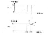
図11は、駆動時間(h)と、有機EL素子からなる発光素子の発光光量との関係を示す特性図である。図11(a)に示すように、各発光素子には一定電圧Vaが印加されているものとする。この場合に、図11(b)に示すように発光光量は、駆動時間が一定時間、この例では200時間まではIaで一定である。駆動時間が200時間を超えると、発光光量はIaからIxのように低下し始め、駆動時間が250時間を超えると、発光光量は更に低下してIyのような特性となる。 FIG. 11 is a characteristic diagram showing the relationship between the driving time (h) and the amount of light emitted from a light emitting element made of an organic EL element. As shown in FIG. 11A, it is assumed that a constant voltage Va is applied to each light emitting element. In this case, as shown in FIG. 11B, the amount of emitted light is constant at Ia until the driving time is constant time, and in this example, up to 200 hours. When the driving time exceeds 200 hours, the amount of emitted light starts to decrease from Ia to Ix, and when the driving time exceeds 250 hours, the amount of emitted light further decreases to become a characteristic like Iy.
前記特許文献1に記載の技術は、発光素子としてLEDの他に有機EL素子を用いることについても言及されている。しかしながら、有機EL素子を定電圧制御する際に、図11のように、駆動時間が一定値を超えると発光光量が低下することの対策については開示されていない。このため、ラインヘッドに有機EL素子を取り付けて駆動する際に、駆動時間が一定値を超えると発光光量が低下して、画質が劣化するという事態に対応できないという問題があった。
The technique described in
本発明は従来技術のこのような問題点に鑑みてなされたものであり、その目的は、有機EL素子を定電流制御することにより、駆動時間が一定時間を超えた場合でも画質が劣化しない構成とした、ラインヘッドおよび画像形成装置を提供することである。 The present invention has been made in view of such problems of the prior art, and an object of the present invention is to control the organic EL element at a constant current so that the image quality does not deteriorate even when the driving time exceeds a certain time. And a line head and an image forming apparatus.
上記目的を達成する本発明のラインヘッドは、1ラインに配列される複数の有機EL素子からなる発光素子と、前記発光素子を定電流制御する手段と、前記発光素子の発光状態の計測手段と、前記計測手段の計測値と基準値との比較手段とを具備し、前記比較手段の出力に基づいて前記発光素子の定電流制御を行うことを特徴とする。このような構成で有機EL素子からなる発光素子を定電流制御することにより、発光素子の経年劣化に伴う発光光量の低下を補償して画質の劣化を防止することができる。 The line head of the present invention that achieves the above object includes a light-emitting element composed of a plurality of organic EL elements arranged in one line, means for controlling the light-emitting element at a constant current, and means for measuring the light emission state of the light-emitting element. And a means for comparing the measured value of the measuring means with a reference value, and performing constant current control of the light emitting element based on the output of the comparing means. By performing constant current control of a light emitting element composed of an organic EL element with such a configuration, it is possible to compensate for a decrease in the amount of light emitted due to aging deterioration of the light emitting element and to prevent deterioration in image quality.
また、本発明のラインヘッドは、前記計測手段は、前記発光素子の駆動電圧を計測することを特徴とする。このように、電気量を計測することにより、駆動時間が一定時間を超えた際に発光光量が低下する、有機EL素子に内在する特有の特性を補償して、画質の劣化を防止することができる。 The line head according to the present invention is characterized in that the measuring means measures a driving voltage of the light emitting element. As described above, by measuring the amount of electricity, it is possible to compensate for the characteristic characteristic inherent in the organic EL element, in which the amount of emitted light decreases when the driving time exceeds a certain time, thereby preventing deterioration of the image quality. it can.
また、本発明のラインヘッドは、前記基準値は前記発光素子で計測される駆動電圧の閾値であることを特徴とする。このように、予め設定されている閾値と発光素子の駆動電圧とを常に対比して定電流制御を行うので、駆動時間が一定時間を超えた際の発光光量の低下を確実に防止することが出来る。 In the line head according to the aspect of the invention, the reference value may be a drive voltage threshold value measured by the light emitting element. As described above, constant current control is performed by always comparing a preset threshold value with the driving voltage of the light emitting element, so that it is possible to reliably prevent a decrease in the amount of emitted light when the driving time exceeds a certain time. I can do it.
また、本発明のラインヘッドは、前記計測手段の計測値によりフィードバック制御で前記発光素子の定電流制御を行うことを特徴とする。このように、常に計測値を定電流制御手段にフィードバックする制御系を構成しているので、発光素子の定電流制御を精度良く行うことができる。 The line head of the present invention is characterized in that constant current control of the light emitting element is performed by feedback control based on a measurement value of the measuring means. Thus, since the control system which always feeds back a measured value to a constant current control means is comprised, the constant current control of a light emitting element can be performed accurately.
また、本発明のラインヘッドは、前記計測手段は、前記発光素子の発光光量を計測することを特徴とする。このように発光素子の光学特性を計測することにより、駆動時間が一定時間を超えた際の発光光量の低下を補償して、画質の劣化を防止することができる。 In the line head according to the invention, the measuring means measures the amount of light emitted from the light emitting element. By measuring the optical characteristics of the light emitting element in this way, it is possible to compensate for a decrease in the amount of emitted light when the driving time exceeds a certain time, and to prevent image quality deterioration.
また、本発明のラインヘッドは、前記発光素子の定電流制御は、個別の発光素子毎に行うことを特徴とする。このように、個別の発光素子毎に定電流制御を行うので、各発光素子の駆動時間が一定値を超えた場合でも高画質の画像形成を行うことができる。 In the line head of the present invention, the constant current control of the light emitting element is performed for each individual light emitting element. As described above, constant current control is performed for each individual light emitting element, so that high-quality image formation can be performed even when the driving time of each light emitting element exceeds a certain value.
また、本発明のラインヘッドは、前記発光素子の定電流制御は、1ラインに配列される複数の発光素子を複数のブロックに区分してブロック単位で行うことを特徴とする。このように、ブロック単位で定電流制御を行うので、種々の画像パターンを形成する際に、画質の劣化を防止することができる。 In the line head of the present invention, the constant current control of the light emitting elements is performed in units of blocks by dividing a plurality of light emitting elements arranged in one line into a plurality of blocks. As described above, constant current control is performed in units of blocks, so that deterioration of image quality can be prevented when various image patterns are formed.
また、本発明のラインヘッドは、前記発光素子の定電流制御は、1ラインに配列される複数の発光素子に対して同時に行うことを特徴とする。
このような構成とすることにより、複数の発光素子に対する定電流制御が簡易化される。
The line head of the present invention is characterized in that the constant current control of the light emitting elements is simultaneously performed on a plurality of light emitting elements arranged in one line.
With such a configuration, constant current control for a plurality of light emitting elements is simplified.
また、本発明のラインヘッドは、前記発光素子の定電流制御は、前記発光素子の駆動時間が一定時間を超えて発光光量が低下した際に、発光光量を所定値に回復させるために駆動電流を段階的に増加させて行うことを特徴とする。このように、発光素子に対する制御は、発光素子の駆動時間に応じて段階的に電流を変えた定電流制御であるので、簡単な手段で画質の劣化を防止することができる。 In the line head according to the present invention, the constant current control of the light emitting element is a driving current for recovering the light emission amount to a predetermined value when the drive amount of the light emitting element exceeds a certain time and the light emission amount decreases. It is characterized in that it is performed in a stepwise manner. As described above, since the control for the light emitting element is constant current control in which the current is changed stepwise according to the driving time of the light emitting element, the image quality can be prevented from being deteriorated by simple means.
また、本発明のラインヘッドは、前記複数の発光素子が配列されるラインを副走査方向に複数列形成したことを特徴とする。このように、ラインヘッドの副走査方向に複数列の発光素子ラインを設けているので、多重露光や予備列の設置などに対応でき、当該ラインヘッドを用いた画像形成装置を多様な用途に適用できる。 The line head according to the present invention is characterized in that a plurality of lines in which the plurality of light emitting elements are arranged are formed in the sub-scanning direction. As described above, since a plurality of light emitting element lines are provided in the sub-scanning direction of the line head, it is possible to cope with multiple exposures, installation of a spare row, and the like, and an image forming apparatus using the line head is applied to various uses. it can.
本発明の画像形成装置は、像担持体の周囲に帯電手段と、前記いずれかに記載のラインヘッドと、現像手段と、転写手段との各画像形成用ユニットを配した画像形成ステーションを少なくとも2つ以上設け、転写媒体が各ステーションを通過することにより、タンデム方式で画像形成を行うことを特徴とする。このため、タンデム方式の画像形成装置において、有機EL素子からなる発光素子の定電流制御を行うことにより、発光素子の駆動時間が一定時間を超えた場合の画質の劣化を防止することができる。 The image forming apparatus according to the present invention includes at least two image forming stations in which image forming units including a charging unit, the line head described above, a developing unit, and a transfer unit are arranged around an image carrier. Two or more are provided, and the image is formed in a tandem manner by passing the transfer medium through each station. For this reason, in the tandem image forming apparatus, by performing constant current control of a light emitting element made of an organic EL element, it is possible to prevent image quality deterioration when the driving time of the light emitting element exceeds a certain time.
また、本発明の画像形成装置は、静電潜像を担持可能に構成された像担持体と、ロータリ現像ユニットと、前記いずれかに記載のラインヘッドとを備え、前記ロータリ現像ユニットは、複数のトナーカートリッジに収納されたトナーをその表面に担持するとともに、所定の回転方向に回転することによって異なる色のトナーを順次前記像担持体との対向位置に搬送し、前記像担持体と前記ロータリ現像ユニットとの間に現像バイアスを印加して、前記トナーを前記ロータリ現像ユニットから前記像担持体に移動させることで、前記静電潜像を顕像化してトナー像を形成することを特徴とする。このため、ロータリ方式の画像形成装置において、有機EL素子からなる発光素子の定電流制御を行うことにより、発光素子の駆動時間が一定時間を超えた場合の画質の劣化を防止することができる。 The image forming apparatus of the present invention includes an image carrier configured to carry an electrostatic latent image, a rotary development unit, and any one of the line heads described above, and the rotary development unit includes a plurality of rotary development units. The toner contained in the toner cartridge is carried on the surface thereof, and the toners of different colors are sequentially conveyed to a position facing the image carrier by rotating in a predetermined rotation direction. A developing bias is applied between the developing unit and the toner is moved from the rotary developing unit to the image carrier, whereby the electrostatic latent image is visualized to form a toner image. To do. For this reason, in a rotary image forming apparatus, by performing constant current control of a light emitting element made of an organic EL element, it is possible to prevent image quality deterioration when the driving time of the light emitting element exceeds a certain time.
また、本発明の画像形成装置は、中間転写部材を備えたことを特徴とする。このため、中間転写部材を備えた画像形成装置において、有機EL素子からなる発光素子の定電流制御を行うことにより、発光素子の駆動時間が一定時間を超えた場合の画質の劣化を防止することができる。 In addition, the image forming apparatus of the present invention includes an intermediate transfer member. For this reason, in an image forming apparatus provided with an intermediate transfer member, by performing constant current control of a light emitting element made of an organic EL element, it is possible to prevent image quality deterioration when the driving time of the light emitting element exceeds a certain time. Can do.
本発明によれば、有機EL素子を定電流制御することにより、駆動時間が一定時間を超えた場合でも画質が劣化しない構成とした、ラインヘッドおよび画像形成装置を得ることができる。 According to the present invention, it is possible to obtain a line head and an image forming apparatus having a configuration in which image quality is not deteriorated even when the driving time exceeds a certain time by performing constant current control of the organic EL element.
以下、図を参照して本発明を説明する。図1は、ラインヘッドに発光素子として有機EL素子を用いた場合の、駆動時間―検出電圧(a)、
駆動時間―駆動電流(b)、駆動時間―発光光量(c)の関係を示す特性図である。図1において、発光素子の駆動開始から200時間経過までの間は、定電流Faで制御する(b)。この間の発光光量は、Iaで一定である(c)。また、発光素子の検出電圧はVaで閾値Vthよりも低くなっている(a)。発光素子の駆動開始から200時間経過した後は、発光光量はIaよりも低下する傾向となっている(c)。これは、有機EL素子の材料などに起因して、温度の上昇に伴う抵抗増加によるもので、同一電流に対して発光効率が低下するためである。
The present invention will be described below with reference to the drawings. FIG. 1 shows a driving time-detection voltage (a) when an organic EL element is used as a light emitting element in a line head.
It is a characteristic view showing the relationship of drive time-drive current (b), drive time-light emission quantity (c). In FIG. 1, the constant current Fa is used for control from the start of driving the light emitting element to 200 hours (b). The amount of light emitted during this period is constant at Ia (c). Further, the detection voltage of the light emitting element is Va, which is lower than the threshold value Vth (a). After 200 hours from the start of driving the light emitting element, the amount of emitted light tends to be lower than Ia (c). This is because, due to the material of the organic EL element, etc., it is due to an increase in resistance as the temperature rises, and the light emission efficiency is reduced for the same current.
このように、発光素子の駆動開始から200時間経過した後には、発光素子の抵抗が増加しているので、発光素子に定電流を流している場合には、検出電圧は上昇する(a)。本発明においては、発光素子を定電流制御する際に、発光素子の電圧を検出して予め設定されている閾値電圧Vth(基準値)と比較して、検出電圧が閾値電圧Vthを超えた場合には、駆動電流をFbに引き上げて定電流制御を行う(b)。 As described above, after 200 hours have elapsed from the start of driving of the light emitting element, the resistance of the light emitting element increases, and therefore, when a constant current is passed through the light emitting element, the detection voltage increases (a). In the present invention, when the current of the light emitting element is controlled at a constant current, the voltage of the light emitting element is detected and compared with a preset threshold voltage Vth (reference value), when the detected voltage exceeds the threshold voltage Vth The constant current control is performed by raising the drive current to Fb (b).
このように、駆動電流をFaからFbに引き上げて定電流制御を行うタイミングは、図1の例では発光素子の駆動時間が250時間を超えた時点である。この際に、発光光量はIxからIbに回復し、駆動当初の発光光量Iaとほぼ等しくなる(c)。また、発光素子の検出電圧は、VxからVbに上昇する。 As described above, the timing for performing the constant current control by raising the drive current from Fa to Fb is the time when the drive time of the light emitting element exceeds 250 hours in the example of FIG. At this time, the amount of emitted light recovers from Ix to Ib, and becomes substantially equal to the amount of emitted light Ia at the beginning of driving (c). Further, the detection voltage of the light emitting element rises from Vx to Vb.
図1(c)から明らかなように、発光素子を定電流制御している際に、発光素子の駆動時間が一定時間、例えば200時間を超えて250時間に接近すると、発光光量が低下して所望の画像形成ができなくなる。この際に、発光素子の検出電圧は図1(a)に示されているように、基準値(閾値電圧Vth)のレベルに近づく。 As can be seen from FIG. 1C, when the light emitting element is under constant current control and the driving time of the light emitting element approaches a certain time, for example, more than 200 hours and approaches 250 hours, the amount of emitted light decreases. A desired image cannot be formed. At this time, the detection voltage of the light emitting element approaches the level of the reference value (threshold voltage Vth) as shown in FIG.
したがって、定電流制御を行う際に、図1(c)に示されているように、発光素子の発光光量をセンサで検出することにより、発光光量の経時変化を判断して画質劣化を未然に防止するように段階的に電流を増加させる制御を行うことができる。また、図1(a)に示されているように、発光素子の駆動電圧を検出することにより、同様に発光光量の経時変化を判断して、画質劣化を未然に防止するように段階的に電流を増加させる制御を行うことができる。 Accordingly, when constant current control is performed, as shown in FIG. 1C, the amount of light emitted from the light emitting element is detected by the sensor, so that a change in the amount of light emitted with time is judged and image quality deterioration is prevented. Control to increase the current step by step can be performed so as to prevent it. In addition, as shown in FIG. 1A, by detecting the driving voltage of the light emitting element, the change in the amount of emitted light is similarly judged in a stepwise manner so as to prevent image quality deterioration in advance. Control for increasing the current can be performed.
図1(a)〜(c)の例は、発光素子の駆動時間に応じて駆動電流を変えて発光素子を定電流制御するものである。このように、本発明の実施形態にかかる発光素子に対する電流制御は、発光素子の駆動時間に応じて段階的に印加する電流値を変えた定電流制御であるので、簡単な手段で画質の劣化を防止することができる。 In the example of FIGS. 1A to 1C, the driving current is changed according to the driving time of the light emitting element to control the light emitting element at a constant current. As described above, the current control for the light emitting element according to the embodiment of the present invention is a constant current control in which the current value to be applied is changed stepwise according to the driving time of the light emitting element. Can be prevented.
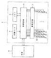
図2は、画像形成装置の概略構成を示すブロック図である。図2において、2はラインヘッドの制御部、3は制御回路、4はTFTからなる駆動回路、5は電圧検出器、6はメモリ、7は発光素子Eaが1ライン(主走査方向)に複数配列され、副走査方向に複数列設けられている発光素子ライン、8は本体コントローラである。電圧検出器5で検出された各発光素子の駆動電圧は、制御回路3にフィードバックされる。
FIG. 2 is a block diagram illustrating a schematic configuration of the image forming apparatus. In FIG. 2, 2 is a control unit of the line head, 3 is a control circuit, 4 is a drive circuit comprising TFTs, 5 is a voltage detector, 6 is a memory, and 7 is a plurality of light emitting elements Ea in one line (main scanning direction). A light emitting
本体コントローラ8は、印刷データを形成してラインヘッドの制御部2に送信する。メモリ6には、各発光素子Eaの特性、例えば図1(a)に示したような閾値電圧Vth、図1(c)に示したような駆動時間―発光光量の特性を記憶させている。本体コントローラ8は、図1(b)に示したような駆動時間―印加電流の特性を作成して制御回路3に送信する。制御回路3は、当該特性をメモリ6に記憶させる。
The
制御回路3は、前記閾値電圧Vthをメモリ6から読み出し、フィードバックされた発光素子の検出電圧と対比する。対比した結果に基づいて各発光素子の制御信号を形成し、駆動回路4を動作させて各発光素子の定電流制御を行う。このように、駆動回路4により個別の発光素子毎に定電流制御を行うので、各発光素子の駆動時間が一定値を超えた場合でも高画質の画像形成を行うことができる。
The
なお、駆動回路4は、個別の発光素子Eaに対してそれぞれ所定電流を印加して定電流制御を行うが、主走査方向の1ラインすべての発光素子に対して、同じ電流で駆動することも可能である。個々の発光素子の発光特性は異なるが、同一電流で駆動しても画質劣化の度合いは有意の形態とはならない。このような構成とすることにより、複数の発光素子に対する定電流制御が簡易化される。 The driving circuit 4 performs constant current control by applying a predetermined current to each individual light emitting element Ea. However, all the light emitting elements in one line in the main scanning direction may be driven with the same current. Is possible. Although the light emitting characteristics of the individual light emitting elements are different, the degree of image quality deterioration does not become a significant form even when driven by the same current. With such a configuration, constant current control for a plurality of light emitting elements is simplified.
図2の例では、ラインヘッドの副走査方向に複数列の発光素子ラインを設けている。このため、ラインヘッドを多重露光に適用することができる。また、主走査方向の1ラインで画像形成を行い、他のラインは前記画像形成ラインの故障時の予備用に用いることもできる。このように、図2の例では、ラインヘッドの副走査方向に複数列の発光素子ラインを設けているので、画像形成装置を多様な用途に適用できる。 In the example of FIG. 2, a plurality of light emitting element lines are provided in the sub-scanning direction of the line head. For this reason, the line head can be applied to multiple exposure. Further, image formation can be performed with one line in the main scanning direction, and the other lines can be used for backup when the image forming line fails. As described above, in the example of FIG. 2, since the light emitting element lines of a plurality of columns are provided in the sub-scanning direction of the line head, the image forming apparatus can be applied to various uses.
図3は、本発明の他の実施形態を示すブロック図である。図3においては、図2で示した電圧検出器5に代えて、光量センサ9を設け、光量センサ9の計測信号を制御回路3に入力している。本体コントローラ8は、図1(c)に示した発光素子の駆動時間―発光光量の特性を制御回路3に送信する。制御回路3は、当該特性をメモリ6に記憶させる。
FIG. 3 is a block diagram showing another embodiment of the present invention. In FIG. 3, instead of the
発光素子を駆動する際に、制御回路3は前記特性をメモリ6から読み出し、光量センサ9の計測信号と対比する。光量センサ9の計測値は、発光素子の駆動時間が200時間を超えると、図1(c)の特性Ixに沿って低下する。さらに発光素子の駆動時間が累積されて、駆動時間が250時間に到達すると、発光光量の値はIyまで低下する。この際に、制御回路3は、駆動電流をIaからIbに上昇させて、図2と同様に各発光素子の定電流制御を行う。すなわち、駆動時間が250時間に到達したときの発光光量Iyは、駆動電流をFaからFbに引き上げるかどうかを判断する際の基準値となる。
When driving the light emitting element, the
本発明のラインヘッドは、図2、図3のように副走査方向に複数列の発光素子ラインを設けた例には限定されない。図4は、本発明の他の実施形態にかかるラインヘッドの説明図である。図4の例では、ラインヘッド10には、1ラインの発光素子ライン1が設けられている。この発光素子ライン1には、有機EL素子からなる複数の発光素子Eaが配列されている。
The line head of the present invention is not limited to an example in which a plurality of light emitting element lines are provided in the sub-scanning direction as shown in FIGS. FIG. 4 is an explanatory diagram of a line head according to another embodiment of the present invention. In the example of FIG. 4, the
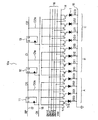
また、発光素子ライン1は、A、B、C・・・Nの複数のブロックに区分されている。本発明の実施形態においては、前記図1(a)に示したような定電流制御を、図2、図3で説明したように各発光素子単位、すなわち、各ドット単位で行う外に、図4に示したようなブロック単位で行うこともできる。このように、ブロック単位で電圧制御を行う場合には、種々の画像パターンを形成する際に、画質の劣化を防止することができる。次に、ブロック単位で電圧制御する具体例について、図5の回路図で説明する。
The light emitting
図5において、ラインヘッド10aには、発光素子ライン1が設けられている。発光素子ライン1には、有機EL素子を用いた発光素子D00〜D23が配列されている。14は正の電源線、15は負の電源線である。正の電源線14は、発光素子ライン1における各発光素子のアノードに共通して接続されている。また、負の電源線15は発光素子ライン1における各発光素子のカソードに接続されている。発光素子ライン1は、電源線14、15間に接続される。
In FIG. 5, the light emitting
図5の11、12、13は、発光素子D00〜D23をブロック単位で制御するためのシフトレジスタ回路で、シフトレジスタ回路11の出力信号C0は発光素子D00〜D03を含むブロックAを制御する。また、シフトレジスタ回路12の出力信号C1は発光素子D10〜D13を含むブロックBを制御し、シフトレジスタ回路13の出力信号C2は発光素子D20〜D23を含むブロックCを制御する。
SPは信号線17よりシフトレジスタ11のデータ端子Dに入力されるスタートパルス、CKは信号線18より各シフトレジスタ11〜13に入力されるクロック信号である。16は各発光素子にデータ信号Dat0〜Dat3を供給する信号線、Tr2は各発光素子のアノード側に接続されるドライバトランジスタ、Tr1はドライバトランジスタTr2のゲートにソースが接続される制御トランジスタである。制御トランジスタTr1、ドライバトランジスタTr2は、例えばFET(Field Effect Transistor、電界効果トランジスタ)により形成される。
SP is a start pulse input to the data terminal D of the
シフトレジスタ回路11の出力端子Qから出力される出力信号C0は、信号線C0aを介して発光素子D00〜D03に接続される各制御トランジスタTr1のゲートに印加される。C1はシフトレジスタ回路12の出力信号であり、信号線C1aを介して発光素子D10〜D13に接続される各制御トランジスタTr1のゲートに印加される。C2はシフトレジスタ回路13の出力信号であり、信号線C2aを介して発光素子D20〜D23に接続される各制御トランジスタTr1のゲートに印加される。
The output signal C0 output from the output terminal Q of the
このように、シフトレジスタ回路11は発光素子ライン1の発光素子の中からブロックAの発光素子D00〜D03を選択する。また、シフトレジスタ回路12はブロックBの発光素子D10〜D13を選択し、シフトレジスタ回路13はブロックCの発光素子D20〜D23を選択する。すなわち、シフトレジスタ回路11〜13は、発光素子のブロック選択手段として機能する。
Thus, the
それぞれのシフトレジスタ回路の出力信号C0〜C2がHレベルのときに、当該ブロックの発光素子を制御する各制御トランジスタTr1のゲートに信号を印加する。各発光素子は、正の電圧VDDが印加される電源線14と負の電源線15間に並列に接続されている。このようにシフトレジスタを用いているので、パルス駆動の簡単な構成でブロック選択を行うことができる。
When the output signals C0 to C2 of the respective shift register circuits are at the H level, a signal is applied to the gate of each control transistor Tr1 that controls the light emitting elements of the block. Each light emitting element is connected in parallel between a
次に、データ線16のデータ信号Dat0〜Dat3について説明する。このデータ信号は、各制御トランジスタTr1のドレインに供給される。したがって、前記ブロック選択信号で選択された発光素子の制御トランジスタTr1にデータ信号Dat0〜Dat3が供給されると、当該制御トランジスタTr1に接続されたドライバトランジスタTr2が導通して該当する発光素子が動作する。なお、前記ブロック選択信号を制御トランジスタTr1のドレインに、データ線を制御トランジスタTr1のゲートに繋ぎ変えた構成でも同様の動作が可能である。
Next, the data signals Dat0 to Dat3 of the
例えばブロックAについては、データ信号Dat0〜Dat3はそれぞれ発光素子D00〜D03を制御する制御トランジスタTr1に供給される。すなわち、データ信号Dat0〜Dat3は、同一ブロック内の個別の発光素子を選択する選択信号として作用する。このように、本発明のラインヘッドにおいては、個別の発光素子を選択して点灯動作させることができる。なお、データ信号Dat0〜Dat3は、濃淡データが時間データに変換されて各発光素子に供給される。 For example, for the block A, the data signals Dat0 to Dat3 are supplied to the control transistor Tr1 that controls the light emitting elements D00 to D03, respectively. That is, the data signals Dat0 to Dat3 act as selection signals for selecting individual light emitting elements in the same block. As described above, in the line head of the present invention, individual light emitting elements can be selected and lit. The data signals Dat0 to Dat3 are supplied to each light emitting element after the grayscale data is converted into time data.
図5においては、前記のようにシフトレジスタ回路11〜13が、発光素子のブロック選択手段として機能している。シフトレジスタ回路11〜13で選択されたブロックA、B、Cの各発光素子に、電源線14から正の電圧VDDを供給することにより、初期のVaによる定電圧制御を行う。また、図1(a)に示したようなVaからVbに昇圧した電圧による定電圧制御を行うことができる。
In FIG. 5, as described above, the
図6は、発光素子の定電流制御の例を示す回路図、図7はドライバトランジスタTr2、および有機EL素子からなる発光素子Eaの動作原理を示す特性図である。図6に示された駆動方式は、電流プログラム階調と呼ばれている。 FIG. 6 is a circuit diagram showing an example of constant current control of a light emitting element, and FIG. 7 is a characteristic diagram showing an operation principle of a light emitting element Ea composed of a driver transistor Tr2 and an organic EL element. The driving method shown in FIG. 6 is called current program gradation.
この電流プログラム階調は、発光ポリマーディスプレイ用に開発されたものである(工業調査会「電子材料」7月号別冊「液晶ディスプレイ技術2001年」(2001年7月発行)「低温poly-Si 薄膜トランジスタ駆動発光ポリマーディスプレイ」)。電流プログラム階調は、全ての特性バラツキに起因する発光輝度バラツキを抑制するためのものである。 This current program gradation has been developed for light-emitting polymer displays (Industrial Research Committee "Electronic Materials" July issue separate volume "Liquid Crystal Display Technology 2001" (issued July 2001) "Low-temperature poly-Si thin film transistor Driven light emitting polymer display "). The current program gradation is for suppressing variations in light emission luminance due to all characteristic variations.
図6において、MN1は、有機EL素子からなる発光素子(OLED)の選択信号が入力されるトランジスタ、MN2はドライバトランジスタ、MN3は定電流源(IData)の電流を供給するトランジスタ、MN4は電源電圧(VDD)をオン、オフするスイッチングトランジスタである。C1は、ドライバトランジスタMN2のゲート電極とドレイン電極間に接続されるコンデンサである。各トランジスタMN1〜MN4は、TFTで構成される。 In FIG. 6, MN1 is a transistor to which a selection signal of a light emitting element (OLED) made of an organic EL element is input, MN2 is a driver transistor, MN3 is a transistor for supplying a constant current source (IDdata) current, and MN4 is a power supply voltage. This is a switching transistor that turns on and off (VDD). C1 is a capacitor connected between the gate electrode and the drain electrode of the driver transistor MN2. Each of the transistors MN1 to MN4 is composed of a TFT.
図7には、ドライバトランジスタMN2のドレインーソース電流(Ids)と、ドレインーソース電圧(Vds)の関係の特性が示されている。また、発光素子(OLED)電流―電圧特性が示されている。プログラム電流は、定電流制御の目標値に相当する。 FIG. 7 shows characteristics of the relationship between the drain-source current (Ids) of the driver transistor MN2 and the drain-source voltage (Vds). In addition, light-emitting element (OLED) current-voltage characteristics are shown. The program current corresponds to a target value for constant current control.
電流プログラム期間(定電流制御期間)には、TFTのゲート電極とドレイン電極を短絡させてVgs=Vdsとし、階調信号はアナログ電流としてTFTに供給され、このときのVgsをコンデンサC1に記憶させる。保持期間には、アナログ電流は定電圧VDDに切り換えられて、動作点はTFTと発光素子OLEDのI−V特性の交点となる。TFTは電流プログラム期間・保持期間とも飽和領域で動作しているので、プログラム電流と同量の電流が保持期間にも供給される。すなわち、発光素子は定電流制御される。 In the current program period (constant current control period), the gate electrode and drain electrode of the TFT are short-circuited to Vgs = Vds, and the gradation signal is supplied to the TFT as an analog current, and Vgs at this time is stored in the capacitor C1. . In the holding period, the analog current is switched to the constant voltage VDD, and the operating point is an intersection of the IV characteristics of the TFT and the light emitting element OLED. Since the TFT operates in the saturation region in both the current program period and the holding period, the same amount of current as the program current is supplied to the holding period. That is, the light emitting element is controlled with constant current.
この電流プログラム階調の特徴は、TFTの飽和領域を利用しているので、TFT・発光素子の全ての特性バラツキに起因する発光輝度バラツキの抑制が可能なことである。また、定電流制御でありながら、発光部の数だけ定電流源を必要とせず、1つの定電圧源VDDに接続すればよいので、構成が簡単になる。 A feature of this current program gradation is that since the saturation region of the TFT is used, it is possible to suppress variations in light emission luminance caused by variations in characteristics of all TFTs and light emitting elements. In addition, although the constant current control is used, the number of light emitting units is not required and constant current sources are not required, and it is only necessary to connect to one constant voltage source VDD.
図8は、本発明の画像形成装置の制御部の構成を示すブロック図である。図8の画像形成装置では、ユーザからの画像形成要求に応じて、ホストコンピュータなどの外部装置から画像信号がメインコントローラ11に与えられる。この際に、メインコントローラ20からエンジンコントローラ30に指令信号が送信される。この指令信号に応じてエンジンコントローラ30がエンジン部EGの各部を制御して、記録媒体に画像信号に対応する画像を形成する。
FIG. 8 is a block diagram showing the configuration of the control unit of the image forming apparatus of the present invention. In the image forming apparatus of FIG. 8, an image signal is given to the
このエンジン部EGにおいては、帯電ユニット62は帯電制御部103から帯電バイアスが印加されており、感光体の外周面を所定の表面電位に均一に帯電させる。そして、この帯電ユニット62によって帯電された感光体の外周面に向けて露光ユニット61から光ビームが照射される。この露光ユニット61は、露光制御部102から与えられる制御指令に応じて光ビームを感光体上に露光して、画像信号に対応する静電潜像を形成する。露光ユニット61には、レンズ、ミラーなどの適宜の光学素子が設けられている。
In the engine unit EG, the charging
ホストコンピュータなどの外部装置より、インターフェース112を介してメインコントローラ20のCPU111に画像信号が与えられると、エンジンコントローラ30のCPU101が露光制御部102に対し所定のタイミングで画像信号に対応した制御信号を出力する。この制御信号に応じて露光ユニット61から光ビームが感光体上に照射されて、画像信号に対応する静電潜像が感光体上に形成される。
When an image signal is given from an external device such as a host computer to the
現像ユニット40は、現像器制御部104により制御されている。ここで、現像器制御部104から直流電圧と交流電圧とが重畳された現像バイアスが現像ローラに印加される。このような現像バイアスによって、現像ローラ上に担持されたトナーは、感光体の表面各部にその表面電位に応じて部分的に付着し、こうして感光体上の静電潜像が当該トナー色のトナー像として顕像化される。
The developing
垂直同期センサ64は、中間転写ベルトの基準位置を検出するためのセンサであり、中間転写ベルトの回転駆動に関連して出力される同期信号、つまり垂直同期信号Vsyncを得るための垂直同期センサとして機能する。そして、この装置では、各部の動作タイミングを揃えるとともに各色で形成されるトナー像を正確に重ね合わせるために、装置各部の動作はこの垂直同期信号Vsyncに基づいて制御される。
The
さらに、濃度センサ63は、中間転写ベルトの表面に対向して設けられており、濃度制御処理において、中間転写ベルトの外周面に形成されるパッチ画像の光学濃度を測定する。光量センサ65は、図3の光量センサ9に対応する。また、図示を省略しているが、図2で説明した電圧検出器を設けて発光素子の検出電圧をCPU101に入力する構成とすることもできる。
Further, the
図8に示すように、各現像器(トナーカートリッジ)48Y、48C、48M、48Kには、該現像器の製造ロットや使用履歴、内蔵トナーの残量などに関するデータを記憶する「記憶素子」であるメモリ91〜94がそれぞれ設けられている。さらに、各現像器48Y、48C、48M、48Kには、コネクタ49Y、49C、49M、49Kがそれぞれ設けられている。
As shown in FIG. 8, each developing device (toner cartridge) 48Y, 48C, 48M, 48K is a “storage element” that stores data relating to the manufacturing lot and usage history of the developing device, the remaining amount of built-in toner, and the like. Certain memories 91 to 94 are provided. Further,
そして、必要に応じて、これらのコネクタ49Y、49C、49M、49Kが選択的に本体側に設けられたコネクタ108と接続される。このため、インターフェース105を介して、エンジンコントローラ30のCPU101と各メモリ91〜94との間でデータの送受を行って、該現像器(トナーカートリッジ)に関する消耗品管理等の各種情報の管理を行っている。なお、この実施形態では、本体側コネクタ108と各現像器側のコネクタ49K等とが機械的に嵌合することで相互にデータ送受を行っているが、例えば無線通信等の電磁的手段を用いて非接触にてデータ送受を行うようにしてもよい。
If necessary, these
また、各現像器48Y、48C、48M、48Kに固有のデータを記憶するメモリ91〜94は、電源オフ状態や該現像器が本体から取り外された状態でもそのデータを保存できる不揮発性メモリであることが望ましい。このような不揮発性メモリとしては、例えばフラッシュメモリや強誘電体メモリ(FRAM:Ferroelectric Ramdom Access Memory)、EEPROMなどを用いることができる。
The memories 91 to 94 for storing data unique to each of the developing
また、この画像形成装置では図8に示すように表示部21が設けられている。そして、必要に応じCPU111から与えられる制御指令に応じて所定のメッセージを表示することで、必要な情報をユーザに対し報知する。例えば、装置の故障や紙詰まり等の異常が発生したときにはその旨をユーザに知らせるメッセージを表示する。また、いずれかの現像器内のトナー残量が所定値以下、例えば後述するニアエンド値まで低下したときには、当該現像器の交換を促すメッセージを表示する。
Further, in this image forming apparatus, a
この表示部21としては、例えば液晶ディスプレイ等の表示装置を用いることができるが、これ以外に、必要に応じて点灯あるいは点滅する警告ランプを用いてもよい。さらに、メッセージを表示することで視覚によりユーザに報知する以外に、予め録音された音声メッセージやブザー等の音声による警報装置を用いたり、これらを適宜組み合わせて使用してもよい。
As the
ホストコンピュータなどの外部装置よりインターフェース112を介して与えられた画像を記憶するために、画像メモリ113が設けられている。符号106はCPU101が実行する演算プログラムやエンジン部EGを制御するための制御データなどを記憶するためのROM、また符号107はCPU101における演算結果やその他のデータを一時的に記憶するRAMである。RAM107は、FRAMを用いても良い。
An
本発明においては、上記のような構成の有機ELアレイヘッドを、例えば電子写真方式のカラー画像を形成する画像形成装置の露光ヘッドとして用いることができる。図9は、有機ELアレイヘッドを用いた画像形成装置の一例を示す正面図である。この画像形成装置は、同様な構成の4個の有機ELアレイ露光ヘッド101K、101C、101M、101Yを、対応する同様な構成である4個の感光体ドラム(像担持体)41K、41C、41M、41Yの露光位置にそれぞれ配置したものであり、タンデム方式の画像形成装置として構成されている。 In the present invention, the organic EL array head configured as described above can be used as, for example, an exposure head of an image forming apparatus that forms an electrophotographic color image. FIG. 9 is a front view showing an example of an image forming apparatus using an organic EL array head. This image forming apparatus includes four organic EL array exposure heads 101K, 101C, 101M, and 101Y having the same configuration and corresponding four photosensitive drums (image carriers) 41K, 41C, and 41M having the same configuration. , 41Y, respectively, and is configured as a tandem image forming apparatus.
図9に示すように、この画像形成装置は、駆動ローラ51と従動ローラ52とテンションローラ53が設けられており、テンションローラ53によりテンションを加えて張架されて、図示矢印方向(反時計方向)へ循環駆動される中間転写ベルト50を備えている。この中間転写ベルト50に対して所定間隔で配置された4個の像担持体としての外周面に感光層を有する感光体41K、41C、41M、41Yが配置される。
As shown in FIG. 9, this image forming apparatus is provided with a
前記符号の後に付加されたK、C、M、Yはそれぞれ黒、シアン、マゼンタ、イエローを意味し、それぞれ黒、シアン、マゼンタ、イエロー用の感光体であることを示す。他の部材についても同様である。感光体41K、41C、41M、41Yは、中間転写ベルト50の駆動と同期して図示矢印方向(時計方向)へ回転駆動される。
K, C, M, and Y added after the reference sign mean black, cyan, magenta, and yellow, respectively, and indicate that the photoconductors are black, cyan, magenta, and yellow, respectively. The same applies to other members. The
各感光体41(K、C、M、Y)の周囲には、それぞれ感光体41(K、C、M、Y)の外周面を一様に帯電させる帯電手段(コロナ帯電器)42(K、C、M、Y)と、この帯電手段42(K、C、M、Y)により一様に帯電させられた外周面を感光体41(K、C、M、Y)の回転に同期して順次ライン走査する本発明の上記のような有機ELアレイ露光ヘッド1(K、C、M、Y)が設けられている。 Around each photoconductor 41 (K, C, M, Y), charging means (corona charger) 42 (K) for uniformly charging the outer peripheral surface of the photoconductor 41 (K, C, M, Y), respectively. , C, M, Y) and the outer peripheral surface uniformly charged by the charging means 42 (K, C, M, Y) are synchronized with the rotation of the photoconductor 41 (K, C, M, Y). Thus, the organic EL array exposure head 1 (K, C, M, Y) as described above of the present invention for sequentially scanning the lines is provided.
また、この有機ELアレイ露光ヘッド101(K、C、M、Y)で形成された静電潜像に現像剤であるトナーを付与して可視像(トナー像)とする現像装置44(K、C、M、Y)と、この現像装置44(K、C、M、Y)で現像されたトナー像を一次転写対象である中間転写ベルト50に順次転写する転写手段としての一次転写ローラ45(K、C、M、Y)と、転写された後に感光体41(K、C、M、Y)の表面に残留しているトナーを除去するクリーニング手段としてのクリーニング装置46(K、C、M、Y)とを有している。
Further, a developing device 44 (K) that applies toner as a developer to the electrostatic latent image formed by the organic EL array exposure head 101 (K, C, M, Y) to form a visible image (toner image). , C, M, Y) and a primary transfer roller 45 as transfer means for sequentially transferring the toner image developed by the developing device 44 (K, C, M, Y) to the
ここで、各有機ELアレイ露光ヘッド101(K、C、M、Y)は、有機ELアレイ露光ヘッド101(K、C、M、Y)のアレイ方向が感光体ドラム41(K、C、M、Y)の母線に沿うように設置される。そして、各有機ELアレイ露光ヘッド101(K、C、M、Y)の発光エナルギーピーク波長と感光体41(K、C、M、Y)の感度ピーク波長とは略一致するように設定されている。 Here, in each organic EL array exposure head 101 (K, C, M, Y), the array direction of the organic EL array exposure head 101 (K, C, M, Y) is the photosensitive drum 41 (K, C, M). , Y) along the bus. The light emission energy peak wavelength of each organic EL array exposure head 101 (K, C, M, Y) and the sensitivity peak wavelength of the photoconductor 41 (K, C, M, Y) are set to substantially coincide with each other. Yes.
現像装置44(K、C、M、Y)は、例えば、現像剤として非磁性一成分トナーを用いるもので、その一成分現像剤を例えば供給ローラで現像ローラへ搬送し、現像ローラ表面に付着した現像剤の膜厚を規制ブレードで規制し、その現像ローラを感光体41(K、C、M、Y)に接触あるいは押厚させることにより、感光体41(K、C、M、Y)の電位レベルに応じて現像剤を付着させることによりトナー像として現像するものである。 The developing device 44 (K, C, M, Y) uses, for example, a non-magnetic one-component toner as a developer, and the one-component developer is conveyed to the developing roller by a supply roller, for example, and adheres to the surface of the developing roller. The film thickness of the developed developer is regulated by a regulating blade, and the developing roller is brought into contact with or increased in thickness by the photosensitive body 41 (K, C, M, Y), whereby the photosensitive body 41 (K, C, M, Y). The toner is developed as a toner image by attaching a developer according to the potential level.
このような4色の単色トナー像形成ステーションにより形成された黒、シアン、マゼンタ、イエローの各トナー像は、一次転写ローラ45(K、C、M、Y)に印加される一次転写バイアスにより中間転写ベルト50上に順次一次転写され、中間転写ベルト50上で順次重ね合わされてフルカラーとなったトナー像は、二次転写ローラ66において用紙等の記録媒体Pに二次転写され、定着部である定着ローラ対61を通ることで記録媒体P上に定着され、排紙ローラ対62によって、装置上部に形成された排紙トレイ68上へ排出される。
The black, cyan, magenta, and yellow toner images formed by the four-color single-color toner image forming station are intermediated by the primary transfer bias applied to the primary transfer roller 45 (K, C, M, Y). The toner image, which is sequentially primary transferred onto the
なお、図9中、63は多数枚の記録媒体Pが積層保持されている給紙カセット、64は給紙カセット63から記録媒体Pを一枚ずつ給送するピックアップローラ、65は二次転写ローラ66の二次転写部への記録媒体Pの供給タイミングを規定するゲートローラ対、66は中間転写ベルト50との間で二次転写部を形成する二次転写手段としての二次転写ローラ、67は二次転写後に中間転写ベルト50の表面に残留しているトナーを除去するクリーニング手段としてのクリーニングブレードである。記録媒体Pの搬送経路の適宜の位置、例えば給紙カセット63とゲートローラ対65間の適宜の位置には、印字される記録紙の枚数をカウントするカウンタを設ける。
In FIG. 9,
このように、図9の画像形成装置は、書き込み手段として有機ELアレイを用いているので、レーザ走査光学系を用いた場合よりも、装置の小型化を図ることができる。本発明においては、図9に示したようなタンデム方式の画像形成装置において、発光素子の定電流制御を行う際に、発光素子の駆動時間が一定時間を超えた場合の画質の劣化を防止することができる。 As described above, since the image forming apparatus of FIG. 9 uses the organic EL array as the writing means, the apparatus can be made smaller than when the laser scanning optical system is used. In the present invention, in the tandem image forming apparatus as shown in FIG. 9, when performing constant current control of the light emitting element, deterioration of image quality when the driving time of the light emitting element exceeds a certain time is prevented. be able to.
次に、本発明に係る画像形成装置に係る他の実施の形態について説明する。図10は、画像形成装置の縦断側面図である。図10において、画像形成装置160には主要構成部材として、ロータリ構成の現像装置161、像担持体として機能する感光体ドラム165、有機ELアレイが設けられている像書込手段(ラインヘッド)167、中間転写ベルト169、用紙搬送路174、定着器の加熱ローラ172、給紙トレイ178が設けられている。
Next, another embodiment of the image forming apparatus according to the present invention will be described. FIG. 10 is a vertical side view of the image forming apparatus. In FIG. 10, the
現像装置161は、現像ロータリ161aが軸161bを中心として矢視A方向に回転する。現像ロータリ161aの内部は4分割されており、それぞれイエロー(Y)、シアン(C)、マゼンタ(M)、ブラック(K)の4色の像形成ユニットが設けられている。162a〜162dは、前記4色の各像形成ユニットに配置されており、矢視B方向に回転する現像ローラ、163a〜163dは、矢視C方向に回転するトナ−供給ローラである。また、164a〜164dはトナーを所定の厚さに規制する規制ブレードである。
In the developing
165は、前記のように像担持体として機能する感光体ドラム、166は一次転写部材、168は帯電器、167は像書込手段で有機ELアレイが設けられている。感光体ドラム165は、図示を省略した駆動モータ、例えばステップモータにより現像ローラ162aとは逆方向の矢視D方向に駆動される。
As described above,
中間転写ベルト169は、従動ローラ170bと駆動ローラ170a間に張架されており、駆動ローラ170aが前記感光体ドラム165の駆動モータに連結されて、中間転写ベルトに動力を伝達している。当該駆動モータの駆動により、中間転写ベルト169の駆動ローラ170aは感光体ドラム165とは逆方向の矢視E方向に回動される。
The
用紙搬送路174には、複数の搬送ローラと排紙ローラ対176などが設けられており、用紙を搬送する。中間転写ベルト169に担持されている片面の画像(トナー像)が、二次転写ローラ171の位置で用紙の片面に転写される。二次転写ローラ171は、クラッチにより中間転写ベルト169に離当接され、クラッチオンで中間転写ベルト169に当接されて用紙に画像が転写される。
The
上記のようにして画像が転写された用紙は、次に、定着ヒータを有する定着器で定着処理がなされる。定着器には、加熱ローラ172、加圧ローラ173が設けられている。定着処理後の用紙は、排紙ローラ対176に引き込まれて矢視F方向に進行する。この状態から排紙ローラ対176が逆方向に回転すると、用紙は方向を反転して両面プリント用搬送路175を矢視G方向に進行する。177は電装品ボックス、178は用紙を収納する給紙トレイ、179は給紙トレイ178の出口に設けられているピックアップローラである。印字される記録紙の枚数は、給紙トレイ近傍など、給紙搬送路の適宜の位置に設けられるセンサによりカウントされる。
The sheet on which the image has been transferred as described above is then subjected to a fixing process by a fixing device having a fixing heater. The fixing device is provided with a heating roller 172 and a pressure roller 173. The sheet after the fixing process is drawn into the
用紙搬送路において、搬送ローラを駆動する駆動モータは、例えば低速のブラシレスモータが用いられる。また、中間転写ベルト169は色ずれ補正などが必要となるのでステップモータが用いられている。これらの各モータは、図示を省略している制御手段からの信号により制御される。
For example, a low-speed brushless motor is used as a drive motor for driving the transport roller in the paper transport path. The
図の状態で、イエロー(Y)の静電潜像が感光体ドラム165に形成され、現像ローラ62aに高電圧が印加されることにより、感光体ドラム165にはイエローの画像が形成される。イエローの裏側および表側の画像がすべて中間転写ベルト169に担持されると、現像ロータリ161aが矢視A方向に90度回転する。
In the state shown in the drawing, a yellow (Y) electrostatic latent image is formed on the
中間転写ベルト169は1回転して感光体ドラム165の位置に戻る。次にシアン(C)の2面の画像が感光体ドラム165に形成され、この画像が中間転写ベルト169に担持されているイエローの画像に重ねて担持される。以下、同様にして現像ロータリ161の90度回転、中間転写ベルト169への画像担持後の1回転処理が繰り返される。
The
4色のカラー画像担持には中間転写ベルト169は4回転して、その後に更に回転位置が制御されて二次転写ローラ171の位置で用紙に画像を転写する。給紙トレー178から給紙された用紙を搬送路174で搬送し、二次転写ローラ171の位置で用紙の片面に前記カラー画像を転写する。片面に画像が転写された用紙は前記のように排紙ローラ対176で反転されて、搬送径路で待機している。その後、用紙は適宜のタイミングで二次転写ローラ171の位置に搬送されて、他面に前記カラー画像が転写される。ハウジング180には、排気ファン181が設けられている。
For carrying four color images, the
本発明においては、図10に示したようなロータリ方式の画像形成装置において、発光素子の定電流制御を行う際に、発光素子の駆動時間が一定時間を超えた場合の画質の劣化を防止することができる。また、中間転写部材を備えたタンデム方式およびロータリ方式の画像形成装置において、発光素子の定電流制御を行う際に、発光素子の駆動時間が一定時間を超えた場合の画質の劣化を防止することができる。 In the present invention, in the rotary type image forming apparatus as shown in FIG. 10, when performing constant current control of the light emitting element, deterioration of image quality is prevented when the driving time of the light emitting element exceeds a certain time. be able to. Further, in a tandem type and rotary type image forming apparatus provided with an intermediate transfer member, when performing constant current control of the light emitting element, it is possible to prevent deterioration of image quality when the driving time of the light emitting element exceeds a certain time. Can do.
以上、本発明のラインヘッドと画像形成装置を実施例に基づいて説明した。本発明のラインヘッドと画像形成装置は、これら実施例に限定されず種々の変形が可能である。 The line head and the image forming apparatus of the present invention have been described based on the embodiments. The line head and the image forming apparatus of the present invention are not limited to these embodiments, and various modifications are possible.
1・・・発光素子ライン、2・・・制御部、3・・・制御回路、4・・・駆動回路、5・・・カウンタ、6・・・メモリ、7・・・発光素子ライン、8・・・本体コントローラ、10・・・ラインヘッド、11〜13・・・シフトレジスタ、41(K、C、M、Y)・・・感光体ドラム(像担持体)、44(K、C、M、Y)・・・現像装置、50・・・中間転写ベルト、66・・・二次転写ローラ、101K、101C、101M、101Y・・・有機ELアレイ露光ヘッド(ラインヘッド)、161・・・現像装置、165・・・感光体ドラム、167・・・露光ヘッド(ラインヘッド)、169・・・中間転写ベルト、171・・・二次転写ローラ、P…記録媒体、Ea・・・有機EL素子。
DESCRIPTION OF
Claims (13)
The image forming apparatus according to claim 11, further comprising an intermediate transfer member.
Priority Applications (4)
| Application Number | Priority Date | Filing Date | Title |
|---|---|---|---|
| JP2004150404A JP2005329636A (en) | 2004-05-20 | 2004-05-20 | Line head and image forming apparatus using the same |
| EP05011030A EP1598199A3 (en) | 2004-05-20 | 2005-05-20 | Line head and image forming apparatus incorporating the same |
| US11/134,038 US20050280694A1 (en) | 2004-05-20 | 2005-05-20 | Line head and image forming apparatus incorporating the same |
| US12/351,324 US7911492B2 (en) | 2004-05-20 | 2009-01-09 | Line head and image forming apparatus incorporating the same |
Applications Claiming Priority (1)
| Application Number | Priority Date | Filing Date | Title |
|---|---|---|---|
| JP2004150404A JP2005329636A (en) | 2004-05-20 | 2004-05-20 | Line head and image forming apparatus using the same |
Publications (2)
| Publication Number | Publication Date |
|---|---|
| JP2005329636A true JP2005329636A (en) | 2005-12-02 |
| JP2005329636A5 JP2005329636A5 (en) | 2007-06-28 |
Family
ID=35484601
Family Applications (1)
| Application Number | Title | Priority Date | Filing Date |
|---|---|---|---|
| JP2004150404A Withdrawn JP2005329636A (en) | 2004-05-20 | 2004-05-20 | Line head and image forming apparatus using the same |
Country Status (1)
| Country | Link |
|---|---|
| JP (1) | JP2005329636A (en) |
Cited By (6)
| Publication number | Priority date | Publication date | Assignee | Title |
|---|---|---|---|---|
| JP2008080643A (en) * | 2006-09-27 | 2008-04-10 | Casio Comput Co Ltd | Exposure system and image forming device, and operating method of exposure system |
| JP2008246703A (en) * | 2007-03-29 | 2008-10-16 | Casio Comput Co Ltd | Exposure device and image forming apparatus |
| JP2011049015A (en) * | 2009-08-26 | 2011-03-10 | Panasonic Electric Works Co Ltd | Organic el element illummination device, and light-emitting module and luminaire with the same |
| JP2011124505A (en) * | 2009-12-14 | 2011-06-23 | Casio Computer Co Ltd | Light-emitting device, exposure device, and image forming device |
| US8446445B2 (en) | 2006-09-27 | 2013-05-21 | Casio Computer Co., Ltd. | Exposure device, image forming apparatus and method for operating exposure device |
| US10481519B2 (en) | 2016-09-15 | 2019-11-19 | Konica Minolta, Inc. | Print head and image forming apparatus |
-
2004
- 2004-05-20 JP JP2004150404A patent/JP2005329636A/en not_active Withdrawn
Cited By (7)
| Publication number | Priority date | Publication date | Assignee | Title |
|---|---|---|---|---|
| JP2008080643A (en) * | 2006-09-27 | 2008-04-10 | Casio Comput Co Ltd | Exposure system and image forming device, and operating method of exposure system |
| US8446445B2 (en) | 2006-09-27 | 2013-05-21 | Casio Computer Co., Ltd. | Exposure device, image forming apparatus and method for operating exposure device |
| JP2008246703A (en) * | 2007-03-29 | 2008-10-16 | Casio Comput Co Ltd | Exposure device and image forming apparatus |
| JP4576588B2 (en) * | 2007-03-29 | 2010-11-10 | カシオ計算機株式会社 | Exposure apparatus and image forming apparatus |
| JP2011049015A (en) * | 2009-08-26 | 2011-03-10 | Panasonic Electric Works Co Ltd | Organic el element illummination device, and light-emitting module and luminaire with the same |
| JP2011124505A (en) * | 2009-12-14 | 2011-06-23 | Casio Computer Co Ltd | Light-emitting device, exposure device, and image forming device |
| US10481519B2 (en) | 2016-09-15 | 2019-11-19 | Konica Minolta, Inc. | Print head and image forming apparatus |
Similar Documents
| Publication | Publication Date | Title |
|---|---|---|
| US7911492B2 (en) | Line head and image forming apparatus incorporating the same | |
| EP1679554A2 (en) | Image forming apparatus | |
| EP1598200A2 (en) | Line head and image forming apparatus incorporating the same | |
| JP2005329636A (en) | Line head and image forming apparatus using the same | |
| JP2004354622A (en) | Image formation apparatus | |
| JP2005329659A (en) | Line head and image forming apparatus using the same | |
| JP4434769B2 (en) | Line head and image forming apparatus using the same | |
| JP2005329635A (en) | Line head and image forming apparatus using the same | |
| JP2005144685A (en) | Line head and image forming apparatus using it | |
| JP2005329660A (en) | Line head and image forming apparatus using the same | |
| JP2005153372A (en) | Line head and image forming device using the same | |
| JP2005144686A (en) | Line head and image forming apparatus using it | |
| JP2005096259A (en) | Line head and image forming apparatus using it | |
| JP2005329634A (en) | Line head and image forming apparatus using the same | |
| JP2005138351A (en) | Line head and image forming apparatus employing the same | |
| JP2007210139A (en) | Line head and image forming apparatus using the same | |
| JP4296402B2 (en) | Line head and image forming apparatus using the same | |
| JP2007237572A (en) | Image forming apparatus and image formation method | |
| JP4561085B2 (en) | Line head and image forming apparatus using the same | |
| JP2006130824A (en) | Light emitting device, image forming device, and driving method for light emitting element | |
| JP2005062325A (en) | Image forming apparatus and image forming method | |
| JP4888671B2 (en) | Line head and image forming apparatus using the same | |
| JP4434770B2 (en) | Line head and image forming apparatus using the same | |
| JP2007230004A (en) | Electro-optics apparatus and electronic instrument | |
| JP2007253501A (en) | Drive circuit for light-emitting element, drive control method for the drive circuit, display unit equipped with the drive circuit for light-emitting element, and electric appliance equipped with the display unit |
Legal Events
| Date | Code | Title | Description |
|---|---|---|---|
| A521 | Request for written amendment filed |
Free format text: JAPANESE INTERMEDIATE CODE: A523 Effective date: 20070514 |
|
| A621 | Written request for application examination |
Free format text: JAPANESE INTERMEDIATE CODE: A621 Effective date: 20070514 |
|
| A977 | Report on retrieval |
Free format text: JAPANESE INTERMEDIATE CODE: A971007 Effective date: 20090727 |
|
| A131 | Notification of reasons for refusal |
Free format text: JAPANESE INTERMEDIATE CODE: A131 Effective date: 20090729 |
|
| A761 | Written withdrawal of application |
Free format text: JAPANESE INTERMEDIATE CODE: A761 Effective date: 20090909 |