JP2005314802A - Film-forming method, base plate and liquid discharge head - Google Patents
Film-forming method, base plate and liquid discharge head Download PDFInfo
- Publication number
- JP2005314802A JP2005314802A JP2005074231A JP2005074231A JP2005314802A JP 2005314802 A JP2005314802 A JP 2005314802A JP 2005074231 A JP2005074231 A JP 2005074231A JP 2005074231 A JP2005074231 A JP 2005074231A JP 2005314802 A JP2005314802 A JP 2005314802A
- Authority
- JP
- Japan
- Prior art keywords
- film
- substrate
- sacrificial layer
- layer
- pattern
- Prior art date
- Legal status (The legal status is an assumption and is not a legal conclusion. Google has not performed a legal analysis and makes no representation as to the accuracy of the status listed.)
- Pending
Links
Images


Landscapes
- Particle Formation And Scattering Control In Inkjet Printers (AREA)
- Physical Vapour Deposition (AREA)
- Electrodes Of Semiconductors (AREA)
- Internal Circuitry In Semiconductor Integrated Circuit Devices (AREA)
Abstract
Description
本発明は、液体吐出ヘッドの素子基板、半導体素子、エレクトロニクス素子等の基板に利用される膜の成膜方法、該膜が形成された基体を有する基板および液体吐出ヘッドに関するものである。 The present invention relates to a film forming method used for a substrate such as an element substrate of a liquid discharge head, a semiconductor element, or an electronic element, a substrate having a substrate on which the film is formed, and a liquid discharge head.
一般的に薄膜の成膜方法としては、真空蒸着法、スパッタリング法などが用いられている。しかし、成膜材料によって、特に、化学的に安定で耐食性に優れた材料、例えば貴金属等の金属膜は、成膜基体となるSiN、Si、SiOなどの相手材料との付着力が弱いため、剥がれやすいという問題がある。 Generally, a vacuum deposition method, a sputtering method, or the like is used as a method for forming a thin film. However, depending on the film-forming material, in particular, a chemically stable and excellent corrosion-resistant material, for example, a metal film such as a noble metal, has a weak adhesive force with a counterpart material such as SiN, Si, or SiO serving as a film-forming substrate. There is a problem that it is easy to peel off.
そこで膜の付着強度を上げるために、基体の前処理の最適化、コンタクトメタルの使用、加熱温度などの成膜条件による拡散の改善、応力の減少、表面粗さを増やすなどのアンカー効果を狙った物理的な改善などが施されていた。 Therefore, in order to increase the adhesion strength of the film, we aim at anchor effects such as optimization of substrate pretreatment, use of contact metal, improvement of diffusion due to film formation conditions such as heating temperature, reduction of stress, increase of surface roughness, etc. Physical improvements were made.
しかし、実際にはそれでも充分でない場合も多く、パターン開口の端縁からの膜剥がれを生じやすいため、さらなる付着強度の改善が求められてきた。 However, in practice, there are many cases where this is not sufficient, and film peeling from the edge of the pattern opening is likely to occur, and thus further improvement in adhesion strength has been demanded.
図11(a)は従来のウェットエッチングによって基体100上の金属膜101にパターン開口を形成する方法を示すもので、基体100に成膜された金属膜101の上にレジスト102を塗布し、パターニングしたレジスト開口からエッチャントに浸して金属膜101をエッチングし、パターン開口を形成する。ウェットエッチングは等方エッチングであるから、金属膜101のパターン開口の端面101aは、レジスト開口の端縁102aから等距離の点を結んだ面になる。
FIG. 11A shows a conventional method of forming a pattern opening in the
図11(b)は従来のドライエッチングによってパターニングする場合を説明するもので、基体110の全面に金属膜111をスパッタ等で成膜した上に、フォトレジストのパターン112を形成し、リアクティブ・イオン・スパッタ(RIE)や、Arガスでのスパッタ・エッチングによってパターン開口を形成する。リアクティブ・イオン・スパッタは、エッチング対象の金属と化合する反応ガス(塩素ガスやホスゲン等)を導入し、反応によりエッチングしていくため、金属膜111のパターン開口の端面111aは、図11(a)に比べてある程度のなだらかさは得られるが、膜の金属材料や、選択比(金属膜111のエッチングレート/基体110のエッチングレート)が有限の値であるため、基体110までややエッチングしてしまい、凹部110aを生じる。特に選択比のとりにくい貴金属でその傾向が顕著である。
FIG. 11B illustrates a case where patterning is performed by conventional dry etching. A
また、図12(a)に示すように、基体110と金属膜111の間に密着層121が介在する場合は、上記のドライエッチングでは、パターン開口の端面111aに密着層121の端面121aが露出する。密着層121にはいわゆる反応性のよい材料、例えばTi、Cr、Ni、Taなどが使われるため、露出部分から密着層121が各種薬剤に溶解し、また、酸化等の反応を起こして内部に浸透し、密着層121を損傷してしまうことがある。
Also, as shown in FIG. 12A, when the
図12(b)は従来のマスク成膜によってパターン成膜された金属膜131を示す。マスク成膜は、基体130に、成膜したい部分を開口した有限の厚みのマスク132を密着させた状態で成膜を行う。スパッタで飛ぶスパッタ粒子量は、放出される角度θに関して、cosθに比例するいわゆるcosine lawに従い、入射角0°が最も多く、角度がつくにつれて漸減する。従って、マスク132の側面が垂直である場合は、金属膜131の端部131aおいて膜厚は漸減するが、膜端では、マスク132の側面に接するため、最大膜厚の1/2の膜厚が残る。
FIG. 12B shows a
また、マスク成膜の変形としてリフトオフによるパターニングが知られている。マスク成膜が、機械的にマスクを着脱するのに対して、リフトオフは、犠牲層パターンを基体に設けて、その上に金属膜を成膜後、犠牲層パターンを溶解するものである。一般にはフォトレジストにより犠牲層パターンを形成し、その上に所望の材料の金属膜を犠牲層パターンよりも薄く成膜し、犠牲層パターンと金属膜の間に段差があるのを利用して、その隙間から犠牲層をエッチングすることで、犠牲層パターンの上に付着した金属膜ともども除去するものである。 Further, patterning by lift-off is known as a deformation of mask film formation. In the mask film formation, the mask is mechanically attached and detached, whereas in the lift-off method, a sacrificial layer pattern is provided on a substrate, a metal film is formed thereon, and then the sacrificial layer pattern is dissolved. In general, a sacrificial layer pattern is formed with a photoresist, and a metal film of a desired material is formed on the sacrificial layer pattern to be thinner than the sacrificial layer pattern. By utilizing the step between the sacrificial layer pattern and the metal film, By etching the sacrificial layer from the gap, the metal film adhering to the sacrificial layer pattern is also removed.
しかし、例えば貴金属の金属膜を成膜する場合は成膜時の温度が高く、犠牲層パターンに樹脂系のレジストは使えない。また、スパッタ粒子により、レジストパターンが部分的に破壊してしまい、パターン精度が悪くなる等の問題点も指摘されていた。このような問題を解決するため、特許文献1ではエッチングしやすい金属であるAlによる無機質の犠牲層パターンを用いるリフトオフが提案されている。
However, for example, when a noble metal film is formed, the temperature during the film formation is high, and a resin-based resist cannot be used for the sacrificial layer pattern. In addition, it has been pointed out that the resist pattern is partially broken by sputtered particles, resulting in poor pattern accuracy. In order to solve such a problem,
しかし、特許文献1に開示された方法では、Alの犠牲層パターンの断面形状が矩形であり、基体に対して垂直な側面を有するため、その上に成膜すると、上記のマスク成膜と同様に金属膜の膜端は最大膜厚の1/2の厚みとなる。また、Alの犠牲層パターンの側面にスパッタ粒子が付着し、金属膜の薄い所からエッチャントが浸透しAlを溶かしても、基体と犠牲層パターンの上面の間で金属膜が充分に切れていないので、不必要な金属膜を強制的にはがす必要がある。
However, in the method disclosed in
また、従来より、インク等液体を熱エネルギーを利用して吐出させる記録装置に搭載される液体吐出ヘッドの素子基板は、熱作用部を有する発熱抵抗体(ヒータ)を有し、その保護膜として、例えばインクと発熱抵抗体を電気的に絶縁する絶縁性と、高温のインクに耐える耐腐食性、また泡が消えるときのキャビテーションの衝撃に耐える耐キャビテーション性が必要であるため、発熱抵抗体上に、例えばSiO2 、SiC、SiN等からなる絶縁性保護膜を設け、さらにその上にTa等からなる耐キャビテーション・耐腐食性保護膜を設けた二層構造の保護層により、使用環境から発熱抵抗体を保護するのが一般的である。 Conventionally, an element substrate of a liquid discharge head mounted on a recording apparatus that discharges a liquid such as ink using thermal energy has a heating resistor (heater) having a heat acting portion, and serves as a protective film thereof. For example, it is necessary to have insulation that electrically insulates the ink from the heating resistor, corrosion resistance that can withstand high-temperature ink, and cavitation that can withstand the impact of cavitation when bubbles disappear. In addition, an insulating protective film made of, for example, SiO 2 , SiC, SiN, etc. is provided, and a cavitation / corrosion-resistant protective film made of Ta etc. is further provided thereon to generate heat from the use environment. It is common to protect the resistor.
なかでも耐腐食性の高い材料として、例えば特許文献2には、貴金属系、例えばIr(イリジウム)、Pt(白金)またはRu(ルテニウム)の保護膜を採用することで、機械的強度は従来のTa(タンタル)と同等以上、インクに対する耐久性は、Taの約2〜3倍になるので、従来より2〜3倍の長寿命を達成可能であることが開示されている。しかし、現状では、貴金属膜を所定のパターンに成膜するのが難しく、低コストでの製品化は実現されていない。
上記従来の技術では、形成された膜の膜端からの膜剥がれを起しやすく、また液体吐出ヘッドの保護膜等に好適な貴金属膜においてはパターニングが難しいという未解決の課題があった。 The above-described conventional technique has an unresolved problem that film peeling from the film end of the formed film is likely to occur, and patterning is difficult for a noble metal film suitable for a protective film of a liquid discharge head.
本発明は上記従来の技術の有する未解決の課題に鑑みてなされたものであり、膜剥がれを起しにくく耐久性にすぐれた膜を製造することのできる成膜方法、基板および液体吐出ヘッドを提供することを目的とするものである。 The present invention has been made in view of the above-mentioned unsolved problems of the prior art, and includes a film forming method, a substrate, and a liquid discharge head capable of manufacturing a film that hardly causes film peeling and has excellent durability. It is intended to provide.
上記の目的を達成するため、本発明の成膜方法は、オーバーハングを有する犠牲層が形成された基体に前記膜の材料を堆積させる工程と、前記犠牲層を除去することによって、前記犠牲層と前記犠牲層上に堆積した前記膜の材料とを除去する工程と、を有することを特徴とする。 In order to achieve the above object, the film forming method of the present invention includes a step of depositing a material of the film on a substrate on which a sacrificial layer having an overhang is formed, and removing the sacrificial layer to thereby form the sacrificial layer. And removing the material of the film deposited on the sacrificial layer.
また、本発明の液体吐出ヘッドは、基板に設けられた液体を吐出するために利用されるエネルギーを発生するエネルギー発生体と、前記エネルギー発生体に接続された配線と、前記エネルギー発生体および前記配線を覆う絶縁保護膜と、前記絶縁保護膜上に設けられた密着層と、前記密着層上に設けられた耐久保護膜と、を有し、前記耐久保護膜は、所定膜厚を有する中央部と、前記所定膜厚から膜端において膜厚が略ゼロになるまで漸減する膜厚分布を有する端縁部とを備え、前記端縁部によって前記密着層の端部が覆われていることを特徴とする。 In addition, the liquid discharge head of the present invention includes an energy generator that generates energy used to discharge a liquid provided on a substrate, wiring connected to the energy generator, the energy generator, and the energy generator. An insulating protective film covering the wiring; an adhesive layer provided on the insulating protective film; and a durable protective film provided on the adhesive layer, wherein the durable protective film has a predetermined thickness. And an edge portion having a film thickness distribution that gradually decreases from the predetermined film thickness until the film thickness becomes substantially zero at the film edge, and the edge portion covers the edge of the adhesion layer. It is characterized by.
膜の形成において、犠牲層の側面にオーバーハングを設けておくことで、膜端において実質的に膜厚が0になるまで漸減する膜厚分布を有する端縁部を有する膜を成膜する。この結果、形成された膜の膜端における膜剥がれを低減し、該膜の耐久性および信頼性を大幅に向上できる。 In forming the film, by providing an overhang on the side surface of the sacrificial layer, a film having an edge portion having a film thickness distribution gradually decreasing until the film thickness becomes substantially zero at the film end is formed. As a result, film peeling at the film edge of the formed film can be reduced, and the durability and reliability of the film can be greatly improved.
成膜された薄膜が剥がれるときのメカニズムを検討したところ、膜が剥がれるのは付着力以上の力が働くためであり、機械部品においては外部の力による作用も考えられるが、半導体素子、エレクトロニクス素子などでは、ほとんどが膜と基体間で相対的に作用する膜応力が発生源であると分かった。 The mechanism when the thin film was peeled off was examined. The film was peeled off because the force more than the adhesive force works. In mechanical parts, the action by external force can be considered. In most cases, the film stress that acts relatively between the film and the substrate was found to be the source.
スパッタリングや蒸着等の方法で形成された膜は、材料、条件により圧縮、引張の膜応力が残留する。膜応力は、材料、成膜時の温度、成膜後の熱処理によって異なる。しかし、それぞれのパラメータには制限があり、膜のパッキング・デンシティ、結晶性などの膜質にも影響があることから、事実上、変えられないことが多い。 A film formed by a method such as sputtering or vapor deposition retains compressive and tensile film stress depending on the material and conditions. The film stress varies depending on the material, the temperature during film formation, and the heat treatment after film formation. However, each parameter is limited, and the quality of the film such as packing density and crystallinity of the film is also affected.
有限な大きさで、膜厚、膜応力が一様な膜の界面において、膜応力として、引張応力が働いている場合は、膜と基体の界面の剪断引張力は、膜応力に膜厚方向の断面積を乗じたものになる。膜の中央部分は全方位から等しく引張力が加わっているために、初期歪みがない限り中央部からは界面の力が釣り合うので剥がれない。しかし膜の中央から離れるにしたがい引張力は大きくなり、膜端では内側からのみ引っ張られるため、剪断力が最大になる。したがって、膜の剥離は膜端から起きやすいと考えられる。また、剥がれ始めたら、端縁部の界面には、剪断方向の引張力が大きくなるとともに、剥がれた膜の形状によっては、界面に垂直方向の引張力もかかることになり、連鎖的に剥がれが進展し全面が剥がれることになる。 When tensile stress is acting as film stress at the film interface with a finite size and uniform film thickness and film stress, the shear tensile force at the film-substrate interface is the film stress direction. Multiplied by the cross-sectional area. Since the tensile force is applied equally from all directions to the central part of the film, the interface does not peel off from the central part unless the initial strain is present. However, the tensile force increases as the distance from the center of the membrane increases, and the shearing force is maximized because the membrane edge is pulled only from the inside. Therefore, it is considered that film peeling is likely to occur from the film edge. In addition, when peeling begins, the tensile force in the shear direction increases at the edge interface, and depending on the shape of the peeled film, a tensile force in the vertical direction is also applied to the interface, and the peeling progresses in a chained manner. The entire surface will be peeled off.
以上のことから鑑みて、スパッタ条件等の膜質に関わるパラメータを変えずに膜剥がれをなくすためには、まず、膜端での剥がれをなくすことが重要である。そのための方策として、膜の応力が同じでも、膜端に向かうにしたがって徐々に薄くなっていく端縁部を設けることで、端縁部界面の剪断方向の引張力を漸減させ、さらに、実質上の膜厚が0になるまで膜厚を漸減させることで、膜端での剪断方向の引張力を0にする。 In view of the above, in order to eliminate film peeling without changing parameters related to film quality such as sputtering conditions, it is important to first eliminate peeling at the film edge. As a measure for this, even if the film stress is the same, by providing an edge that gradually decreases toward the edge of the film, the tensile force in the shear direction at the interface of the edge is gradually reduced. By gradually reducing the film thickness until the film thickness becomes zero, the tensile force in the shearing direction at the film edge becomes zero.
本発明の実施の形態を図面に基づいて説明する。 Embodiments of the present invention will be described with reference to the drawings.
本発明が好適に用いられる例は、強固な付着力が必要である金属膜や、Pt、Ir、Os、Ru、Ni等の貴金属膜の形成である。 An example in which the present invention is suitably used is the formation of a metal film that requires a strong adhesive force or a noble metal film such as Pt, Ir, Os, Ru, or Ni.
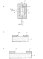
図1は、一実施形態による成膜方法を用いて、基体上に薄膜である金属膜をリフトオフによって成膜した状態を示し、図1(a)は基体上面から見た模式図、図1(b)は同図(a)のA−A’線の矢視1における模式断面図、図1(c)は同図(a)のB−B’線の矢視2における模式断面図、図1(d)は同図(a)のC−C’線の矢視3における模式断面図である。 FIG. 1 shows a state in which a metal film, which is a thin film, is formed on a substrate by lift-off using the film forming method according to one embodiment, and FIG. 1 (a) is a schematic view seen from the upper surface of the substrate. b) is a schematic cross-sectional view taken along the line AA ′ in FIG. 1A, and FIG. 1C is a schematic cross-sectional view taken along the line BB ′ in FIG. 1 (d) is a schematic cross-sectional view taken along the line CC ′ in FIG.
本実施形態における金属膜は、図1(b)〜(d)に示す模式断面図からわかるように、金属膜11の全周において、端部にいくにつれて膜厚が漸減する形状をとる。詳細については図2の説明で述べる。さらに、形成された金属膜に角があると、角の部分から剥がれやすい。そこで、本実施形態においては、図1(a)に示すように、基体上の金属膜が形成された形成面における金属膜11は、角にアール(丸み)がつくよう金属膜11が形成されている。つまり、基体10の上面から金属膜11をみると、角がない形状になっている。これは、リフトオフ成膜において、犠牲層であるAlパターンの角にアールをつけることで対応できる。
As can be seen from the schematic cross-sectional views shown in FIGS. 1B to 1D, the metal film in the present embodiment has a shape in which the film thickness gradually decreases toward the end on the entire circumference of the
このように本実施形態においては、金属膜11の全体において剥がれにくい構造にしたことで、信頼性の高い金属膜の形成が可能となる。
As described above, in the present embodiment, since the
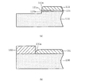
図2(a)に、本実施形態における金属膜11の端縁部の断面形状を拡大して示す。金属膜11は、中央部の目標膜厚から膜端に行くにつれてほぼ実質的に膜厚が略ゼロになるまで、公知のcosine lawにしたがって膜厚が漸減する端縁部11aを有し、また、図2(b)に示すように、基体10と金属膜11の間に密着層21が介在する場合は、端縁部11aが密着層21の膜端21aを覆うように形成される。密着層21にはいわゆる反応性のよい材料、例えばTi、Cr、NiまたはTaなどが好適に使われるが、本実施形態においては密着層の端部が金属膜11の端縁部11aに覆われているため、密着層が各種薬剤に溶解したり、酸化等の反応を起したりして損傷してしまうことを防ぐことが可能となる。
FIG. 2A shows an enlarged cross-sectional shape of the edge portion of the
上述のような膜厚が漸減する端縁部11aを有する金属膜11は、図2(c)に示すように、側面に逆テーパー部12aによるオーバーハングを有する犠牲層であるAlパターン12を用いたリフトオフ成膜によって成膜される。
As shown in FIG. 2C, the
すなわち、スパッタリングでは基体に成膜粒子が入射する方向の角度分布があり、上記の端縁部11aを形成するために、Alパターン12の側面に成膜粒子を付着させないように、側面が入射方向に対して影になるような逆テーパー部12aを有する断面形状にすればよい。リフトオフ成膜の代わりに、Alパターン12と同様の断面形状のマスクを用いたマスク成膜を採用することもできる。
That is, in the sputtering, there is an angle distribution in the direction in which the film forming particles are incident on the substrate, and in order to form the
Alパターン12の逆テーパー部12aのテーパー角は、破線で示す成膜粒子の入射角の最大値より大きく設定される。入射角によるスパッタ粒子量の分布は、ターゲットからの距離、コリメータ、成膜パワーなど、装置や成膜条件によって異なる。
The taper angle of the
Siウエハなどの基体10に対して、側面が逆テーパー形状のAlパターン12のテーパー角が成膜粒子の入射角の最大値よりも大きいため、Alパターン12の開口部から入射する成膜粒子が基体10に当る領域の外端すなわち成膜端部(膜端)は、Alパターン12の開口端より外側になり、スパッタ直後は、図3(a)に示すように、基体10の露出面に金属膜11、Alパターン12上に金属膜13が堆積している。
Since the taper angle of the
ここで、図5に金属膜が形成される過程の模式図を示す。金属膜11−1、金属膜11−2、金属膜11−3、は、時間がたつにつれて金属膜が形成されていく様子を示している。このように、形成途中の膜も端縁部がcosine lawにしたがって膜厚が漸減する形状をとっているため、膜の形成中においても膜内の応力が発生しにくい。 Here, FIG. 5 shows a schematic diagram of the process of forming the metal film. The metal film 11-1, the metal film 11-2, and the metal film 11-3 show how the metal film is formed over time. Thus, since the film in the middle of formation also has a shape in which the film thickness gradually decreases in accordance with cosine law, stress in the film hardly occurs even during film formation.
犠牲層としては、図3(b)に示すように、逆テーパー形状の代わりに段差22aによるオーバーハングを有するAlパターン22を用いてもよい。Alパターン12、22上の金属膜13は、Alパターン12、22をエッチングすることによって除去される。このようにして、膜端に向かってほぼ実質的に膜厚が0になるまで漸減する端縁部11aを備えた金属膜11を成膜することができる。
As the sacrificial layer, as shown in FIG. 3B, an
図2(b)に示すように密着層21を持つ場合は、同図(c)に示すAlパターン12を有する基体10上に、予めTi、Crなどの密着性を向上させる材料をスパッタして密着層21を形成し、引き続き金属膜11となる膜材料をより厚く上層にスパッタすることで、cosine lawによる膜厚分布を有する金属膜11が密着層21を覆った構成の2層膜を得ることができる。
When the
図7に、上述の金属膜を形成する犠牲層の概略図を示す。図7(a)は基体上面から見た概略図、図7(b)は図7(a)のA−A’線の矢視1における概略断面図、図7(c)は図7(a)のB−B’線の矢視2における概略断面図を示す。 FIG. 7 shows a schematic diagram of a sacrificial layer for forming the above metal film. 7A is a schematic view seen from the top surface of the substrate, FIG. 7B is a schematic cross-sectional view taken along line AA ′ of FIG. 7A, and FIG. 7C is FIG. ) Is a schematic cross-sectional view taken along line BB ′ of FIG.
このように、形成する金属膜全周において端縁部がcosine lawにしたがって膜厚が漸減するように、犠牲層にオーバーハング12aを設け、さらに、基体上面から見た犠牲層の角にアールをつけることで、図1(a)に示すように金属膜11の角にもアールがつき、金属膜11の全体において剥がれにくい構造にすることができる。
As described above, the sacrificial layer is provided with the
このように膜端に行くにしたがってほぼ実質的に膜厚が0になるまで漸減する端縁部を有する金属膜は、逆テーパー部や段差によるオーバーハングを有するマスクによるマスク成膜でも得られる。しかしマスクと基体のアライメントや加熱成膜時の歪み、熱膨張の違いによる位置ずれなどをマスクの材質や工程の最適化によって補償しても、マスク自体が厚いため、成膜のエッジ位置精度の点で、Alパターン等の無機レジストによるリフトオフの方が優れている。 In this way, the metal film having the edge portion that gradually decreases until the film thickness becomes substantially zero as it goes to the film end can be obtained by mask film formation using a mask having an inverse taper portion or an overhang due to a step. However, even if the alignment between the mask and the substrate, distortion during heating film formation, or misalignment due to differences in thermal expansion is compensated by optimizing the mask material and process, the mask itself is thick, so the edge position accuracy of the film formation In this respect, lift-off using an inorganic resist such as an Al pattern is superior.
リフトオフ成膜に用いる、金属等の無機レジストの犠牲層の形成は以下の手順で行われる。犠牲層は、逆テーパー形状等によるオーバーハングを有し、以下の手順で形成される。 Formation of a sacrificial layer of an inorganic resist such as a metal used for lift-off film formation is performed according to the following procedure. The sacrificial layer has an overhang due to a reverse tapered shape or the like, and is formed by the following procedure.
(1)基体に、同一エッチャントについて、エッチングレートの速い材料による下層と、比較して遅い材料による上層を有する多層構造を形成する。
(2)その上に、上記エッチャントに耐性のあるレジストをパターニングする。
(3)上記エッチャントでエッチングを行う。下層の方がエッチングが速いので、逆テーパー形状等によるオーバーハングが形成される。
(1) A multilayer structure having a lower layer made of a material having a high etching rate and an upper layer made of a material slower than the same etchant is formed on the substrate.
(2) A resist resisting the above etchant is patterned thereon.
(3) Etching is performed with the above etchant. Since etching is faster in the lower layer, an overhang due to an inverted taper shape or the like is formed.
まず、Alターゲットを用いて、Arのスパッタガスに酸素を導入しながらリアクティブスパッタした酸化アルミ膜の、混酸(リン酸:酢酸:硝酸:水=15:1:1:1、40℃)に対するエッチングレートを測定した結果を図4のグラフに示す。このグラフから、酸素の導入量が増加するに従ってエッチングレートが大きくなり、10%程度で最大値になることがわかる。 First, with respect to a mixed acid (phosphoric acid: acetic acid: nitric acid: water = 15: 1: 1: 1, 40 ° C.) of an aluminum oxide film reactively sputtered while introducing oxygen into an Ar sputtering gas using an Al target. The results of measuring the etching rate are shown in the graph of FIG. From this graph, it can be seen that the etching rate increases as the amount of oxygen introduced increases, and reaches a maximum value at about 10%.
そこで、図8(a)に示すように、Siウエハを基体として、下層に酸素10%導入による酸化アルミ層12bを約300nm形成した。引き続き図8(b)に示すように、Arスパッタガスのみで上層のAl層12cを約300nm成膜した。次に図8(c)に示すように、その上にフォトレジストを1〜2μm塗布しパターニングしてレジストパターン16を形成した。さらに上記混酸にて、エッチングを行い、目視にてAl層がなくなりSiウエハの基体表面が見えてから30秒オーバーエッチングを行った。
Therefore, as shown in FIG. 8A, an
このサンプル図8(d)の断面をSEMにて観察したところ、逆テーパー形状のAlパターン12であることが確認できた。なお、オーバーエッチング時間を変えるとテーパー角の調整ができることも確認した。
When the cross section of this sample FIG. 8D was observed with an SEM, it was confirmed that the
上記の工程により、Siウエハからなる基体上にAlパターンを作成し、密着層としてTi膜を10nm成膜し、その上に金属膜であるIr膜を200nm成膜した。 Through the above steps, an Al pattern was formed on a substrate made of a Si wafer, a Ti film was formed to a thickness of 10 nm as an adhesion layer, and an Ir film as a metal film was formed to a thickness of 200 nm thereon.
その断面をSEMにて観察したところ、犠牲層であるAlパターンの側面に膜は付着せず、Ir膜の端部には、ほぼ膜厚が0になるまで、図2に示すように漸減する端縁部が形成されていることが確認できた。 When the cross section was observed with an SEM, the film did not adhere to the side surface of the Al pattern, which is the sacrificial layer, and gradually decreased as shown in FIG. It was confirmed that an edge portion was formed.
このように作成したものを、混酸浸漬により、Alパターンの大きさとエッチングレートから決まる時間だけエッチングし、純水洗浄後、リンスシャワー乾燥機で洗浄乾燥した。 The product thus prepared was etched by mixed acid immersion for a time determined by the size of the Al pattern and the etching rate, washed with pure water, and then washed and dried with a rinse shower dryer.
その状態で観察すると、脱落すべきAlパターンや不要なIr層が恐らく水による吸着で基体から離れないものがあったため、密着テープ(エレップホルダーV−8M(商品名、日東電工株式会社製)を基体に貼り付けて剥がしたところ、全て除去できた。他に超音波洗浄などの手段でも除去できることを確認したが、Siウエハへの力のかかりが少ない密着による剥離の方が優れている。 When observed in that state, there was an Al pattern that should be removed and an unnecessary Ir layer that probably did not separate from the substrate due to water adsorption, so an adhesive tape (ELEP Holder V-8M (trade name, manufactured by Nitto Denko Corporation) It was confirmed that it could be removed by other means such as ultrasonic cleaning, but peeling by adhesion with less force applied to the Si wafer was superior.
また、逆テーパーの適切な量については、以下のようなことがわかった。オーバーエッチングが少なすぎると、逆テーパー角が小さくなり、犠牲層であるAlパターンの側面に成膜粒子が付着し始める。その状態でリフトオフをすると、犠牲層上の膜と基体に形成した膜がつながり除去が難しくなる、また、膜端が厚みを持つので、引張力が充分に緩和できない、さらには、Ti膜である密着層が表面に露出して耐食性が劣る等の問題が発生する。逆に、オーバーエッチングが多すぎると犠牲層パターンのオーバーハングが薄く長くなるために、オーバーハングの先端が基体に垂れ下がり、成膜された膜が犠牲層パターンと基体をつないでしまうのでリフトオフができなくなる。 Moreover, the following things were understood about the suitable amount of reverse taper. If the over-etching is too small, the reverse taper angle becomes small, and the deposited particles start to adhere to the side surface of the Al pattern that is the sacrificial layer. If lift-off is performed in this state, the film on the sacrificial layer and the film formed on the substrate are connected and difficult to remove, and since the film edge has a thickness, the tensile force cannot be sufficiently relaxed. Further, it is a Ti film. The adhesion layer is exposed on the surface, causing problems such as poor corrosion resistance. Conversely, if the overetching is too much, the overhang of the sacrificial layer pattern becomes thin and long, so that the tip of the overhang hangs down on the substrate, and the deposited film connects the sacrificial layer pattern and the substrate. Disappear.
インクなどの液体を吐出口から吐出して被プリント材上に画素を形成する液体吐出記録方式に用いられる液体吐出ヘッドの耐久保護膜に本発明を適用した例を示す。 An example in which the present invention is applied to a durable protective film of a liquid discharge head used in a liquid discharge recording method in which a liquid such as ink is discharged from a discharge port to form pixels on a print material will be described.
図9に液体吐出ヘッド70の一部断面部を有する概略図を示す。
FIG. 9 is a schematic view having a partial cross-section of the
Si等の基板に、エネルギー発生体として、発熱体であるヒータ74が配置されている。Si基板上の天板79にはインク室73と吐出口76がヒータ74にそれぞれ対応して設けられている。インクは、Si基板に設けられた細長いインク供給口75からインク室73に供給され、ヒータ74によって、吐出口76から吐出される。
A
液体吐出ヘッドの耐久保護膜は、耐食性、密着性とも優れていることを必要とする。図10に示すような膜構造を有する液体吐出ヘッドの耐久性を評価した。 The durable protective film of the liquid discharge head needs to have excellent corrosion resistance and adhesion. The durability of the liquid discharge head having the film structure as shown in FIG. 10 was evaluated.
図10は、液体吐出ヘッドの吐出エネルギー発生体を有する素子基板の膜構成を示すもので、素子基板の断面図を示す。この基板の製作工程は以下の通りである。下地の蓄熱層を有するSiウエハからなる基体51の上にTaN膜の発熱抵抗体52とAl膜の配線導体53を順次スパッタする。次いで、フォトリソグラフィとエッチングによって配線である配線パターンとエネルギー発生部である発熱抵抗体パターンを形成し、その後、絶縁保護膜である第1の保護膜となるSiN膜54をCVDにより形成した後、密着層21をTiで形成し、耐久保護膜である第2の保護膜となるIrの金属膜55をリフトオフによって成膜した。すなわち、耐キャビテーション性等を必要とするエネルギー発生部のみを覆う第2の保護膜としてIrの金属膜55をパターン成膜した。密着層21の端部は、金属膜55の膜厚が略ゼロになるまで膜厚が漸減する端縁部によって覆われているため、密着層が各種薬剤に溶解したり、酸化等の反応を起したりして損傷してしまうことを防ぐことが可能となる。
FIG. 10 shows a film configuration of an element substrate having a discharge energy generator of a liquid discharge head, and shows a cross-sectional view of the element substrate. The manufacturing process of this substrate is as follows. A
従来例のように第2の保護膜としてTa膜を用いる場合は、塩素系ガスによるドライエッチングをする。そして、電気配線の外部引き出し端子として用いるAlパッド部の絶縁層と第2の保護膜をドライエッチングで取り去る。このようにTaを第2の保護膜に使用した場合は、塩素系ガスを用いて化学的にエッチングすることができるが、Ir等の貴金属は化学的に安定なため、エッチングが難しい。そこで、図10に示す膜構成の液体吐出ヘッドにおいて、以下の方法で金属膜55であるIr膜のパターン成膜を行った。
When a Ta film is used as the second protective film as in the conventional example, dry etching using a chlorine-based gas is performed. Then, the insulating layer of the Al pad portion used as the external lead terminal of the electrical wiring and the second protective film are removed by dry etching. Thus, when Ta is used for the second protective film, it can be chemically etched using a chlorine-based gas. However, etching is difficult because noble metals such as Ir are chemically stable. Therefore, in the liquid discharge head having the film configuration shown in FIG. 10, the Ir film as the
サンプルA、B、Cに分けて液体吐出ヘッドを10個ずつ製作した。まず、第1の保護膜であるSiN膜上に、犠牲層の下層として酸素10%導入の酸化アルミ層を約300nm、引き続きArスパッタガスのみでAlの上層を約300nm成膜し、その上にフォトレジストを1〜2μm塗布しパターニングしてレジストパターンを形成した。さらに混酸(リン酸:酢酸:硝酸:水=15:1:1:1、40℃)にて、エッチングを行い、サンプルAは30秒、サンプルBは60秒、サンプルCは90秒のオーバーエッチングを行い、断面形状の異なるAlパターンを形成した。レジスト剥離液でフォトレジストを剥離後、密着層の形成として、まず基体を逆スパッタ後、成膜圧力5×10⁻¹Pa、基体温度300℃、パワー300WでTi膜を10nm成膜し、つづいて耐久保護層である第2の保護層として、成膜圧力7×10⁻¹Pa、基体温度300℃、パワー1000WでIr膜を200nm成膜した。その後、混酸でリフトオフを行い、純水洗浄、シャワーリンス乾燥後、密着テープ(エレップホルダーV−8M(商品名、日東電工株式会社製)を貼り付けて、リフトオフ後に基体表面に張りついているIr膜を除去した。以降、公知の吐出手段であるインク室や吐出口が形成される天板等を形成して、各サンプルごとに液体吐出ヘッドを10個ずつ作成した。 Ten liquid discharge heads were manufactured for each of Samples A, B, and C. First, on the SiN film which is the first protective film, an aluminum oxide layer introduced with 10% oxygen as a lower layer of a sacrificial layer is formed to about 300 nm, and subsequently an upper layer of Al is formed to about 300 nm using only Ar sputtering gas. A photoresist was applied by 1-2 μm and patterned to form a resist pattern. Further, etching is performed with a mixed acid (phosphoric acid: acetic acid: nitric acid: water = 15: 1: 1: 1, 40 ° C.), sample A is 30 seconds, sample B is 60 seconds, and sample C is 90 seconds. Then, Al patterns having different cross-sectional shapes were formed. After stripping the photoresist with a resist stripper, the adhesion layer is formed by first reverse sputtering the substrate, and then depositing a 10 nm Ti film at a deposition pressure of 5 × 10 −1 Pa, a substrate temperature of 300 ° C., and a power of 300 W. As a second protective layer, which is a durable protective layer, an Ir film having a thickness of 200 nm was formed at a film forming pressure of 7 × 10 −1 Pa, a substrate temperature of 300 ° C., and a power of 1000 W. Then, lift-off with mixed acid, pure water cleaning, shower rinse drying, adhesive tape (ELEP Holder V-8M (trade name, manufactured by Nitto Denko Corporation) is pasted, and Ir that sticks to the substrate surface after lift-off. Thereafter, an ink chamber, which is a known ejection means, a top plate on which ejection ports are formed, and the like were formed, and 10 liquid ejection heads were prepared for each sample.
比較のためのサンプルDとして、SiN膜を形成した後、犠牲層をつけずにサンプルA〜Cと同じ条件で、Ti膜を10nm、Ir膜を200nm成膜した。その後、フォトレジストでパターンを形成し、ミーリング装置でスパッタエッチングを行い、引き続きインク室や吐出口の形成などの諸工程を経て液体吐出ヘッドを10個作成した。 As a sample D for comparison, after forming a SiN film, a Ti film was formed to a thickness of 10 nm and an Ir film was formed to a thickness of 200 nm under the same conditions as the samples A to C without a sacrificial layer. After that, a pattern was formed with a photoresist, sputter etching was performed with a milling apparatus, and 10 liquid ejection heads were formed through various processes such as formation of ink chambers and ejection openings.
また、比較のためのサンプルEとして、SiN膜を形成した後、0.2mm厚の42Niで密着マスクを製作し、マスク成膜を行った。精度の問題で両面からのエッチングによりマスクを製作したため、逆テーパーは形成できなかった。 Further, as a sample E for comparison, after forming a SiN film, an adhesion mask was manufactured with 42 Ni having a thickness of 0.2 mm, and a mask film was formed. Since the mask was manufactured by etching from both sides due to the problem of accuracy, a reverse taper could not be formed.
マスク密着後、サンプルA〜Cと同じ条件でTi膜を10nm、Ir膜を200nm成膜した。その後、インク室や吐出口の形成などの諸工程を経て液体吐出ヘッドを10個作成した。 After the mask contact, a Ti film of 10 nm and an Ir film of 200 nm were formed under the same conditions as Samples A to C. Thereafter, ten liquid discharge heads were formed through various processes such as formation of ink chambers and discharge ports.
膜質、密着性の不具合は耐久性に反映すると考えて、ヒータである発熱抵抗体に、発泡電圧測定と、駆動周波数10kHz、パルス幅1μsec、駆動電圧を発泡電圧×1.3の駆動条件で5×10⁸ パルスの発泡耐久試験を行った結果、リフトオフで作成したサンプルA〜Cはすべて耐久テストをクリアーしたが、スパッタエッチングによるサンプルDのうちの4個、マスク成膜で作成したサンプルEのうちの2個は、発泡しなくなったものがあった。 It is assumed that defects in film quality and adhesiveness are reflected in durability, and a heating resistor as a heater is subjected to foaming voltage measurement, a driving frequency of 10 kHz, a pulse width of 1 μsec, and a driving voltage of 5 under a driving condition of foaming voltage × 1.3. As a result of conducting a foaming endurance test of × 10 8 pulses, all the samples A to C created by lift-off cleared the endurance test, but four of the samples D by sputter etching and the sample E created by mask film formation Two of them no longer foamed.

スパッタエッチングによるサンプルDで発泡しなくなった4個のうち2個は、ヒータが切れておらず、断面を観察したところ、第1の保護膜と第2の保護膜の間で剥離を起していることがわかった。また、密着層のTi膜は識別できなかった。残り2個はヒータの破断を伴っており、第2の保護膜も一部無くなっていた。また、マスク成膜したサンプルEで発泡しなくなった2個は、ヒータの破断を伴っており、第2の保護膜も一部無くなっていた。 Of the four samples that no longer foamed in the sample D by sputter etching, the heater was not cut and the cross section was observed, and peeling occurred between the first protective film and the second protective film. I found out. Further, the Ti film of the adhesion layer could not be identified. The remaining two were accompanied by breakage of the heater, and part of the second protective film was also lost. In addition, two of the samples E in which the mask was formed no longer foamed were accompanied by breakage of the heater, and part of the second protective film was also lost.
その原因として推定されるのは、Ti膜が浸食されて密着力が弱かったため、もしくは、引張力が大きくかかったために、第2の保護膜が剥がれたと考えられる。また、スパッタエッチングが選択比がないために、第1の保護膜もある程度エッチングしたことなどから、第1の保護膜からインクが浸透しヒータを損傷したことが考えられる。 The reason is presumably that the second protective film was peeled off because the Ti film was eroded and the adhesion was weak or the tensile force was large. In addition, since the sputter etching has no selectivity, the first protective film was also etched to some extent, and it is considered that ink penetrated from the first protective film and damaged the heater.
マスク成膜、スパッタエッチングいずれにしても、製法としてはリフトオフの方が耐久性がよかったのは端縁部における形状的な要素が大きいと考えられ、犠牲層を使ったリフトオフの優位性が確認できた。 In both mask deposition and sputter etching, the lift-off process was more durable because the shape factor at the edge was larger, and the superiority of lift-off using a sacrificial layer could be confirmed. It was.
このように、エッチングレートの異なる多層膜構成のAlパターンを使ったリフトオフによって成膜することで、密着性のよいIr膜を得ることができる。そして、このようなIr等の貴金属膜を素子基板の保護層として用いることで、耐久性能のよい液体吐出ヘッドを実現できる。 As described above, an Ir film having good adhesion can be obtained by forming the film by lift-off using an Al pattern having a multilayer film structure with different etching rates. By using such a noble metal film such as Ir as a protective layer of the element substrate, a liquid discharge head with good durability can be realized.
エッチングレートの異なるAlの多層膜の成膜において、Alの酸素のリアクティブスパッタの代わりに、窒素のリアクティブスパッタを用いてもよい。また、金属はAlに限定されず、Cr、Cu、Mo等酸化物や窒化物を形成できる金属材料ならば、エッチャントを選ぶことで同様の効果を得ることができる。また、Al等無機材料の犠牲層は高温成膜に耐えるので、Ir以外の貴金属、例えばPt(白金)、Os(オスミウム)、Ru(ルテニウム)またはNi(ニッケル)などのパターン成膜に適用できる。また、これらの材料は密着を必要とすることが多いので、上記形状の端縁部によって密着層を全面的に覆う構成は特に有効である。 In forming Al multilayer films having different etching rates, nitrogen reactive sputtering may be used instead of Al oxygen reactive sputtering. Further, the metal is not limited to Al, and a similar effect can be obtained by selecting an etchant as long as it is a metal material that can form oxides and nitrides such as Cr, Cu, and Mo. In addition, since a sacrificial layer of an inorganic material such as Al can withstand high-temperature film formation, it can be applied to pattern film formation of noble metals other than Ir, such as Pt (platinum), Os (osmium), Ru (ruthenium), or Ni (nickel). . In addition, since these materials often require close contact, a configuration in which the close contact layer is entirely covered with the edge portion having the above shape is particularly effective.
本実施例においては、液体を吐出するために利用されるエネルギーを発生するエネルギー発生体として発熱抵抗体を利用し、インク等の液体に熱エネルギーを与えることで気泡を発生させ、該気泡の形成によって液体を吐出させる方式の例を示したが、エネルギー発生体として圧電素子を利用したものにも適用可能である。 In this embodiment, a heating resistor is used as an energy generator that generates energy used to discharge liquid, and bubbles are generated by applying thermal energy to a liquid such as ink, thereby forming the bubbles. Although an example of a method of discharging a liquid by the above is shown, it is also applicable to a method using a piezoelectric element as an energy generator.
さらに、本発明は、上述のように凹部に金属膜を形成する際のみならず、図6に示すように、基体10の凸部15上に金属膜11を形成した場合においても、端部にいくにつれて膜厚を薄くし、さらに上述したように角にアールをつけるように金属膜を形成することで、剥がれにくく信頼性の高い金属膜の形成が可能となる。このように、本発明の成膜方法は、液体吐出ヘッドの素子基板上の薄膜に限定されることなく、各種半導体素子、エレクトロニクス素子等の基板上の薄膜に適用できる。
Furthermore, in the present invention, not only when the metal film is formed in the concave portion as described above, but also when the
10、51 基体
11、55 金属膜
11a 端縁部
12、22 Alパターン
12a 逆テーパー部
21 密着層
22a 段差
52 発熱抵抗体
53 配線導体
54 SiN膜
DESCRIPTION OF
Claims (8)
オーバーハングを有する犠牲層が形成された基体に前記膜の材料を堆積させる工程と、
前記犠牲層を除去することによって、前記犠牲層と前記犠牲層上に堆積した前記膜の材料とを除去する工程と、を有することを特徴とする成膜方法。 A film forming method for forming a film on a substrate,
Depositing the material of the film on a substrate on which a sacrificial layer having an overhang is formed;
Removing the sacrificial layer to remove the sacrificial layer and the material of the film deposited on the sacrificial layer.
前記基体側から、酸素および窒素の少なくとも一方を含む金属化合物の下層と、
前記下層の上に、前記下層より低い濃度の酸素および窒素の少なくとも一方を含む金属化合物または金属の上層と、を備えることを特徴とする請求項1に記載の成膜方法。 The sacrificial layer is
From the base side, a lower layer of a metal compound containing at least one of oxygen and nitrogen,
The film forming method according to claim 1, further comprising a metal compound or metal upper layer including at least one of oxygen and nitrogen having a lower concentration than the lower layer on the lower layer.
前記膜が、所定膜厚を有する中央部と、前記所定膜厚から膜端において膜厚が略ゼロになるまで漸減する膜厚分布を有する端縁部と、を備えていることを特徴とする基板。 A substrate comprising a film and a substrate formed by the film forming method according to claim 1 or 2,
The film includes a central portion having a predetermined film thickness, and an edge portion having a film thickness distribution that gradually decreases from the predetermined film thickness until the film thickness becomes substantially zero at the film edge. substrate.
前記膜の前記端縁部によって前記密着層の端部が覆われていることを特徴とする請求項3または5のいずれか1項に記載の基板。 Having an adhesion layer between the substrate and the film;
The substrate according to claim 3, wherein an end portion of the adhesion layer is covered with the edge portion of the film.
前記エネルギー発生体に接続された配線と、
前記エネルギー発生体および前記配線を覆う絶縁保護膜と、
前記絶縁保護膜上に選択的に設けられた耐久保護膜とを有し、
前記耐久保護膜が、請求項1または2に記載の成膜方法によって形成された膜であることを特徴とする液体吐出ヘッド。 An energy generator that generates energy used to discharge the liquid;
Wiring connected to the energy generator;
An insulating protective film covering the energy generator and the wiring;
A durable protective film selectively provided on the insulating protective film,
The liquid discharge head according to claim 1, wherein the durable protective film is a film formed by the film forming method according to claim 1.
前記エネルギー発生体に接続された配線と、
前記エネルギー発生体および前記配線を覆う絶縁保護膜と、
前記絶縁保護膜上に設けられた密着層と、
前記密着層上に設けられた耐久保護膜と、を有し、
前記耐久保護膜は、所定膜厚を有する中央部と、前記所定膜厚から膜端において膜厚が略ゼロになるまで漸減する膜厚分布を有する端縁部とを備え、
前記端縁部によって前記密着層の端部が覆われていることを特徴とする液体吐出ヘッド。 An energy generator that generates energy used to discharge the liquid provided on the substrate;
Wiring connected to the energy generator;
An insulating protective film covering the energy generator and the wiring;
An adhesion layer provided on the insulating protective film;
A durable protective film provided on the adhesion layer,
The durable protective film comprises a central portion having a predetermined film thickness, and an edge portion having a film thickness distribution that gradually decreases from the predetermined film thickness until the film thickness is substantially zero at the film end,
An end portion of the adhesion layer is covered with the end edge portion.
Priority Applications (1)
| Application Number | Priority Date | Filing Date | Title |
|---|---|---|---|
| JP2005074231A JP2005314802A (en) | 2004-03-31 | 2005-03-16 | Film-forming method, base plate and liquid discharge head |
Applications Claiming Priority (2)
| Application Number | Priority Date | Filing Date | Title |
|---|---|---|---|
| JP2004101842 | 2004-03-31 | ||
| JP2005074231A JP2005314802A (en) | 2004-03-31 | 2005-03-16 | Film-forming method, base plate and liquid discharge head |
Publications (2)
| Publication Number | Publication Date |
|---|---|
| JP2005314802A true JP2005314802A (en) | 2005-11-10 |
| JP2005314802A5 JP2005314802A5 (en) | 2006-02-02 |
Family
ID=35442520
Family Applications (1)
| Application Number | Title | Priority Date | Filing Date |
|---|---|---|---|
| JP2005074231A Pending JP2005314802A (en) | 2004-03-31 | 2005-03-16 | Film-forming method, base plate and liquid discharge head |
Country Status (1)
| Country | Link |
|---|---|
| JP (1) | JP2005314802A (en) |
Cited By (12)
| Publication number | Priority date | Publication date | Assignee | Title |
|---|---|---|---|---|
| JP2008105364A (en) * | 2005-12-09 | 2008-05-08 | Canon Inc | Substrate for inkjet head, inkjet head with substrate, cleaning method for inkjet head, and inkjet recorder using inkjet head |
| JP2010032298A (en) * | 2008-07-28 | 2010-02-12 | Toshiba Corp | Scintillator panel |
| US7795144B2 (en) | 2007-06-06 | 2010-09-14 | Sony Corporation | Method for forming electrode structure for use in light emitting device and method for forming stacked structure |
| JP2010208237A (en) * | 2009-03-11 | 2010-09-24 | Seiko Epson Corp | Liquid jetting head, liquid jetting apparatus, and actuator |
| JP2012101557A (en) * | 2005-12-09 | 2012-05-31 | Canon Inc | Inkjet head and inkjet recording device |
| JP2012121262A (en) * | 2010-12-09 | 2012-06-28 | Ricoh Co Ltd | Ink-jet apparatus |
| JP2012201025A (en) * | 2011-03-25 | 2012-10-22 | Ngk Insulators Ltd | Flow passage part |
| JP2013021187A (en) * | 2011-07-12 | 2013-01-31 | Mitsubishi Electric Corp | Mim capacitor and manufacturing method therefor, and semiconductor device |
| DE102014221915A1 (en) | 2013-10-28 | 2015-04-30 | Hamamatsu Photonics K.K. | Quantum Cascade Lasers |
| JP2016038280A (en) * | 2014-08-07 | 2016-03-22 | コニカミノルタ株式会社 | Scintillator panel and radioactive-ray detector including the same |
| JP2017002338A (en) * | 2015-06-05 | 2017-01-05 | 旭硝子株式会社 | Optical member and method for manufacturing optical member |
| CN110699671A (en) * | 2019-10-21 | 2020-01-17 | 江苏菲沃泰纳米科技有限公司 | Coating clamp and application thereof |
-
2005
- 2005-03-16 JP JP2005074231A patent/JP2005314802A/en active Pending
Cited By (16)
| Publication number | Priority date | Publication date | Assignee | Title |
|---|---|---|---|---|
| US8491087B2 (en) | 2005-12-09 | 2013-07-23 | Canon Kabushiki Kaisha | Circuit board for ink jet head, ink jet head having the same, method for cleaning the head and ink jet printing apparatus using the head |
| US8123330B2 (en) | 2005-12-09 | 2012-02-28 | Canon Kabushiki Kaisha | Circuit board for ink jet head, ink jet head having the same, method for cleaning the head and ink jet printing apparatus using the head |
| JP2012101557A (en) * | 2005-12-09 | 2012-05-31 | Canon Inc | Inkjet head and inkjet recording device |
| JP2008105364A (en) * | 2005-12-09 | 2008-05-08 | Canon Inc | Substrate for inkjet head, inkjet head with substrate, cleaning method for inkjet head, and inkjet recorder using inkjet head |
| US7795144B2 (en) | 2007-06-06 | 2010-09-14 | Sony Corporation | Method for forming electrode structure for use in light emitting device and method for forming stacked structure |
| JP2010032298A (en) * | 2008-07-28 | 2010-02-12 | Toshiba Corp | Scintillator panel |
| JP2010208237A (en) * | 2009-03-11 | 2010-09-24 | Seiko Epson Corp | Liquid jetting head, liquid jetting apparatus, and actuator |
| JP2012121262A (en) * | 2010-12-09 | 2012-06-28 | Ricoh Co Ltd | Ink-jet apparatus |
| JP2012201025A (en) * | 2011-03-25 | 2012-10-22 | Ngk Insulators Ltd | Flow passage part |
| JP2013021187A (en) * | 2011-07-12 | 2013-01-31 | Mitsubishi Electric Corp | Mim capacitor and manufacturing method therefor, and semiconductor device |
| DE102014221915A1 (en) | 2013-10-28 | 2015-04-30 | Hamamatsu Photonics K.K. | Quantum Cascade Lasers |
| US9276381B2 (en) | 2013-10-28 | 2016-03-01 | Hamamatsu Photonics K.K. | Quantum cascade laser |
| DE102014221915B4 (en) | 2013-10-28 | 2023-12-28 | Hamamatsu Photonics K.K. | Quantum cascade laser |
| JP2016038280A (en) * | 2014-08-07 | 2016-03-22 | コニカミノルタ株式会社 | Scintillator panel and radioactive-ray detector including the same |
| JP2017002338A (en) * | 2015-06-05 | 2017-01-05 | 旭硝子株式会社 | Optical member and method for manufacturing optical member |
| CN110699671A (en) * | 2019-10-21 | 2020-01-17 | 江苏菲沃泰纳米科技有限公司 | Coating clamp and application thereof |
Similar Documents
| Publication | Publication Date | Title |
|---|---|---|
| JP2005314802A (en) | Film-forming method, base plate and liquid discharge head | |
| KR100846348B1 (en) | Method of manufacturing substrate for ink jet recording head and method of manufacturing recording head using substrate manufactured by this method | |
| US4777494A (en) | Process for manufacturing an electrothermal transducer for a liquid jet recording head by anodic oxidation of exposed portions of the transducer | |
| US4889587A (en) | Method of preparing a substrate for ink jet head and method of preparing an ink jet head | |
| JP2844051B2 (en) | Thermal head | |
| US20030156161A1 (en) | Monolithic printhead with self-aligned groove and relative manufacturing process | |
| US20200189275A1 (en) | Liquid ejection head and a manufacturing method of the same | |
| US7677696B2 (en) | Liquid discharge head | |
| JP5328608B2 (en) | Substrate for liquid discharge head, liquid discharge head and manufacturing method thereof | |
| JP5008448B2 (en) | Method for manufacturing substrate for ink jet recording head | |
| JP2013173262A (en) | Method for manufacturing liquid ejection head | |
| JP3041601B2 (en) | Manufacturing method of thermal head | |
| JP5224929B2 (en) | Manufacturing method of liquid discharge recording head | |
| US6808641B2 (en) | Method of wiring formation and method for manufacturing electronic components | |
| JP6921698B2 (en) | Liquid discharge head and its manufacturing method | |
| JP6643911B2 (en) | Liquid discharge head substrate, liquid discharge head, liquid discharge device, and method of manufacturing liquid discharge head substrate | |
| JP4235420B2 (en) | Substrate processing method | |
| JP2019181723A (en) | Substrate for liquid discharge head and method of manufacturing the same, and liquid discharge head | |
| JP2006225745A (en) | Structure of thin film element and method for producing the same | |
| JP2006224590A (en) | Method for manufacturing inkjet recording head | |
| JP2007245639A (en) | Manufacturing method of inkjet recording head | |
| JP2009006503A (en) | Substrate for inkjet recording head and its manufacturing method | |
| JP7172398B2 (en) | Inkjet head manufacturing method | |
| JP3397532B2 (en) | Base for liquid jet recording head and method of manufacturing the same | |
| JPH09118018A (en) | Manufacture of ink-jet recording head substrate |
Legal Events
| Date | Code | Title | Description |
|---|---|---|---|
| A521 | Written amendment |
Effective date: 20051212 Free format text: JAPANESE INTERMEDIATE CODE: A523 |
|
| A621 | Written request for application examination |
Free format text: JAPANESE INTERMEDIATE CODE: A621 Effective date: 20051212 |
|
| A977 | Report on retrieval |
Free format text: JAPANESE INTERMEDIATE CODE: A971007 Effective date: 20080717 |
|
| A131 | Notification of reasons for refusal |
Free format text: JAPANESE INTERMEDIATE CODE: A131 Effective date: 20080729 |
|
| A521 | Written amendment |
Free format text: JAPANESE INTERMEDIATE CODE: A523 Effective date: 20080929 |
|
| A131 | Notification of reasons for refusal |
Effective date: 20090210 Free format text: JAPANESE INTERMEDIATE CODE: A131 |
|
| A521 | Written amendment |
Effective date: 20090410 Free format text: JAPANESE INTERMEDIATE CODE: A523 |
|
| RD03 | Notification of appointment of power of attorney |
Free format text: JAPANESE INTERMEDIATE CODE: A7423 Effective date: 20090527 |
|
| A02 | Decision of refusal |
Effective date: 20090924 Free format text: JAPANESE INTERMEDIATE CODE: A02 |