JP2005311306A - Vertical-type heat treating apparatus and workpiece transfer method - Google Patents
Vertical-type heat treating apparatus and workpiece transfer method Download PDFInfo
- Publication number
- JP2005311306A JP2005311306A JP2005055271A JP2005055271A JP2005311306A JP 2005311306 A JP2005311306 A JP 2005311306A JP 2005055271 A JP2005055271 A JP 2005055271A JP 2005055271 A JP2005055271 A JP 2005055271A JP 2005311306 A JP2005311306 A JP 2005311306A
- Authority
- JP
- Japan
- Prior art keywords
- substrate support
- processed
- heat treatment
- holder
- transfer
- Prior art date
- Legal status (The legal status is an assumption and is not a legal conclusion. Google has not performed a legal analysis and makes no representation as to the accuracy of the status listed.)
- Pending
Links
Images


Classifications
-
- H—ELECTRICITY
- H01—ELECTRIC ELEMENTS
- H01L—SEMICONDUCTOR DEVICES NOT COVERED BY CLASS H10
- H01L21/00—Processes or apparatus adapted for the manufacture or treatment of semiconductor or solid state devices or of parts thereof
- H01L21/67—Apparatus specially adapted for handling semiconductor or electric solid state devices during manufacture or treatment thereof; Apparatus specially adapted for handling wafers during manufacture or treatment of semiconductor or electric solid state devices or components ; Apparatus not specifically provided for elsewhere
- H01L21/677—Apparatus specially adapted for handling semiconductor or electric solid state devices during manufacture or treatment thereof; Apparatus specially adapted for handling wafers during manufacture or treatment of semiconductor or electric solid state devices or components ; Apparatus not specifically provided for elsewhere for conveying, e.g. between different workstations
- H01L21/67739—Apparatus specially adapted for handling semiconductor or electric solid state devices during manufacture or treatment thereof; Apparatus specially adapted for handling wafers during manufacture or treatment of semiconductor or electric solid state devices or components ; Apparatus not specifically provided for elsewhere for conveying, e.g. between different workstations into and out of processing chamber
- H01L21/67757—Apparatus specially adapted for handling semiconductor or electric solid state devices during manufacture or treatment thereof; Apparatus specially adapted for handling wafers during manufacture or treatment of semiconductor or electric solid state devices or components ; Apparatus not specifically provided for elsewhere for conveying, e.g. between different workstations into and out of processing chamber vertical transfer of a batch of workpieces
-
- B—PERFORMING OPERATIONS; TRANSPORTING
- B65—CONVEYING; PACKING; STORING; HANDLING THIN OR FILAMENTARY MATERIAL
- B65G—TRANSPORT OR STORAGE DEVICES, e.g. CONVEYORS FOR LOADING OR TIPPING, SHOP CONVEYOR SYSTEMS OR PNEUMATIC TUBE CONVEYORS
- B65G49/00—Conveying systems characterised by their application for specified purposes not otherwise provided for
- B65G49/05—Conveying systems characterised by their application for specified purposes not otherwise provided for for fragile or damageable materials or articles
- B65G49/07—Conveying systems characterised by their application for specified purposes not otherwise provided for for fragile or damageable materials or articles for semiconductor wafers Not used, see H01L21/677
-
- F—MECHANICAL ENGINEERING; LIGHTING; HEATING; WEAPONS; BLASTING
- F27—FURNACES; KILNS; OVENS; RETORTS
- F27B—FURNACES, KILNS, OVENS, OR RETORTS IN GENERAL; OPEN SINTERING OR LIKE APPARATUS
- F27B17/00—Furnaces of a kind not covered by any preceding group
- F27B17/0016—Chamber type furnaces
- F27B17/0025—Especially adapted for treating semiconductor wafers
-
- F—MECHANICAL ENGINEERING; LIGHTING; HEATING; WEAPONS; BLASTING
- F27—FURNACES; KILNS; OVENS; RETORTS
- F27B—FURNACES, KILNS, OVENS, OR RETORTS IN GENERAL; OPEN SINTERING OR LIKE APPARATUS
- F27B5/00—Muffle furnaces; Retort furnaces; Other furnaces in which the charge is held completely isolated
- F27B5/04—Muffle furnaces; Retort furnaces; Other furnaces in which the charge is held completely isolated adapted for treating the charge in vacuum or special atmosphere
-
- F—MECHANICAL ENGINEERING; LIGHTING; HEATING; WEAPONS; BLASTING
- F27—FURNACES; KILNS; OVENS; RETORTS
- F27B—FURNACES, KILNS, OVENS, OR RETORTS IN GENERAL; OPEN SINTERING OR LIKE APPARATUS
- F27B5/00—Muffle furnaces; Retort furnaces; Other furnaces in which the charge is held completely isolated
- F27B5/06—Details, accessories, or equipment peculiar to furnaces of these types
- F27B5/12—Arrangement of devices for charging
-
- F—MECHANICAL ENGINEERING; LIGHTING; HEATING; WEAPONS; BLASTING
- F27—FURNACES; KILNS; OVENS; RETORTS
- F27B—FURNACES, KILNS, OVENS, OR RETORTS IN GENERAL; OPEN SINTERING OR LIKE APPARATUS
- F27B5/00—Muffle furnaces; Retort furnaces; Other furnaces in which the charge is held completely isolated
- F27B5/06—Details, accessories, or equipment peculiar to furnaces of these types
- F27B5/13—Arrangement of devices for discharging
-
- F—MECHANICAL ENGINEERING; LIGHTING; HEATING; WEAPONS; BLASTING
- F27—FURNACES; KILNS; OVENS; RETORTS
- F27D—DETAILS OR ACCESSORIES OF FURNACES, KILNS, OVENS, OR RETORTS, IN SO FAR AS THEY ARE OF KINDS OCCURRING IN MORE THAN ONE KIND OF FURNACE
- F27D3/00—Charging; Discharging; Manipulation of charge
- F27D3/12—Travelling or movable supports or containers for the charge
-
- H—ELECTRICITY
- H01—ELECTRIC ELEMENTS
- H01L—SEMICONDUCTOR DEVICES NOT COVERED BY CLASS H10
- H01L21/00—Processes or apparatus adapted for the manufacture or treatment of semiconductor or solid state devices or of parts thereof
- H01L21/67—Apparatus specially adapted for handling semiconductor or electric solid state devices during manufacture or treatment thereof; Apparatus specially adapted for handling wafers during manufacture or treatment of semiconductor or electric solid state devices or components ; Apparatus not specifically provided for elsewhere
- H01L21/677—Apparatus specially adapted for handling semiconductor or electric solid state devices during manufacture or treatment thereof; Apparatus specially adapted for handling wafers during manufacture or treatment of semiconductor or electric solid state devices or components ; Apparatus not specifically provided for elsewhere for conveying, e.g. between different workstations
- H01L21/67763—Apparatus specially adapted for handling semiconductor or electric solid state devices during manufacture or treatment thereof; Apparatus specially adapted for handling wafers during manufacture or treatment of semiconductor or electric solid state devices or components ; Apparatus not specifically provided for elsewhere for conveying, e.g. between different workstations the wafers being stored in a carrier, involving loading and unloading
- H01L21/67778—Apparatus specially adapted for handling semiconductor or electric solid state devices during manufacture or treatment thereof; Apparatus specially adapted for handling wafers during manufacture or treatment of semiconductor or electric solid state devices or components ; Apparatus not specifically provided for elsewhere for conveying, e.g. between different workstations the wafers being stored in a carrier, involving loading and unloading involving loading and unloading of wafers
- H01L21/67781—Batch transfer of wafers
-
- H—ELECTRICITY
- H01—ELECTRIC ELEMENTS
- H01L—SEMICONDUCTOR DEVICES NOT COVERED BY CLASS H10
- H01L21/00—Processes or apparatus adapted for the manufacture or treatment of semiconductor or solid state devices or of parts thereof
- H01L21/67—Apparatus specially adapted for handling semiconductor or electric solid state devices during manufacture or treatment thereof; Apparatus specially adapted for handling wafers during manufacture or treatment of semiconductor or electric solid state devices or components ; Apparatus not specifically provided for elsewhere
- H01L21/683—Apparatus specially adapted for handling semiconductor or electric solid state devices during manufacture or treatment thereof; Apparatus specially adapted for handling wafers during manufacture or treatment of semiconductor or electric solid state devices or components ; Apparatus not specifically provided for elsewhere for supporting or gripping
- H01L21/687—Apparatus specially adapted for handling semiconductor or electric solid state devices during manufacture or treatment thereof; Apparatus specially adapted for handling wafers during manufacture or treatment of semiconductor or electric solid state devices or components ; Apparatus not specifically provided for elsewhere for supporting or gripping using mechanical means, e.g. chucks, clamps or pinches
- H01L21/68707—Apparatus specially adapted for handling semiconductor or electric solid state devices during manufacture or treatment thereof; Apparatus specially adapted for handling wafers during manufacture or treatment of semiconductor or electric solid state devices or components ; Apparatus not specifically provided for elsewhere for supporting or gripping using mechanical means, e.g. chucks, clamps or pinches the wafers being placed on a robot blade, or gripped by a gripper for conveyance
Abstract
Description
本発明は、縦型熱処理装置及び被処理体移載方法に係り、特にリング状支持板を有する保持具に対して被処理体を複数枚ずつ移載可能に移載機構の構造を改良した縦型熱処理装置及び被処理体移載方法に関する。 The present invention relates to a vertical heat treatment apparatus and a method for transferring an object to be processed, and more particularly, an improved vertical structure in which a plurality of objects to be processed can be transferred to a holder having a ring-shaped support plate. The present invention relates to a mold heat treatment apparatus and an object transfer method.
半導体装置の製造においては、被処理体例えば半導体ウエハに例えば酸化、拡散、CVD、アニール等の各種の熱処理を施す工程があり、これらの工程を実行するための熱処理装置の一つとして多数枚のウエハを一度に熱処理することが可能な縦型熱処理装置が用いられている。 In the manufacture of semiconductor devices, there are processes for subjecting an object to be processed, such as a semiconductor wafer, to various heat treatments such as oxidation, diffusion, CVD, annealing, etc. A vertical heat treatment apparatus capable of heat treating a wafer at a time is used.
この縦型熱処理装置は、下部に炉口を有する熱処理炉と、その炉口を密閉する蓋体と、この蓋体上に設けられ多数枚のウエハをリング状支持板を介して上下方向に所定間隔で保持する保持具(ウエハボートともいう)と、前記蓋体を昇降させて保持具を熱処理炉に搬入搬出する昇降機構と、複数枚のウエハを所定間隔で収納する収納容器(キャリア、カセットともいう)と前記保持具との間でウエハの移載を行う複数枚の基板支持具(フォークともいう)を所定間隔で有する移載機構とを備えている。前記リング状支持板は高温熱処理時にウエハの周縁部に発生するスリップ(結晶欠陥)を抑制ないし防止する対策として用いられている。 This vertical heat treatment apparatus includes a heat treatment furnace having a furnace port at the bottom, a lid for sealing the furnace port, and a plurality of wafers provided on the lid in a vertical direction via a ring-shaped support plate. A holding tool (also called a wafer boat) that holds at intervals, an elevating mechanism that raises and lowers the lid and carries the holding tool into and out of the heat treatment furnace, and a storage container (carrier, cassette) that stores a plurality of wafers at predetermined intervals And a transfer mechanism having a plurality of substrate supports (also referred to as forks) for transferring the wafer between the holder and the holder. The ring-shaped support plate is used as a measure for suppressing or preventing slip (crystal defects) generated at the peripheral edge of the wafer during high-temperature heat treatment.
前記移載機構としては、図12に示すように移載用基板支持具50と、突き上げ用基板支持具51とを備えた突き上げ式の移載機構(移載機構Aという)が用いられている(例えば特開平5−13547号公報参照)。移載用基板支持具50はウエハwの下面と対接する上面を有する板状体からなり、突き上げ用基板支持具51はその上面にウエハwの下面と対接する3本の支持ピン52を有する板状体からなる。
As the transfer mechanism, as shown in FIG. 12, a push-up type transfer mechanism (referred to as transfer mechanism A) provided with a
ウエハを保持具に移載する場合、先ずウエハwを支持した移載用基板支持具50を保持具9内の所定のリング状支持板15の上方に挿入すると共に、突き上げ用基板支持具51を前記リング状支持板15の下方に挿入する〔図12の(a)〕。次に、突き上げ用基板支持具51を上昇させて移載用基板支持具50上からウエハwを持ち上げ、この状態で移載用基板支持具50を保持具9から退去させる〔図12の(b)〕。次に、突き上げ用基板支持具51を下降させてウエハwをリング状支持板15上に支持させた後、突き上げ用基板支持具51を保持具9から退去させることにより1枚のウエハの移載作業が完了するようになっている〔図12の(c)〕。
When transferring a wafer to a holder, first, a transfer substrate support 50 that supports the wafer w is inserted above a predetermined ring-
なお、移載機構としては、ウエハ周縁部における下側面に係止してウエハを吊下げ状態で支持する複数の係止部材を備え、各係止部材が、ウエハを吊下げ状態で支持するウエハ支持位置と、ウエハの外形周縁の外側まで移動してウエハの支持状態を解除するウエハ解除位置との間で往復移動できるように構成されると共に、各係止部材が、ウエハ支持位置とウエハ解除位置の範囲でアクチュエータにより往復駆動されるように構成されているもの(移載機構Bという)が知られている(特開2003−338531号公報)。 The transfer mechanism includes a plurality of engaging members that are engaged with the lower surface of the peripheral edge of the wafer to support the wafer in a suspended state, and each engaging member supports the wafer in a suspended state. It is configured to be able to reciprocate between the support position and the wafer release position that moves to the outside of the outer peripheral edge of the wafer and releases the support state of the wafer, and each locking member has the wafer support position and the wafer release position. A device that is reciprocally driven by an actuator within a range of positions (referred to as a transfer mechanism B) is known (Japanese Patent Application Laid-Open No. 2003-338531).
しかしながら、従来の縦型熱処理装置においては、いずれの移載機構A,Bも、ウエハを1枚ずつしか移載することができないため、移載時間が多くかかるという問題がある。また、移載機構の構造上、保持具のリング状支持板間のピッチを大きく(16mm程度)必要とし、保持具に搭載し得るウエハの枚数(処理枚数)は最大50枚程度が限界であり、スループットの低下を余儀なくされていた。特に、移載機構Bの場合、フォーク(基板支持具)の先端側及び後端側に配置した係止部材がいずれも可動する構造であるため、構造の複雑化及び肉厚寸法の増大を招き、保持具のリング状支持板間のピッチを小さくすることが難しい。 However, in the conventional vertical heat treatment apparatus, any of the transfer mechanisms A and B can transfer only one wafer at a time. Also, due to the structure of the transfer mechanism, the pitch between the ring-shaped support plates of the holder is required to be large (about 16 mm), and the maximum number of wafers (number of processed sheets) that can be mounted on the holder is about 50. Was forced to reduce the throughput. In particular, in the case of the transfer mechanism B, since the locking members arranged on the front end side and the rear end side of the fork (substrate support) are both movable, the structure is complicated and the wall thickness is increased. It is difficult to reduce the pitch between the ring-shaped support plates of the holder.
本発明は、上記事情を考慮してなされたものであり、リング状支持板を有する保持具に対して被処理体を複数枚ずつ移載することができ、移載時間の短縮、処理枚数の増大及びスループットの向上が図れる縦型熱処理装置及び被処理体移載方法を提供することを目的とする。 The present invention has been made in consideration of the above circumstances, and can transfer a plurality of objects to be processed to a holder having a ring-shaped support plate one by one, shortening the transfer time and the number of processed sheets. It is an object of the present invention to provide a vertical heat treatment apparatus and a method for transferring an object to be processed that can increase and improve throughput.
本発明のうち、請求項1の発明は、下部に炉口を有する熱処理炉と、その炉口を密閉する蓋体と、該蓋体上に設けられ多数枚の被処理体をリング状支持板を介して上下方向に所定間隔で保持する保持具と、前記蓋体を昇降させて保持具を熱処理炉に搬入搬出する昇降機構と、複数枚の被処理体を所定間隔で収納する収納容器と前記保持具との間で被処理体の移載を行う複数枚の基板支持具を所定間隔で有する移載機構とを備え、該移載機構の各基板支持具下に被処理体を上掴みする上掴み機構を設け、該上掴み機構は基板支持具の先端部に設けられ被処理体の前縁部を係止する固定係止部と、基板支持具の後端側に設けられ被処理体の後縁部を着脱可能に係止する可動係止部とを有していることを特徴とする。
Among the present inventions, the invention of
請求項2の発明は、前記基板支持具には該基板支持具の下面と被処理体の上面との間に隙間を存するように被処理体の前後周縁部を受ける受け部が設けられていることを特徴とする。 According to a second aspect of the present invention, the substrate support is provided with a receiving portion for receiving the front and rear peripheral edges of the object to be processed so that a gap exists between the lower surface of the substrate support and the upper surface of the object to be processed. It is characterized by that.
請求項3の発明は、前記リング状支持板には前記固定係止部及び可動係止部との干渉を避けるための切欠部が設けられていることを特徴とする。 The invention according to claim 3 is characterized in that the ring-shaped support plate is provided with a notch for avoiding interference with the fixed locking portion and the movable locking portion.
請求項4の発明は、前記基板支持具の先端部にはその両側間に張られた光線を遮るように基板支持具を移動させることにより被処理体の位置を検出するマッピングセンサが設けられていることを特徴とする。 According to a fourth aspect of the present invention, a mapping sensor that detects the position of the object to be processed by moving the substrate support so as to block the light beam stretched between both sides is provided at the tip of the substrate support. It is characterized by being.
請求項5の発明は、前記固定係止部及び可動係止部が耐熱性樹脂材からなっていることを特徴とする。
The invention according to
請求項6の発明は、下部に炉口を有する熱処理炉と、その炉口を密閉する蓋体と、該蓋体上に設けられ多数枚の被処理体をリング状支持板を介して上下方向に所定間隔で保持する保持具と、前記蓋体を昇降させて保持具を熱処理炉に搬入搬出する昇降機構と、複数枚の被処理体を所定間隔で収納する収納容器と前記保持具との間で被処理体の移載を行うための複数枚の基板支持具を所定間隔で有する移載機構とを備え、該移載機構の各基板支持具下に被処理体を上掴みする上掴み機構を設け、該上掴み機構は基板支持具の先端部に設けられ被処理体の前縁部を係止する固定係止部と、基板支持具の後端側に設けられ被処理体の後縁部を着脱可能に係止する可動係止部とを有する縦型熱処理装置における被処理体の移載方法であって、前記移載機構の各基板支持具下に設けた上掴み機構により被処理体を上掴みして前記移載を行うことを特徴とする。
The invention according to
本発明のうちの請求項1の発明によれば、前記移載機構が複数枚の各基板支持具下に被処理体を上掴みする上掴み機構を具備しているため、リング状支持板を有する保持具に対して被処理体を複数枚ずつ移載することができ、移載時間の短縮化が図れる。特に、前記上掴み機構が、基板支持具の先端部に設けられ被処理体の前縁部を係止する固定係止部と、基板支持具の後端側に設けられ被処理体の後縁部を着脱可能に係止する可動係止部とを有しているため、構造の簡素化が図れ、これにより保持具のリング状支持板間のピッチを小さくすることができて処理枚数の増大が図れ、もってスループットの向上が図れる。 According to the first aspect of the present invention, since the transfer mechanism includes an upper gripping mechanism for gripping an object to be processed under each of the plurality of substrate supports, the ring-shaped support plate is It is possible to transfer a plurality of objects to be processed to the holding tool, and to shorten the transfer time. In particular, the upper gripping mechanism is provided at the front end portion of the substrate support tool and locks the front edge portion of the target object, and the rear edge of the target object provided at the rear end side of the substrate support tool. Since it has a movable locking part that detachably locks the part, the structure can be simplified, and the pitch between the ring-shaped support plates of the holder can be reduced, thereby increasing the number of processed sheets. As a result, throughput can be improved.
請求項2の発明によれば、前記基板支持具には該基板支持具の下面と被処理体の上面との間に隙間を存するように被処理体の前後周縁部を受ける受け部が設けられているため、被処理体を上掴みする際に基板支持具の下面で被処理体の上面を擦って傷付けるのを防止することができる。 According to invention of Claim 2, the said board | substrate support tool is provided with the receiving part which receives the front-and-back periphery part of a to-be-processed object so that a clearance gap may exist between the lower surface of this substrate support tool, and the upper surface of a to-be-processed object. Therefore, it is possible to prevent the upper surface of the target object from being rubbed and damaged by the lower surface of the substrate support when the target object is gripped.
請求項3の発明によれば、前記リング状支持板には前記固定係止部及び可動係止部との干渉を避けるための切欠部が設けられているため、上掴み機構がリング状支持板と干渉することなく被処理体を確実に上掴みすることができる。 According to the invention of claim 3, since the ring-shaped support plate is provided with a notch for avoiding interference with the fixed locking portion and the movable locking portion, the upper gripping mechanism is the ring-shaped support plate. It is possible to reliably grasp the object to be processed without interfering with the object.
請求項4の発明によれば、前記基板支持具の先端部にはその両側間に張られた光線を遮るように基板支持具を移動させることにより被処理体の位置を検出するマッピングセンサが設けられているため、保持具内に多段に保持された被処理体に沿って上下方向に走査することにより保持具内における被処理体の有無を検出して位置情報として記録(マッピング)することができると共に、処理前後の被処理体の飛び出しの有無を検出して被処理体の破損等の事故を未然に防止することができる。 According to a fourth aspect of the present invention, a mapping sensor that detects the position of the object to be processed by moving the substrate support so as to block the light beam stretched between both sides thereof is provided at the tip of the substrate support. Therefore, the presence / absence of the object to be processed in the holder can be detected by scanning in the vertical direction along the object to be processed held in multiple stages in the holder, and can be recorded (mapped) as position information. In addition, it is possible to prevent an accident such as breakage of the object to be processed by detecting the presence or absence of the object to be processed before and after the process.
請求項5の発明によれば、前記固定係止部及び可動係止部が耐熱性樹脂材からなっているため、耐久性の向上が図れると共に被処理体の汚染源にならない。
According to invention of
請求項6の発明によれば、前記移載機構の各基板支持具下に設けた上掴み機構により被処理体を上掴みして前記移載を行うため、移載時間の短縮化が図れると共に、保持具のリング状支持板間のピッチを小さくして処理枚数の増大が図れ、もってスループットの向上が図れる。
According to the invention of
以下に、本発明を実施するための最良の形態について、添付図面を基に詳述する。図1は本発明の実施の形態である縦型熱処理装置を概略的に示す縦断面図、図2は移載機構を示す図、図3は図2の同移載機構を一側から見た図、図4は移載機構の要部を示す図、図5はリング状支持板の一例を示す図である。 The best mode for carrying out the present invention will be described below in detail with reference to the accompanying drawings. 1 is a longitudinal sectional view schematically showing a vertical heat treatment apparatus according to an embodiment of the present invention, FIG. 2 is a view showing a transfer mechanism, and FIG. 3 is a view of the transfer mechanism of FIG. 2 from one side. FIG. 4 is a diagram showing a main part of the transfer mechanism, and FIG. 5 is a diagram showing an example of a ring-shaped support plate.
図1に示すように、この縦型熱処理装置1は外郭を形成する筐体2を有し、この筐体2内の上方に被処理体(被処理基板ともいう)例えば薄板円板状の半導体ウエハwを収容して所定の処理例えばCVD処理等を施すための縦型の熱処理炉3が設けられている。この熱処理炉3は、下部が炉口4として開口された縦長の処理容器例えば石英製の反応管5と、この反応管5の炉口4を開閉する昇降可能な蓋体6と、前記反応管5の周囲を覆うように設けられ、反応管5内を所定の温度例えば300〜1200℃に加熱制御可能なヒータ(加熱機構)7とから主に構成されている。
As shown in FIG. 1, the vertical
前記筐体2内には、熱処理炉3を構成する反応管5やヒータ7を設置するための例えばSUS製のベースプレート8が水平に設けられている。ベースプレート8には反応管5を下方から上方に挿入するための図示しない開口部が形成されている。
In the housing 2, for example, a
反応管5の下端部には外向きのフランジ部が形成され、このフランジ部をフランジ保持部材にてベースプレート8に保持することにより、反応管5がベースプレート8の開口部を下方から上方に挿通された状態に設置されている。反応管5は、洗浄等のためにベースプレート8から下方に取外せるようになっている。反応管5には反応管5内に処理ガスやパージ用の不活性ガスを導入する複数のガス導入管や反応管5内を減圧制御可能な真空ポンプや圧力制御弁等を有する排気管が接続されている(図示省略)。
An outward flange portion is formed at the lower end of the
前記筐体2内におけるベースプレート8より下方には、蓋体6上に設けられた保持具(ボート)9を熱処理炉3(すなわち反応管5)内に搬入(ロード)したり、熱処理炉3から搬出(アンロード)したり、或いは保持具9に対するウエハwの移載を行うための作業領域(ローディングエリア)10が設けられている。この作業領域10にはボート9の搬入、搬出を行うべく蓋体6を昇降させるための昇降機構11が設けられている。蓋体6は炉口4の開口端に当接して炉口4を密閉するように構成されている。蓋体6の下部には保持具を回転するための図示しない回転機構が設けられている。
Below the
図示例の保持具9は、例えば石英製であり、大口径例えば直径300mmの多数例えば75枚程度のウエハwをリング状支持板15を介して水平状態で上下方向に所定間隔例えば11mmピッチで多段に支持する本体部9aと、この本体部9aを支持する脚部9bとを備え、脚部9bが回転機構の回転軸に接続されている。本体部9aと蓋体6との間には炉口4からの放熱による温度低下を防止するための図示しない下部加熱機構が設けられている。なお、保持具9としては、本体部9aのみを有し、脚部9bを有せず、蓋体6上に保温筒を介して載置されるものであってもよい。前記保持具9は複数本の支柱12と、この支柱12の上端及び下端に設けられた天板13及び底板14と、支柱12に所定間隔で設けられた凹部又は凸部に係合させて多段に配置されたリング状支持板15と備えている。リング状支持板15は、例えば石英製又はセラミック製であり、厚さが2〜3mm程度であり、ウエハwの外径よりも若干大きい外径に形成されている。
The
筐体2の前部には、複数例えば25枚程度のウエハを所定間隔で収納した収納容器(キャリア、カセットともいう)16を載置して筐体2内への搬入搬出を行うための載置台(ロードポート)17が設置されている。収納容器16は前面に図示しない蓋を着脱可能に備えた密閉型収納容器とされている。作業領域10内の前後には収納容器16の蓋を取外して収納容器内を作業領域10内に連通開放するドア機構18が設けられ、作業領域10には収納容器16と保持具9の間でウエハwの移載を行う複数枚の基板支持具(フォーク)20を所定間隔で有する移載機構21が設けられている。
A storage container (also referred to as a carrier or a cassette) 16 that stores a plurality of, for example, about 25 wafers at a predetermined interval is placed on the front portion of the housing 2 for loading / unloading into / from the housing 2. A stand (load port) 17 is installed. The
作業領域10外の前部上側には、収納容器16をストックしておくための保管棚部22と、載置台17から保管棚部22へ又はその逆に収納容器16を搬送するための図示しない搬送機構とが設けられている。なお、作業領域10の上方には蓋体6を開けた時に炉口4から高温の炉内の熱が下方の作業領域10に放出されるのを抑制ないし防止するために炉口4を覆う(又は塞ぐ)シャッター機構23が設けられている。
On the front upper side outside the
前記移載機構21は、複数枚例えば5枚のウエハwを上下方向に所定間隔で支持する複数枚例えば5枚の基板支持具(支持板)20(20a〜20e)を有している。この場合、中央の基板支持具20aは単独で前方に進退移動可能とされ、中央以外の基板支持具(一枚目、二枚目、四枚目及び五枚目)20b,20c,20d,20eは図示しないピッチ変換機構により中央の基板支持具20aを基準として上下方向に無段階でピッチ変換可能とされている。これは、収納容器16内のウエハの収納ピッチと、保持具9内のウエハの搭載ピッチとが異なる場合があるので、その場合でも収納容器16と保持具9との間でウエハwを複数枚ずつ移載可能とするためである。
The
移載機構21は、昇降可能な昇降アーム24と、この昇降アーム24に水平旋回可能に設けられた箱型の基台25とを有し、この基台25上には中央の1枚の基板支持具20aを前方へ移動可能とする第1の移動体26と、中央の基板支持具20aを挟んで上下に2枚ずつ配された計4枚の基板支持具20b〜20eを前方へ移動可能とする第2の移動体27とが基台25の長手方向に沿って進退移動可能に設けられている。これにより、第1の移動体26の単独動により1枚のウエハを移載する枚葉移載と、第1及び第2の移動体26,27の共動により複数枚例えば5枚のウエハを同時に移載する一括移載とを選択的に行えるようになっている。第1及び第2の移動体26,27を移動操作するために、基台25の内部には図示しない移動機構が設けられている。この移動機構及び前記ピッチ変換機構は、例えば特開2001−44260号公報に記載のものが用いられている。
The
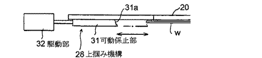
基板支持具20は例えばアルミナセラミックにより縦長薄板状に形成されている。基板支持具20は先端が二股に分岐された平面略U字状に形成されていることが好ましい(図4,図6,図7参照)。移載機構21は、各基板支持具20下にウエハwを一枚ずつ上掴みすることが可能な上掴み機構28を具備している。この上掴み機構28は、図8〜図10にも示すように基板支持具20の先端部に設けられウエハwの前縁部を係止する固定係止部30と、基板支持具20の後端側に設けられウエハwの後縁部を着脱可能に係止する可動係止部31と、この可動係止部31を駆動する駆動部例えばエアシリンダ32とを備えている。
The
エアシリンダ32で可動係止部31を前進させることにより固定係止部30との間でウエハwを前後から挟む(掴む)ことができ、可動係止部31を後退させることによりウエハwを解放することができるようになっている。基板支持具20の基端部には可動係止部31との干渉を避けるための切欠部33が設けられていることが好ましい。
By moving the
固定係止部30及び可動係止部31はウエハwの周縁部を自重で離脱しないように支えるために傾斜面30a、31aを有していることが好ましい。また、前記基板支持具20には該基板支持具20の下面とウエハwの上面との間に隙間gを存するようにウエハwの前後周縁部を受けるスぺーサとしての受け部34,35が設けられていることが好ましい。図示例の場合、前部の受け部34と後部の受け部35が左右2個ずつ設けられている。また、前部の受け部34と前記固定係止部30が一体的に形成されており、コンパクト化が図られている。固定係止部30、可動係止部31、受け部34,35の材質としては、耐熱性樹脂材例えばPEEK(Poly Ether Ether Ketone)材が耐久性の向上が図れると共にウエハの汚染源にならない点で好ましい。
The fixed
前記リング状支持板15においては、ウエハwよりも外径が大きい場合には、図4ないし図5に示すように前記固定係止部30及び可動係止部31、場合によっては基部側の受け部35との干渉を避けるための切欠部36,37が設けられていることが好ましい。なお、リング状支持板15は、ウエハwよりも外径が小さい場合には、必ずしも切欠部36,37を設ける必要はない。
When the outer diameter of the ring-shaped
上下のリング状支持板15,15間の隙間に1枚の基板支持具20を挿入し得るように、前記基板支持具20の上面と前部の固定係止部30の下面との間の厚さ寸法hは、上部のリング状支持板15の下面と下部のリング状支持板15上のウエハw上面との間の隙間寸法k(7.7mm程度)よりも小さい寸法例えば5.95mm程度に形成されていることが好ましい。なお、枚葉移載が可能な基板支持具20aの先端部には、例えば移載機構21のティーチング作業時にマッピングを行うためのマッピングセンサ40が設けられている。
Thickness between the upper surface of the
図示例では、基板支持具20の一方の先端部に赤外光線の出入光が可能なマッピングセンサ40のセンサヘッド40aが設けられ、他方の先端部にはマッピングセンサ40のセンサヘッド40aから出光された赤外光線を反射させてマッピングセンサ40のセンサヘッド40aに入光させる反射鏡41が設けられており、移載機構21のティーチング移動時に被検出物により赤外光線が遮られることによりその被検出物の位置を検出できるようになっている。図示例のマッピングセンサ40は、センサヘッド40aと図示しない検出機構側の発光素子及び受光素子を光ファイバ42で接続して構成されている。移載機構21は、図5に示すように前記マッピングセンサ40を、保持具9内に多段に保持されたウエハwに沿って上下方向(図5の紙面垂直方向)に走査することにより、保持具9内の各段におけるウエハwの有無を検出して位置情報として記録(マッピング)することができると共に、処理前後のウエハwの状態(例えば飛び出しの有無)を検出可能に構成されている。
In the illustrated example, a
基板支持具20の一方の先端部には赤外光線の出光及び入光が可能なマッピングセンサヘッド40が設けられ、他方の先端部にはマッピングセンサヘッド40から出光された赤外光線を反射させてマッピングセンサヘッド40に入光させる反射鏡41が設けられており、移載機構21のティーチング移動時に被検出物により赤外光線が遮られることによりその被検出物の位置を検出できるようになっている。マッピングセンサヘッド40には光ファイバ42を介して図示しない検出機構側の発光素子及び受光素子が接続されている。
A
以上の構成からなる縦型熱処理装置1における移載機構21の動きないし移載方法を説明すると、先ず基板支持具20を収納容器内に挿入して基板支持具20下の上掴み機構28の固定係止部30に対して可動係止部31を閉じることによりウエハwを掴み、収納容器から搬出し、この状態で基板支持具20をリング状支持板15の上方に挿入する〔図11の(a)〕。次に、上掴み機構28の固定係止部30に対して可動係止部31を開くことによりウエハwを解放してリング状支持板15上に配置する〔図11の(b)〕。次に、この状態で基板支持具20を上昇させ、更に基板支持具20を保持具9から退去させればよい〔図11の(c)〕。
The movement or transfer method of the
このように、前記縦型熱処理装置1によれば、複数枚例えば5枚の基板支持具20(20a〜20e)を有する移載機構21が各基板支持具20下にウエハwを上掴みする上掴み機構28を具備しているため、リング状支持板15を有する保持具9に対してウエハwを複数枚例えば5枚ずつ移載することができ、移載時間の大幅な短縮が図れる。特に、上掴み機構28が、基板支持具20の先端部に設けられウエハwの前縁部を係止する固定係止部30と、基板支持具20の後端側に設けられウエハ2の後縁部を着脱可能に係止する可動係止部31とからなり、基板支持具20の先端部の係止部を固定としたので、フォーク(基板支持具)の先端側及び後端側に配置した係止部材がいずれも可動である従来の移載機構Bと比べて基板支持具20の構造の簡素化及びの薄肉化が図れ、これにより保持具9のリング状支持板15間のピッチを従来の16mm程度から11mm程度に小さくして処理枚数を従来の50枚程度からその1.5倍の75枚程度に増大することができ、もってスループットの向上が図れる。
As described above, according to the vertical
また、前記上掴み機構28によりウエハwを容易に上掴みすることができる。更に、前記基板支持具20には該基板支持具20の下面とウエハwの上面との間に隙間を存するようにウエハwの前後周縁部を受ける受け部34,35が設けられているため、ウエハwを上掴みする際に基板支持具20の下面でウエハwの上面を擦って傷付けるのを防止することができる。また、前記リング状支持板15には前記固定係止部30及び可動係止部31との干渉を避けるための切欠部36,37が設けられているため、上掴み機構28がリング状支持板15と干渉することなくウエハwを確実に上掴みすることができる。
Further, the upper
前記基板支持具20の先端部にはその両側間に張られた光線を遮るように基板支持具20を移動させることにより被処理体wの位置を検出するマッピングセンサ40が設けられているため、保持具9内に多段に保持された被処理体wに沿って上下方向に走査することにより保持具9内における被処理体wの有無を検出して位置情報として記録(マッピング)することができると共に、処理前後の被処理体wの飛び出しの有無を検出して被処理体wの破損等の事故を未然に防止することができる。また、基板支持具20の先端部には固定係止部30が設けられているが、可動構造でないため互いに干渉することなくマッピングセンサ40を容易に設けることができ、基板支持具20の肉厚の増大を来たさない。
Since the tip of the
以上、本発明の実施の形態ないし実施例を図面により詳述してきたが、本発明は前記実施の形態ないし実施例に限定されるものではなく、本発明の要旨を逸脱しない範囲での種々の設計変更等が可能である。 As mentioned above, although embodiment thru | or example of this invention has been explained in full detail with drawing, this invention is not limited to the said embodiment thru | or example, Various in the range which does not deviate from the summary of this invention. Design changes can be made.
1 縦型熱処理装置
w 半導体ウエハ(被処理体)
3 熱処理炉
4 炉口
6 蓋体
9 保持具
11 昇降機構
15 リング状支持板
16 収納容器
20 基板支持具
21 移載機構
28 上掴み機構
30 固定係止部
31 可動係止部
34,35 受け部
36,37 切欠部
40 マッピングセンサ
1 Vertical heat treatment equipment w Semiconductor wafer (object to be processed)
DESCRIPTION OF SYMBOLS 3 Heat processing furnace 4
Claims (6)
A heat treatment furnace having a furnace port at the bottom, a lid for sealing the furnace port, and holding a plurality of workpieces provided on the lid in a vertical direction at predetermined intervals via a ring-shaped support plate A workpiece, an elevating mechanism that raises and lowers the lid, and loads and unloads the holder into a heat treatment furnace, and a transfer container between the holder and a storage container that stores a plurality of objects to be processed at predetermined intervals. A transfer mechanism having a plurality of substrate supports for loading at predetermined intervals, and an upper gripping mechanism for gripping an object to be processed is provided under each substrate support of the transfer mechanism. The mechanism is provided at the front end portion of the substrate support, and is fixed to the front edge portion of the object to be processed, and the rear edge portion of the object to be processed provided at the rear end side of the substrate support is detachable. A method for transferring an object to be processed in a vertical heat treatment apparatus having a movable locking portion to stop, wherein each substrate support of the transfer mechanism Workpiece transfer method comprising: performing the transfer of the object to be processed by the upper gripping mechanism provided with gripping on to.
Priority Applications (7)
| Application Number | Priority Date | Filing Date | Title |
|---|---|---|---|
| JP2005055271A JP2005311306A (en) | 2004-03-25 | 2005-03-01 | Vertical-type heat treating apparatus and workpiece transfer method |
| KR1020057022867A KR100980961B1 (en) | 2004-03-25 | 2005-03-25 | Vertical heat treatment equipment and method for transferring object to be treated |
| DE602005027689T DE602005027689D1 (en) | 2004-03-25 | 2005-03-25 | VERTICAL HEAT TREATMENT DEVICE AND METHOD FOR TRANSFERRING TREATED OBJECTS |
| EP05726958A EP1752725B1 (en) | 2004-03-25 | 2005-03-25 | Vertical heat treatment equipment and method for transferring object to be treated |
| US10/593,973 US7677858B2 (en) | 2004-03-25 | 2005-03-25 | Vertical heat treatment system and method of transferring process objects |
| PCT/JP2005/005518 WO2005093354A1 (en) | 2004-03-25 | 2005-03-25 | Vertical heat treatment equipment and method for transferring object to be treated |
| TW094109400A TW200603289A (en) | 2004-03-25 | 2005-03-25 | Vertical-type heat treating apparatus and workpiece transfer method |
Applications Claiming Priority (2)
| Application Number | Priority Date | Filing Date | Title |
|---|---|---|---|
| JP2004089515 | 2004-03-25 | ||
| JP2005055271A JP2005311306A (en) | 2004-03-25 | 2005-03-01 | Vertical-type heat treating apparatus and workpiece transfer method |
Related Child Applications (1)
| Application Number | Title | Priority Date | Filing Date |
|---|---|---|---|
| JP2008276908A Division JP2009099996A (en) | 2004-03-25 | 2008-10-28 | Vertical heat treatment system and method of transferring workpieces |
Publications (1)
| Publication Number | Publication Date |
|---|---|
| JP2005311306A true JP2005311306A (en) | 2005-11-04 |
Family
ID=35056283
Family Applications (1)
| Application Number | Title | Priority Date | Filing Date |
|---|---|---|---|
| JP2005055271A Pending JP2005311306A (en) | 2004-03-25 | 2005-03-01 | Vertical-type heat treating apparatus and workpiece transfer method |
Country Status (7)
| Country | Link |
|---|---|
| US (1) | US7677858B2 (en) |
| EP (1) | EP1752725B1 (en) |
| JP (1) | JP2005311306A (en) |
| KR (1) | KR100980961B1 (en) |
| DE (1) | DE602005027689D1 (en) |
| TW (1) | TW200603289A (en) |
| WO (1) | WO2005093354A1 (en) |
Cited By (7)
| Publication number | Priority date | Publication date | Assignee | Title |
|---|---|---|---|---|
| KR100754771B1 (en) * | 2005-12-27 | 2007-09-03 | 주식회사 엔씨비네트웍스 | Wafer Transfer having Structure for Mapping Wafer and Method for Mapping Wafer loaded in Boat thereof |
| WO2007129558A1 (en) | 2006-05-09 | 2007-11-15 | Tokyo Electron Limited | Substrate conveyance device and vertical heat treatment equipment |
| JP2009099918A (en) * | 2007-10-19 | 2009-05-07 | Tokyo Electron Ltd | Workpiece transfer mechanism, workpiece transfer method and workpiece processing system |
| JP2009231652A (en) * | 2008-03-25 | 2009-10-08 | Dainippon Screen Mfg Co Ltd | Heat treatment equipment |
| JP2010056469A (en) * | 2008-08-29 | 2010-03-11 | Tokyo Electron Ltd | Apparatus and method for heat treatment, and storage medium |
| WO2010103876A1 (en) * | 2009-03-13 | 2010-09-16 | 川崎重工業株式会社 | Robot provided with end effector, and method for operating the robot |
| JP2014207338A (en) * | 2013-04-12 | 2014-10-30 | 東京エレクトロン株式会社 | Substrate holding device, substrate processing apparatus using the same, and substrate holding method |
Families Citing this family (7)
| Publication number | Priority date | Publication date | Assignee | Title |
|---|---|---|---|---|
| JP5473857B2 (en) * | 2010-10-14 | 2014-04-16 | 東京エレクトロン株式会社 | Conveying device and processing system |
| JP5243569B2 (en) * | 2011-03-07 | 2013-07-24 | 東京エレクトロン株式会社 | Substrate transport apparatus, substrate transport method, and recording medium on which program for executing the substrate transport method is recorded |
| JP6204226B2 (en) * | 2014-02-24 | 2017-09-27 | 東京エレクトロン株式会社 | Substrate processing apparatus and substrate processing method |
| JP6468848B2 (en) * | 2015-01-13 | 2019-02-13 | 株式会社ディスコ | Transport device |
| JP6596375B2 (en) | 2016-03-31 | 2019-10-23 | 株式会社荏原製作所 | Teaching apparatus and teaching method |
| CN106382814B (en) * | 2016-11-25 | 2018-11-06 | 芜湖新兴铸管有限责任公司 | Muffle furnace annealing device |
| CN117308583B (en) * | 2023-11-24 | 2024-02-02 | 陕西三义高科石墨新材料有限公司 | Ring type roasting furnace |
Family Cites Families (21)
| Publication number | Priority date | Publication date | Assignee | Title |
|---|---|---|---|---|
| CH680275A5 (en) * | 1990-03-05 | 1992-07-31 | Tet Techno Investment Trust | |
| JP3081025B2 (en) | 1991-07-03 | 2000-08-28 | 東京エレクトロン株式会社 | Wafer transfer device |
| US5445486A (en) * | 1992-03-29 | 1995-08-29 | Tokyo Electron Sagami Limited | Substrate transferring apparatus |
| KR940006241A (en) * | 1992-06-05 | 1994-03-23 | 이노우에 아키라 | Substrate transfer device and transfer method |
| KR0152324B1 (en) * | 1994-12-06 | 1998-12-01 | 양승택 | Semiconductor wafer carrier apparatus |
| US6167322A (en) * | 1998-07-10 | 2000-12-26 | Holbrooks; Orville Ray | Intelligent wafer handling system and method |
| JP3664897B2 (en) * | 1998-11-18 | 2005-06-29 | 東京エレクトロン株式会社 | Vertical heat treatment equipment |
| JP2001267262A (en) * | 2000-03-17 | 2001-09-28 | Hitachi Kokusai Electric Inc | Semiconductor producing system |
| US20010048867A1 (en) * | 2000-03-29 | 2001-12-06 | Lebar Technology, Inc. | Method and apparatus for processing semiconductor wafers |
| JP2001284276A (en) * | 2000-03-30 | 2001-10-12 | Hitachi Kokusai Electric Inc | Substrate treating device |
| US6828772B1 (en) * | 2000-06-14 | 2004-12-07 | Micron Technology, Inc. | Rotating gripper wafer flipper |
| JP4600856B2 (en) | 2000-10-24 | 2010-12-22 | ムラテックオートメーション株式会社 | Substrate holding device |
| JP3724361B2 (en) | 2000-10-31 | 2005-12-07 | ダイキン工業株式会社 | Substrate transfer device |
| JP3939101B2 (en) * | 2000-12-04 | 2007-07-04 | 株式会社荏原製作所 | Substrate transport method and substrate transport container |
| JP2002184853A (en) * | 2000-12-15 | 2002-06-28 | Yaskawa Electric Corp | Apparatus for grasping wafer |
| JP2002289666A (en) * | 2001-03-27 | 2002-10-04 | Tokyo Electron Ltd | Heat treatment apparatus |
| JP2003007800A (en) * | 2001-06-21 | 2003-01-10 | Hitachi Kokusai Electric Inc | Substrate treatment device and method of manufacturing semiconductor device |
| US6817640B2 (en) * | 2001-06-28 | 2004-11-16 | Applied Materials, Inc. | Four-bar linkage wafer clamping mechanism |
| US7140655B2 (en) * | 2001-09-04 | 2006-11-28 | Multimetrixs Llc | Precision soft-touch gripping mechanism for flat objects |
| JP2003338531A (en) * | 2002-05-20 | 2003-11-28 | Toshiba Ceramics Co Ltd | Carrier and thermal treatment device of semiconductor wafer |
| JP2004079569A (en) | 2002-08-09 | 2004-03-11 | Sipec Corp | Substrate transport apparatus and substrate transport method |
-
2005
- 2005-03-01 JP JP2005055271A patent/JP2005311306A/en active Pending
- 2005-03-25 US US10/593,973 patent/US7677858B2/en not_active Expired - Fee Related
- 2005-03-25 WO PCT/JP2005/005518 patent/WO2005093354A1/en not_active Application Discontinuation
- 2005-03-25 DE DE602005027689T patent/DE602005027689D1/en active Active
- 2005-03-25 KR KR1020057022867A patent/KR100980961B1/en active IP Right Grant
- 2005-03-25 EP EP05726958A patent/EP1752725B1/en not_active Expired - Fee Related
- 2005-03-25 TW TW094109400A patent/TW200603289A/en not_active IP Right Cessation
Cited By (18)
| Publication number | Priority date | Publication date | Assignee | Title |
|---|---|---|---|---|
| KR100754771B1 (en) * | 2005-12-27 | 2007-09-03 | 주식회사 엔씨비네트웍스 | Wafer Transfer having Structure for Mapping Wafer and Method for Mapping Wafer loaded in Boat thereof |
| WO2007129558A1 (en) | 2006-05-09 | 2007-11-15 | Tokyo Electron Limited | Substrate conveyance device and vertical heat treatment equipment |
| US8167521B2 (en) | 2006-05-09 | 2012-05-01 | Tokyo Electron Limited | Substrate transfer apparatus and vertical heat processing apparatus |
| US8181769B2 (en) | 2007-10-19 | 2012-05-22 | Tokyo Electron Limited | Workpiece transfer mechanism, workpiece transfer method and workpiece processing system |
| JP2009099918A (en) * | 2007-10-19 | 2009-05-07 | Tokyo Electron Ltd | Workpiece transfer mechanism, workpiece transfer method and workpiece processing system |
| KR101177967B1 (en) | 2007-10-19 | 2012-08-28 | 도쿄엘렉트론가부시키가이샤 | Transfer mechanism of object to be treated, transferring method of object to be treated, treatment system of object to be treated, and storage medium storing computer readable program |
| JP2009231652A (en) * | 2008-03-25 | 2009-10-08 | Dainippon Screen Mfg Co Ltd | Heat treatment equipment |
| JP2010056469A (en) * | 2008-08-29 | 2010-03-11 | Tokyo Electron Ltd | Apparatus and method for heat treatment, and storage medium |
| US8423175B2 (en) | 2008-08-29 | 2013-04-16 | Tokyo Electron Limited | Thermal processing apparatus, thermal processing method, and storage medium |
| US8565911B2 (en) | 2008-08-29 | 2013-10-22 | Tokyo Electron Limited | Thermal processing apparatus, thermal processing method, and storage medium |
| WO2010103876A1 (en) * | 2009-03-13 | 2010-09-16 | 川崎重工業株式会社 | Robot provided with end effector, and method for operating the robot |
| JPWO2010103876A1 (en) * | 2009-03-13 | 2012-09-13 | 川崎重工業株式会社 | Robot equipped with end effector and operation method thereof |
| JP5506108B2 (en) * | 2009-03-13 | 2014-05-28 | 川崎重工業株式会社 | Robot equipped with end effector and operation method thereof |
| JP2014132684A (en) * | 2009-03-13 | 2014-07-17 | Kawasaki Heavy Ind Ltd | Robot with end effector and operation method thereof |
| JP2015167250A (en) * | 2009-03-13 | 2015-09-24 | 川崎重工業株式会社 | Robot with end effector and operation method thereof |
| US9254566B2 (en) | 2009-03-13 | 2016-02-09 | Kawasaki Jukogyo Kabushiki Kaisha | Robot having end effector and method of operating the same |
| US9616577B2 (en) | 2009-03-13 | 2017-04-11 | Kawasaki Jukogyo Kabushiki Kaisha | Robot having end effector and method of operating the same |
| JP2014207338A (en) * | 2013-04-12 | 2014-10-30 | 東京エレクトロン株式会社 | Substrate holding device, substrate processing apparatus using the same, and substrate holding method |
Also Published As
| Publication number | Publication date |
|---|---|
| US20070199860A1 (en) | 2007-08-30 |
| WO2005093354A1 (en) | 2005-10-06 |
| EP1752725B1 (en) | 2011-04-27 |
| TW200603289A (en) | 2006-01-16 |
| US7677858B2 (en) | 2010-03-16 |
| EP1752725A4 (en) | 2007-12-12 |
| TWI351723B (en) | 2011-11-01 |
| KR100980961B1 (en) | 2010-09-07 |
| EP1752725A1 (en) | 2007-02-14 |
| KR20060126857A (en) | 2006-12-11 |
| DE602005027689D1 (en) | 2011-06-09 |
Similar Documents
| Publication | Publication Date | Title |
|---|---|---|
| JP2005311306A (en) | Vertical-type heat treating apparatus and workpiece transfer method | |
| JP4313401B2 (en) | Vertical heat treatment apparatus and substrate transfer method | |
| JP4047826B2 (en) | Vertical heat treatment apparatus and automatic teaching method for transfer mechanism | |
| JP2009099996A (en) | Vertical heat treatment system and method of transferring workpieces | |
| JP4451854B2 (en) | Vertical heat treatment apparatus and control method of transfer mechanism in vertical heat treatment apparatus | |
| JP5042950B2 (en) | Vertical heat treatment apparatus and substrate support | |
| JP2007251088A (en) | Vertical heat treatment device and control method of transfer mechanism in the same | |
| JP5456287B2 (en) | Vertical heat treatment equipment | |
| WO2006043509A1 (en) | Vertical heat treatment apparatus and method for operating same | |
| JP2009099918A (en) | Workpiece transfer mechanism, workpiece transfer method and workpiece processing system | |
| TW200526496A (en) | Substrate holding tool and substrate treating device for treating semiconductor | |
| JP3543987B2 (en) | Processing equipment | |
| JP2008235810A (en) | Heat treatment method, heat treatment device, and method for transferring substrate to be treated | |
| JP2009302351A (en) | Workpiece transfer mechanism and workpiece processing system | |
| JP2002289666A (en) | Heat treatment apparatus | |
| JP4519348B2 (en) | Heat treatment apparatus and heat treatment method | |
| JP2000021784A (en) | Jig for transferring treating chamber and heater, and transferring method | |
| JP2000021801A (en) | Single-wafer heat treatment system | |
| JPH10303275A (en) | Wafer treatment device |
Legal Events
| Date | Code | Title | Description |
|---|---|---|---|
| A131 | Notification of reasons for refusal |
Free format text: JAPANESE INTERMEDIATE CODE: A131 Effective date: 20080701 |
|
| A521 | Request for written amendment filed |
Free format text: JAPANESE INTERMEDIATE CODE: A523 Effective date: 20080731 Free format text: JAPANESE INTERMEDIATE CODE: A821 Effective date: 20080731 |
|
| RD02 | Notification of acceptance of power of attorney |
Free format text: JAPANESE INTERMEDIATE CODE: A7422 Effective date: 20080731 |
|
| A02 | Decision of refusal |
Free format text: JAPANESE INTERMEDIATE CODE: A02 Effective date: 20080930 |
|
| A521 | Request for written amendment filed |
Free format text: JAPANESE INTERMEDIATE CODE: A523 Effective date: 20081028 Free format text: JAPANESE INTERMEDIATE CODE: A821 Effective date: 20081028 |
|
| A911 | Transfer to examiner for re-examination before appeal (zenchi) |
Free format text: JAPANESE INTERMEDIATE CODE: A911 Effective date: 20081203 |
|
| A912 | Re-examination (zenchi) completed and case transferred to appeal board |
Free format text: JAPANESE INTERMEDIATE CODE: A912 Effective date: 20081226 |
|
| A521 | Request for written amendment filed |
Free format text: JAPANESE INTERMEDIATE CODE: A821 Effective date: 20100204 |