JP2005295700A - Switching regulator - Google Patents
Switching regulator Download PDFInfo
- Publication number
- JP2005295700A JP2005295700A JP2004107734A JP2004107734A JP2005295700A JP 2005295700 A JP2005295700 A JP 2005295700A JP 2004107734 A JP2004107734 A JP 2004107734A JP 2004107734 A JP2004107734 A JP 2004107734A JP 2005295700 A JP2005295700 A JP 2005295700A
- Authority
- JP
- Japan
- Prior art keywords
- capacitor
- noise
- switching regulator
- filter circuit
- transformer
- Prior art date
- Legal status (The legal status is an assumption and is not a legal conclusion. Google has not performed a legal analysis and makes no representation as to the accuracy of the status listed.)
- Granted
Links
- 239000003990 capacitor Substances 0.000 claims abstract description 74
- 238000004804 winding Methods 0.000 claims abstract description 49
- 238000009499 grossing Methods 0.000 claims abstract description 34
- 239000004020 conductor Substances 0.000 claims abstract description 21
- 238000010586 diagram Methods 0.000 description 15
- 230000001603 reducing effect Effects 0.000 description 8
- 230000000694 effects Effects 0.000 description 6
- 230000005855 radiation Effects 0.000 description 6
- 230000001965 increasing effect Effects 0.000 description 5
- 239000002184 metal Substances 0.000 description 3
- 230000001939 inductive effect Effects 0.000 description 2
- 238000012986 modification Methods 0.000 description 2
- 230000004048 modification Effects 0.000 description 2
- 230000009467 reduction Effects 0.000 description 2
- OKTJSMMVPCPJKN-UHFFFAOYSA-N Carbon Chemical compound [C] OKTJSMMVPCPJKN-UHFFFAOYSA-N 0.000 description 1
- 239000006096 absorbing agent Substances 0.000 description 1
- 230000009471 action Effects 0.000 description 1
- 230000033228 biological regulation Effects 0.000 description 1
- 229910052799 carbon Inorganic materials 0.000 description 1
- 230000003247 decreasing effect Effects 0.000 description 1
- 238000005868 electrolysis reaction Methods 0.000 description 1
- 230000005284 excitation Effects 0.000 description 1
- 230000004907 flux Effects 0.000 description 1
- 230000017525 heat dissipation Effects 0.000 description 1
- 239000011810 insulating material Substances 0.000 description 1
- 238000000034 method Methods 0.000 description 1
- 230000010355 oscillation Effects 0.000 description 1
- 230000000644 propagated effect Effects 0.000 description 1
- 239000011347 resin Substances 0.000 description 1
- 229920005989 resin Polymers 0.000 description 1
- 230000006641 stabilisation Effects 0.000 description 1
- 238000011105 stabilization Methods 0.000 description 1
Images
Classifications
-
- Y—GENERAL TAGGING OF NEW TECHNOLOGICAL DEVELOPMENTS; GENERAL TAGGING OF CROSS-SECTIONAL TECHNOLOGIES SPANNING OVER SEVERAL SECTIONS OF THE IPC; TECHNICAL SUBJECTS COVERED BY FORMER USPC CROSS-REFERENCE ART COLLECTIONS [XRACs] AND DIGESTS
- Y02—TECHNOLOGIES OR APPLICATIONS FOR MITIGATION OR ADAPTATION AGAINST CLIMATE CHANGE
- Y02B—CLIMATE CHANGE MITIGATION TECHNOLOGIES RELATED TO BUILDINGS, e.g. HOUSING, HOUSE APPLIANCES OR RELATED END-USER APPLICATIONS
- Y02B70/00—Technologies for an efficient end-user side electric power management and consumption
- Y02B70/10—Technologies improving the efficiency by using switched-mode power supplies [SMPS], i.e. efficient power electronics conversion e.g. power factor correction or reduction of losses in power supplies or efficient standby modes
Landscapes
- Dc-Dc Converters (AREA)
Abstract
Description
この発明は、スイッチングレギュレータ(スイッチング電源装置ともいう)に関し、特に、トランスの2次側で整流平滑を行うスイッチングレギュレータに関する。 The present invention relates to a switching regulator (also referred to as a switching power supply device), and more particularly to a switching regulator that performs rectification and smoothing on the secondary side of a transformer.
一般に、電磁障害と言われる現象は、何らかのノイズを発生させるノイズ発生源があり、このノイズ発生源で発生した電磁波が、導体や空間を媒体にして妨害を受ける機器に伝搬されることによって起こるものである。このように、ノイズの電磁波の伝搬には導体伝導と空間伝導があるが、周波数が高いノイズの場合には、空間伝導によって障害を発生させる頻度の方が高くなる。 In general, the phenomenon called electromagnetic interference is caused by noise sources that generate some kind of noise, and the electromagnetic waves generated by these noise sources are propagated through a conductor or space to a device that is disturbed. It is. As described above, propagation of noise electromagnetic waves includes conductor conduction and space conduction. However, in the case of noise having a high frequency, the frequency of generating a failure due to space conduction is higher.
また、近年のデジタル機器は高機能化及び高速処理化に伴ってさらなる高周波化が進んでいるが、このデジタル機器もその内部にクロック発振器、デジタルIC及びスイッチングレギュレータなどのノイズ発生源を多く備えており、これらから発生したノイズはプリント配線板の配線パターンや電源線、信号線、I/Oケーブルなどの導体を伝わって流れるとともに、それらの導体自体がアンテナとなってノイズの一部を空中に放射することになる。
特に、それらの導体によるノイズ電流が流れる経路にインピーダンスが急に変化する部分がある場合には、そこで反射が起きて定在波が発生し、その周波数付近におけるアンテナ効率が高くなって強力な電磁波を空間に放射してしまうことになる。
In recent years, digital devices have become higher in frequency with higher functionality and higher speed processing, but this digital device also has many noise sources such as clock oscillators, digital ICs, and switching regulators inside. The noise generated from these flows through conductors such as the wiring pattern of the printed wiring board, power supply lines, signal lines, I / O cables, etc., and these conductors themselves become antennas and part of the noise goes into the air. Will radiate.
In particular, when there is a part where the impedance suddenly changes in the path of the noise current due to these conductors, reflection occurs there and a standing wave is generated. Will be radiated into space.
図8は、スイッチングレギュレータの一例として他励ON−OFF方式の回路の一部を示すものである。このスイッチングレギュレータは、コアTcと1次巻線Lpと2次巻線LsからなるトランスT1と、このトランスT1の1次巻線Lpに直列に接続されたFET等によるスイッチング素子Qと、このスイッチング素子Qのスイッチングを制御する制御回路(PWM回路)3とを備えている。
そして、トランスT1は、1次巻線Lpに流れる電流がスイッチング素子Qのオン/オフによって断続されることによって、2次巻線Lsに交流電力を誘起する。
FIG. 8 shows a part of a separately excited ON-OFF circuit as an example of a switching regulator. The switching regulator includes a transformer T1 including a core Tc, a primary winding Lp, and a secondary winding Ls, a switching element Q such as an FET connected in series to the primary winding Lp of the transformer T1, and the switching And a control circuit (PWM circuit) 3 that controls switching of the element Q.
The transformer T1 induces AC power in the secondary winding Ls by interrupting the current flowing through the primary winding Lp by turning on / off the switching element Q.
このトランスT1の1次巻線Lpの両端子a,b間に、ダイオードDsと直列に抵抗RsとコンデンサCsとの並列回路を接続して構成したスナバ回路を接続して、1次巻線Lpに流れる電流が断続される際に発生する逆起電圧を吸収するようにしている。 A snubber circuit configured by connecting a parallel circuit of a resistor Rs and a capacitor Cs in series with the diode Ds is connected between both terminals a and b of the primary winding Lp of the transformer T1 to connect the primary winding Lp. The counter electromotive voltage generated when the current flowing in the circuit is interrupted is absorbed.
このトランスT1の2次側には、2次巻線Lsの一方の端子cにアノードを接続したダイオードDrと、そのダイオードDrのカソードに接続した第1の出力ライン1と2次巻線Lsの他方の端子dに接続した第2の出力ライン2との間に平滑用コンデンサCrを接続した整流平滑回路を備えており、2次巻線Lsに誘起された交流電力を整流・平滑した直流電力を、出力端子8a,8b間に接続される負荷に供給する。
そして、第2の出力ライン2とフレームグラウンド5との間にコンデンサCを接続して、トランスTcの2次側に発生するノイズをフレームグラウンド5へ落とすようにしている。
The secondary side of the transformer T1 includes a diode Dr having an anode connected to one terminal c of the secondary winding Ls, and a
A capacitor C is connected between the
また、入力端子4a,4b間に供給されるトランスT1の1次側の電源は、商用周波数の交流を整流・平滑した直流であってもよいし、近年では分散化電源が普及している関係で始めから直流である場合や、脈流のある電圧の場合など種々考えられる。商用交流電源から入力を受けるスイッチングレギュレータの場合には、通常その入力部にフィルター回路が設けられており、それによりノーマルモード・ノイズとコモンモード・ノイズの両方を低減させるようにしている。
Further, the power source on the primary side of the transformer T1 supplied between the
しかし、近年はスイッチングレギュレータに対する要求が多様化していることや、使用機器が高機能化していること、また、使用機器から見たスイッチングレギュレータのインピーダンスが相対的に低いことから、スイッチングレギュレータは外来ノイズの電磁波の影響を受けやすくなっているのが実状である。また、スイッチングレギュレータ自体においても、エナジースタや高調波電流規制、また多様な高機能化、高出力化が進んできており、ますます電磁障害を発生しやすい状況にある。 However, in recent years, switching regulators have become an external noise because the requirements for switching regulators have diversified, the equipment used has become highly functional, and the impedance of switching regulators as seen from the equipment used is relatively low. The reality is that they are more susceptible to the effects of electromagnetic waves. In addition, switching regulators themselves are becoming increasingly prone to electromagnetic interference due to the progress of energy star and harmonic current regulation, as well as various advanced functions and higher output.
そこで、例えば特許文献1に見られるように、トランスの1次側の発振元と2次側のアースラインとの間にコンデンサを接続することによって、スイッチング素子のスイッチングに伴って発生するノイズをその発生源のすぐ近くで効果的に減衰させる方法が提案されている。
また、特許文献2には、トランスの1次側と2次側にそれぞれコンデンサの一端を接続し、それらの他端の接地線を結合してまとめて接地し、ノーマルモード・ノイズやコモンモード・ノイズを低減させるようにしたものが開示されている。
Therefore, as seen in
In
しかし、図8におけるコンデンサCや、特許文献1あるいは特許文献2におけるノイズ除去用のコンデンサは、回路配線が有するインダクタンス成分と協働してある周波数のノイズ成分に対しては共振状態となってしまい、かえって電磁波を強く放射してしまうという問題がある。
そこで、本発明者は先に、特許文献3に開示しているようにコンデンサに直列に抵抗を接続して共振状態のQをダンプするようにしたフィルタ回路を、トランスの1次側とフレームグラウンドとの間に接続して電磁波ノイズを効果的に抑制することことを提案している。
However, the capacitor C in FIG. 8 and the noise removing capacitor in
Therefore, the present inventor previously disclosed a filter circuit in which a resistor is connected in series with a capacitor to dump the resonance Q as disclosed in
しかしながら、上述したように多種多様化するスイッチングレギュレータが、その負荷となる使用機器から見てノイズ電磁波の影響を受けやすくなってきている実情を考慮すると、トランスの2次側においてさらに効果的にノイズを低減させるようにする必要がある。
この発明は、このような背景に鑑みてなされたものであり、スイッチングレギュレータにおけるトランスの2次側単独でも広い帯域の電磁波ノイズを効果的に低減できるようにすることを目的とする。
However, considering the fact that switching regulators that are diversified as described above are more susceptible to noise electromagnetic waves as viewed from the equipment used as the load, noise is more effectively reduced on the secondary side of the transformer. Need to be reduced.
The present invention has been made in view of such a background, and an object of the present invention is to effectively reduce electromagnetic noise in a wide band even on the secondary side of a transformer alone in a switching regulator.
この発明は、1次巻線に流れる電流が断続されることにより2次巻線に交流電力を誘起するトランスと、その2次巻線の一方の端子に整流ダイオードを介して接続した第1の出力ラインと2次巻線の他方の端子に接続した第2の出力ラインとの間に平滑コンデンサを接続してなる整流平滑回路を備えたスイッチングレギュレータにおいて、上記の目的を達成するため、次のようにフィルタ回路を設けたものである。 The present invention provides a transformer that induces AC power in the secondary winding by interrupting the current flowing in the primary winding, and a first terminal connected to one terminal of the secondary winding via a rectifier diode. In a switching regulator including a rectifying and smoothing circuit in which a smoothing capacitor is connected between an output line and a second output line connected to the other terminal of the secondary winding, Thus, a filter circuit is provided.
すなわち、抵抗とコンデンサを直列に接続したフィルタ回路を、前記第1の出力ラインと前記第2の出力ラインのうちの少なくとも一方における前記平滑コンデンサとの接続点より前記トランスの2次巻線側の部分と電位が安定している導体との間に接続して設ける。
上記フィルタ回路は、抵抗とコンデンサとインダクタとを直列に接続した回路であってもよい。また、上記フィルタ回路のコンデンサよりも容量の大きいコンデンサを、上記フィルタ回路に並列に接続して設けるとよい。
さらに、上記電位の安定している導体が、このスイッチングレギュレータの筐体であってもよい。
That is, a filter circuit in which a resistor and a capacitor are connected in series is connected to a secondary winding side of the transformer from a connection point of the smoothing capacitor in at least one of the first output line and the second output line. It is connected between the part and a conductor having a stable potential.
The filter circuit may be a circuit in which a resistor, a capacitor, and an inductor are connected in series. A capacitor having a larger capacity than that of the filter circuit may be provided in parallel with the filter circuit.
Further, the conductor having a stable potential may be the casing of the switching regulator.
この発明によるスイッチングレギュレータは、トランスの2次側の平滑コンデンサの手前でフィルタ回路によりノイズ電流を電位の安定した導体へ落とすことができるので、トランスの2次巻線の周辺に形成されてノイズを放射する電流ループを小さくすることができ、またフィルタ回路がコンデンサと抵抗を直列に接続して構成されているため、電流ループのインダクタンス成分との協働によってある周波数によって共振状態が生じたとしてにも、そのQがダンプされているので共振を弱めて電磁障害を効果的に低減することができる。 In the switching regulator according to the present invention, the noise current can be dropped to the conductor having a stable potential by the filter circuit before the smoothing capacitor on the secondary side of the transformer. Since the radiating current loop can be reduced, and the filter circuit is configured by connecting a capacitor and a resistor in series, even if a resonance state occurs at a certain frequency due to cooperation with the inductance component of the current loop. However, since the Q is dumped, the resonance can be weakened and electromagnetic interference can be effectively reduced.
以下、この発明を実施するための最良の形態を図面に基づいて具体的に説明する。
〔第1の実施の形態〕
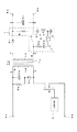
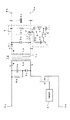
図1は、この発明によるスイッチングレギュレータの第1の実施の形態の構成を示す回路図である。この図1乃至図6までの各図において、前述した従来例の図8と対応する部分には同じ符号を付してあり、それらの詳細な説明は省略する。
この図1に示すスイッチングレギュレータは、他励ON−OFF方式の構成のDC−DCコンバータ2であり、フィルタ回路を除く回路構成は図8に示した従来のスイッチングレギュレータと同様である。
Hereinafter, the best mode for carrying out the present invention will be specifically described with reference to the drawings.
[First Embodiment]
FIG. 1 is a circuit diagram showing a configuration of a switching regulator according to a first embodiment of the present invention. 1 to 6, the same reference numerals are given to the portions corresponding to FIG. 8 of the conventional example described above, and detailed description thereof will be omitted.
The switching regulator shown in FIG. 1 is a DC-
そして、トランスT1の2次巻線Lsの一方の端子cに整流ダイオードDrを介して接続された第1の出力ライン1における平滑コンデンサCrとの接続点pよりトランスT1の2次巻線Ls側の部分と、電位が安定している導体によるフレームグランド5との間に、抵抗R1とコンデンサC1とインダクタ(コイル)L1を直列に接続した第1のフィルタ回路6を接続して設けている。
また、2次巻線Lsの他方の端子dに接続された第2の出力ライン2における平滑コンデンサCrとの接続点qよりトランスT1の2次巻線Ls側の部分とフレームグランド5との間に、抵抗R2とコンデンサC2とインダクタ(コイル等の誘導素子)L2を直列に接続した第2のフィルタ回路7を接続して設けている。
この実施形態では、電位が安定している導体によるフレームグランド5を、このスイッチングレギュレータの金属製の筐体としている。
Then, the secondary winding Ls side of the transformer T1 from the connection point p with the smoothing capacitor Cr in the
Also, between the
In this embodiment, the
すなわち、図1において破線で囲んで示す部分が電磁波ノイズを除去あるいは抑制するためのフィルタ回路部分である。なお、第1のフィルタ回路6と第2のフィルタ回路7の両方を設けた方がよいが、そのいずれか一方を設けるだけでもよい。
また、整流第ダオードDrは、2次巻線Ls一方の端子cにアノードを接続し、カソードに第1の出力ライン1を接続して正の直流電圧を出力するようにしているが、2次巻線Ls一方の端子cにカソードを接続し、アノードに第1の出力ライン1を接続して負の直流電圧を出力するようにしてもよい。
That is, a portion surrounded by a broken line in FIG. 1 is a filter circuit portion for removing or suppressing electromagnetic wave noise. In addition, although it is better to provide both the
The rectifying diode Dr is configured to output a positive DC voltage by connecting an anode to one terminal c of the secondary winding Ls and connecting the
このスイッチングレギュレータの動作について以下に説明する。
入力端子4a,4b間には、例えば商用電源の交流を全波整流回路で整流し、平滑回路によって平滑した直流が供給され、トランスT1の1次巻線Lpに電流を流す。その電流が、制御回路3によってスイッチング素子Qがオン/オフされることによって断続され、それによってトランスT1の2次巻線Lsに交流起電力が誘起される。
The operation of this switching regulator will be described below.
Between the
その交流電力を、整流ダイオードDrによって整流し、平滑コンデンサCrによって平滑して、出力端子8a,8b間に接続される負荷(使用機器)に直流電力を供給する。
そして、制御回路3がスイッチング素子Qをオン/オフ制御するパルスのデューティを増減することによって、スイッチング素子Qのオン時間を変化させ、出力電圧を制御することができる。
The AC power is rectified by the rectifier diode Dr, smoothed by the smoothing capacitor Cr, and the DC power is supplied to a load (use device) connected between the output terminals 8a and 8b.
Then, by increasing or decreasing the duty of the pulse for controlling the on / off of the switching element Q by the
この実施形態における第1,第2のフィルタ回路6、7は、以下に説明するように、このスイッチングレギュレータにおけるトランスT1の2次側において発生するノイズを効果的に低減することができる。
すなわち、スイッチングレギュレータの動作時には、上述したようにスイッチング素子Qのスイッチング制御によってトランスT1の1次巻線Lpに流れる電流が断続され、2次巻線Lsに交流電圧が誘起され、それが整流ダイオードDrによって整流された後に平滑コンデンサCrで平滑されることによって2次直流電力として出力される。
As described below, the first and
That is, during the operation of the switching regulator, as described above, the current flowing through the primary winding Lp of the transformer T1 is interrupted by the switching control of the switching element Q, and an AC voltage is induced in the secondary winding Ls, which is converted into a rectifier diode. After being rectified by Dr, smoothed by the smoothing capacitor Cr, it is output as secondary DC power.
そのスイッチング動作によってトランスT1の1次側でノイズが発生するとともに、2次側に生じるサージ電圧やリンギング状の電圧などが各素子を通過するときにもノイズが発生する。また、トランスT1の2次巻線Ls、整流ダイオードDr、第1の出力ライン1、平滑コンデンサCr及び第2の出力ライン2を結ぶ回路配線で電流ループが形成されることになる。
Due to the switching operation, noise is generated on the primary side of the transformer T1, and noise is also generated when a surge voltage or ringing voltage generated on the secondary side passes through each element. In addition, a current loop is formed by circuit wiring connecting the secondary winding Ls of the transformer T1, the rectifier diode Dr, the
この電流ループは、実際にはプリント配線基板の配線パターンで構成される場合が多いが、結合される各構成部品の大きさ、放熱性、電極間耐圧、安全規格などの回路構成の制約から、このループ面積をゼロにすることはできず、ある程度の長さを有するループ配線を形成することになる。そして、この電流ループの配線パターンにノイズ電流が流れた場合には、配線パターンの周囲に磁束が発生して電圧が誘起されることになり、この電流ループの配線パターンがループ状のアンテナを構成して周囲の空間に対し広くノイズを放射し、強い電磁障害を発生させる原因となる。 This current loop is actually often composed of a wiring pattern on a printed wiring board, but due to restrictions in circuit configuration such as the size of each component to be coupled, heat dissipation, withstand voltage between electrodes, and safety standards, This loop area cannot be made zero, and a loop wiring having a certain length is formed. When a noise current flows through the wiring pattern of this current loop, a magnetic flux is generated around the wiring pattern to induce a voltage, and this current loop wiring pattern constitutes a loop-shaped antenna. As a result, noise is widely radiated to the surrounding space, causing strong electromagnetic interference.
そこで、図8によって説明したように、この電流ループ(アンテナ)を構成する配線パターンとフレームグラウンド5との間にコンデンサだけを接続した場合、ある範囲の周波数帯域にあるノイズに対してはそのコンデンサがノイズだけを流すフィルタとして機能する。しかし、このコンデンサは、ある特定の周波数に対して、ループ配線がその長さと面積により潜在的に備えるインダクタンス成分と協働して共振状態となってしまい、しかもその共振が高いQを持っているため、ループ配線からノイズを強く放射してしまうことになる。
Therefore, as described with reference to FIG. 8, when only a capacitor is connected between the wiring pattern constituting the current loop (antenna) and the
これに対して、この実施形態における第1,第2のフィルタ回路6、7は、それぞれコンデンサC1、C2に直列に抵抗R1、R2を接続していることによって共振のQを下げて共振状態を弱め(Qダンプという)、放射エネルギを低減させるようにしている。つまり、共振回路のインダクタンス成分の値をL、容量成分の値をC、抵抗成分の値をRとすると、共振時のQは次式によって求められる。
Q=ωL/R=1/ωCR
したがって、抵抗R1、R2の抵抗値を大きくすることによって、Qを効果的にダンプさせることができる。
On the other hand, the first and
Q = ωL / R = 1 / ωCR
Therefore, Q can be effectively dumped by increasing the resistance values of the resistors R1 and R2.
また、共振状態でない場合でも、第1,第2のフィルタ回路6、7においてノイズ電流が抵抗R1、R2を通過する際には抵抗損失として発熱して消費されるとともに、抵抗R1、R2により電位差を持たせていることでノイズを落とされた先の電位(この実施形態では筐体の電位)が引き続き安定した電位を維持することができる。
Even when not in the resonance state, when the noise current passes through the resistors R1 and R2 in the first and
また、一般にコンデンサは使用可能な帯域に限界があり、第1,第2のフィルタ回路6、7のコンデンサC1、C2についても容量が大きければQをダンプさせる効果は大きいが、容量が大きいほど部品固有の共振状態で作用効果を発揮できる帯域が下がって、フィルタ効果がなくなってしまう。そのため、抵抗R1,R2によってQをダンプさせ、コンデンサC1、C2はあまり容量を大きくせずに有効な帯域を延ばし、装置の使用状態により共振点をシフトダウンもしくはシフトアップさせ、ノイズレベルを均一化させて電磁障害を低減させる。
In general, a capacitor has a limited usable bandwidth, and the capacitors C1 and C2 of the first and
また、第1フィルタ回路6は、整流ダイオードDrと第1の出力ライン1の平滑コンデンサCrとの接続点pとの間の部分とフレームグラウンド5との間に接続し、第2のフィルタ回路7は、トランスT1の2次巻線Lsの端子dと第2の出力ライン2の平滑コンデンサCrとの接続点qとの間の部分とフレームグラウンド5との間に接続しているので、ノイズが平滑コンデンサに達する手前で安定した電位に落すことができ、電流ループの面積を実質的に小さすることができる。
The
ここで、Kを定数、Sを電流ループの面積、Inをノイズ電流の大きさ、fをノイズ電流の周波数、dを導体厚さとした場合、電流ループの放射電解強度Eは、
E=K・S・In・f2/d
と表すことができる。したがって、上述のように電流ループの面積を小さくすることにより、電流ループから空間に放射される輻射ノイズを弱め、電磁障害を低減させることができる。
Here, when K is a constant, S is the area of the current loop, In is the magnitude of the noise current, f is the frequency of the noise current, and d is the conductor thickness, the radiative electrolytic strength E of the current loop is
E = K · S · In · f 2 / d
It can be expressed as. Therefore, by reducing the area of the current loop as described above, the radiation noise radiated from the current loop to the space can be weakened and electromagnetic interference can be reduced.
以上により、この発明によるスイッチングレギュレータ1は、高機能化、高出力化されたものであっても、2次側単独で広い帯域のノイズレベルを抑え、電流ループにおける共振状態および放射電解強度を弱めることができるため、効果的に電磁障害を低減させることができる。
なお、各フィルタ回路6、7における抵抗R1、R2とコンデンサC1、C2とインダクタL1、L2をそれぞれ直列に接続する順序は、図示の順に限るものではなく、任意の順序で接続すればよく、第1のフィルタ回路6と第2のフィルタ回路7でその接続順序が異なっていても構わない。また、第1フィルタ回路6又は第2フィルタ回路7の一方だけを設けてもよいことは前述したとおりであり、装置の使用状況によってはどちらか一方のみを設けるようにしてもよい。
As described above, the
Note that the order in which the resistors R1 and R2, the capacitors C1 and C2, and the inductors L1 and L2 are connected in series in the
スイッチングレギュレータで問題になる周波数は、スイッチング素子やダイオード等の部品の周波数特性や経験上から、スイッチング周波数(10KHz〜1MHz)から300MHz程度である。したがって、第1,第2フィルタ回路6,7のインダクタL1,L2の部品単体の自己共振点は、300MHz以上が好ましい。
しかし、特定のポイント、たとえば問題になる周波数が不要輻射の100MHzであれば、自己共振点が100MHzを越えるものであればよいし、雑音端子電圧の30MHzであれば、自己共振点が30MHzを越えるインダクタを選定すればよい。
The frequency which becomes a problem in the switching regulator is about 300 MHz to the switching frequency (10 KHz to 1 MHz) from the frequency characteristics and experience of components such as a switching element and a diode. Therefore, the self-resonance point of the single component of the inductors L1 and L2 of the first and
However, if a specific point, for example, the problematic frequency is 100 MHz of unwanted radiation, the self-resonance point may be higher than 100 MHz, and if the noise terminal voltage is 30 MHz, the self-resonance point exceeds 30 MHz. An inductor may be selected.
また、コンデンサC1,C2は、積層フィルムコンデンサ等の高周波対応のものを選定するのが望ましい。しかし、場合によっては貫通コンデンサでもよいし、単に空隙を介して対向する導電パターンによって形成してもよい。その場合の容量は、空隙の距離と対向する導電パターンの面積によって調整することができる。そして、空隙のために周波数の特性が伸び、広い帯域で使用できるコンデンサが得られる。このコンデンサの好ましい例に関しては、後述する図6に示すコンデンサC3に関しても同様である。
抵抗はR1,R2は、純粋な抵抗成分の抵抗値のみを示すものが望ましい。そのため、炭素被膜抵抗、酸化皮膜抵抗、金属被膜抵抗などの抵抗を使用する。巻線抵抗は、インタクタンス成分が大きいため使用しない方がよい。
Further, it is desirable to select capacitors C1 and C2 that are compatible with high frequencies such as laminated film capacitors. However, depending on the case, it may be a feedthrough capacitor or may be formed simply by conductive patterns facing each other through a gap. The capacity in that case can be adjusted by the area of the conductive pattern facing the gap distance. Further, the frequency characteristics are extended due to the gap, and a capacitor that can be used in a wide band is obtained. The same applies to a preferable example of this capacitor as to a capacitor C3 shown in FIG.
It is desirable that the resistances R1 and R2 indicate only the resistance values of pure resistance components. Therefore, resistances such as carbon film resistance, oxide film resistance, and metal film resistance are used. It is better not to use the winding resistance because the inductance component is large.
〔第2の実施の形態〕
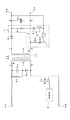
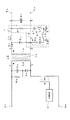
次に、この発明によるスイッチングレギュレータの第2の実施の形態について説明する。図2は、そのスイッチングレギュレータの構成を示す回路図である。
この実施形態において、図1に示した第1の実施形態と異なる点は、第1,第2のフィルタ回路6,7の共通接続端を接続する先を、第1の出力ラインにおける平滑コンデンサCrとの接続点pと出力端子8aとの間、すなわち平滑コンデンサCrによって平滑されて電位が安定した部分(配線パターンによる導体)とした点だけである。
このように、第1,第2のフィルタ回路6,7の一端の接続点であるもとの電流ループ上よりも電位の安定した配線パターン上に他端を接続しても、ノイズ電流をハイインピーダンスにせずに吸収させることができる。
[Second Embodiment]
Next, a second embodiment of the switching regulator according to the present invention will be described. FIG. 2 is a circuit diagram showing the configuration of the switching regulator.
In this embodiment, the difference from the first embodiment shown in FIG. 1 is that the common connection end of the first and
Thus, even if the other end is connected to a wiring pattern having a more stable potential than the original current loop, which is the connection point of one end of the first and
ここでいう電位の安定とは、必ずしも直流状態に近いという意味ではなく、交流状態においても安定していることをいい、インピーダンスについても同様である。各フィルタ回路6、7の両端をどのように接続するかによって生じる交流的な電位差が問題となる。もし、電流ループと各フィルタ回路6、7の接続先との間にあまり電位差がなく、抵抗損失を問題としない場合には、図示はしていないが、各フィルタ回路6、7にそれぞれ並列に抵抗を接続するようにしても有効である。そうすれば、各フィルタ回路6、7の両端間の電圧のインピーダンスを、それらの並列抵抗に強制的に押さえ込ませることになり、ノイズ低減のバランスを調整可能にする。
The stabilization of the potential here does not necessarily mean that it is close to the DC state, but it means that the potential is stable even in the AC state, and the same applies to the impedance. An AC potential difference caused by how to connect both ends of each
このようにして、スイッチングレギュレータが筐体を備えていないか(機器に内蔵される場合など)、樹脂等の絶縁材料製の筐体を使用する場合や、出力端子に接続される使用機器の状況によって基準電位(GND)が安定しない場合などでも、電流ループ上に発生したノイズ電流を他の電位の安定した配線パターンなどの導体へ落とすことによって、ループ面積を小さくでき、輻射ノイズの放射を低減することができる。 In this way, whether the switching regulator does not have a housing (such as when it is built into a device), when using a housing made of an insulating material such as resin, or the status of the device that is connected to the output terminal Even when the reference potential (GND) is not stable due to the noise, the loop area can be reduced by reducing the noise current generated on the current loop to a conductor such as a stable wiring pattern at other potentials, and radiation noise can be reduced. can do.
さらに、各フィルタ回路6、7の共通接続端を接続できる他の導体の例としては、フレーム、シャーシ、遮蔽板、ノイズ吸収体、他の部品の取り付け金具などの金属や、回路基板内の最も安定した電位を持つプリント配線パターン、例えば5Vの電位、3Vの電位の配線パターン等を使用することもできる。要は、ノイズ電流がハイインピーダンスにならずに吸収される電位の導体であればよい。
この場合も、第1のフィルタ回路6と第2のフィルタ回路7の一方のみを設けてもよいし、両方設ける場合にノイズ電流を落すために接続する先の導体が異なってもよい。
Furthermore, examples of other conductors that can connect the common connection ends of the
Also in this case, only one of the
〔第3の実施の形態〕
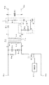
次に、この発明によるスイッチングレギュレータの第3の実施の形態について説明する。図3は、そのスイッチングレギュレータの構成を示す回路図である。
この実施形態において、図1に示した第1の実施形態と異なる点は、コンデンサC1と抵抗R1だけを直列に接続して構成した第1のフィルタ回路16と、コンデンサC2と抵抗R2だけを直列に接続して構成した第2のフィルタ回路17を、それぞれ第1のフィルタ回路6および第2のフィルタ回路7に代えて、第1の出力ライン1および第2の出力ライン2とフレームグランド5との間に接続して設けた点だけである。
[Third Embodiment]
Next explained is a third embodiment of the switching regulator according to the invention. FIG. 3 is a circuit diagram showing the configuration of the switching regulator.
This embodiment differs from the first embodiment shown in FIG. 1 in that a first filter circuit 16 configured by connecting only a capacitor C1 and a resistor R1 in series, and only a capacitor C2 and a resistor R2 are connected in series. In place of the
これは、負荷として接続される使用機器の状況や実際の回路構成によっては、共振点をシフトアップあるいはシフトダウンさせるためのインダクタを備える必要がなかったり、または限りなく小さいインダクタでよいために、各フィルタ回路16,17の配線自体に潜在的に有するインダクタンス成分で十分である場合があるためである。 Depending on the condition of the equipment used as a load and the actual circuit configuration, it may not be necessary to provide an inductor for shifting the resonance point up or down, or an infinitely small inductor may be used. This is because an inductance component potentially included in the wiring itself of the filter circuits 16 and 17 may be sufficient.
これは逆に、各フィルタ回路6、7が不要なインダクタを有したり、また余計なアンテナ源となることがないように回路の実装レイアウトを考慮する必要がある。また、抵抗R1、R2においてもインダクタンス成分を有する巻線抵抗などを用いないようにするのが望ましい理由でもある。
この場合も、第1,第2のフィルタ回路16,17のいずれか一方のみを設けてもよい。
また。図2に示した第2の実施形態における第1,第2のフィルタ回路6,7のインダクタL1,L2の両方あるいは一方を省略してもよい。
Conversely, it is necessary to consider the circuit layout so that the
Also in this case, only one of the first and second filter circuits 16 and 17 may be provided.
Also. Both or one of the inductors L1 and L2 of the first and
〔第4の実施の形態〕
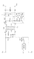
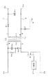
次に、この発明によるスイッチングレギュレータの第4の実施の形態について説明する。図4は、そのスイッチングレギュレータの構成を示す回路図である。
この実施形態で前述の第1実施形態と相違するのは、自励ON−OFF方式のDC−DCコンバータを構成するスイッチングレギュレータであり、それによる相違点のみを説明する。その他の、構成および作用・効果は図1に示した第1の実施形態と同じであるので、説明を省略する。
[Fourth Embodiment]
Next explained is the fourth embodiment of the switching regulator according to the invention. FIG. 4 is a circuit diagram showing the configuration of the switching regulator.
In this embodiment, what is different from the first embodiment described above is a switching regulator constituting a self-excited ON-OFF type DC-DC converter, and only the difference will be described. Other configurations, operations, and effects are the same as those of the first embodiment shown in FIG.
この実施形態で使用するトランスT2は、1次巻線Lpと2次巻線LsがコアTcに対して互いに同じ方向に巻かれている。そして、トランスT2の2次側の整流平滑回路4は、自励ON−OFF方式のDC−DCコンバータに対して力率を高くするためのチョークコイルLcと転流ダイオードDcとを設けている。チョークコイルLcは、第1出力ライン10上で整流ダイオードDrのカソードと第1フィルタ回路6と接続点eとの間に直列に接続して設けている。転流ダイオードDcは、第2出力ライン11上で2次巻線Lsの端子dと第2フィルタ回路7との接続点fとの間(図示の例では接続点fと同じ点になっている)にアノードを接続し、第1出力ライン10上で整流ダイオードDrのカソードとチョークコイルLcとの間にカソードを接続している。
In the transformer T2 used in this embodiment, the primary winding Lp and the secondary winding Ls are wound in the same direction with respect to the core Tc. The rectifying /
上述したようにトランスT2の1次巻線Lpと2次巻線LsがコアTcに対して互いに同じ方向に巻かれているため、トランジスタQのオン/オフによってトランスT2の1次巻線Lpに流れる電流が断続されると、2次巻線Lsに交流高電圧が誘起される。2次巻線Lsの端子cが正電位になったときに、2次電流が整流ダイオードDrを通してチョークコイルLcに流れて平滑コンデンサCrを充電するとともに、チョークコイルLcを励起する。 As described above, since the primary winding Lp and the secondary winding Ls of the transformer T2 are wound in the same direction with respect to the core Tc, the primary winding Lp of the transformer T2 is turned on / off by the transistor Q. When the flowing current is interrupted, an alternating high voltage is induced in the secondary winding Ls. When the terminal c of the secondary winding Ls becomes a positive potential, the secondary current flows to the choke coil Lc through the rectifier diode Dr, charges the smoothing capacitor Cr, and excites the choke coil Lc.
2次巻線Lsの端子cが0又は負電位になって整流ダイオードDrが非導通になったとき、チョークコイルLcに蓄積された励起エネルギが電流に再変換されて平滑コンデンサCrと転流ダイオードDcに流れ、平滑コンデンサCrを充電する。このようにしてトランスT2の2次巻線Lsに誘起された交流電力は整流・平滑され、出力端子8a、8bに直流電力が出力される。 When the terminal c of the secondary winding Ls becomes 0 or a negative potential and the rectifier diode Dr becomes non-conductive, the excitation energy accumulated in the choke coil Lc is reconverted into a current, and the smoothing capacitor Cr and the commutation diode. Flows through Dc and charges the smoothing capacitor Cr. The AC power induced in the secondary winding Ls of the transformer T2 in this way is rectified and smoothed, and DC power is output to the output terminals 8a and 8b.
この場合、第1のフィルタ回路6の第1の出力ライン1との接続点eは、平滑コンデンサCrとの接続点pとチョークコイルLcとの間にする。
この実施形態によっても、第1,第2のフィルタ6,7によるノイズ抑制あるいは低減作用は、前述した第1の実施形態の場合と同様である。
なお、第1実施形態と同様に第1,第2のフィルタ回路6、7はどちらか一方のみ設けてもよいし、抵抗R1、R2とコンデンサC1、C2とコイルL1、L2の接続順を任意に変えてもよい。また、コイルL1、L2の両方又は一方を省略してもよいし、ノイズを落とす接続先を筐体によるフレームグランド5に代えて、その他の電位の安定した配線パターンなどの導体としてもよい。
In this case, the connection point e of the
Also in this embodiment, the noise suppressing or reducing action by the first and
As in the first embodiment, only one of the first and
〔第5の実施の形態〕
次に、この発明によるスイッチングレギュレータの第5の実施の形態について説明する。図5は、そのスイッチングレギュレータの構成を示す回路図である。
この実施形態は、上述の第4実施例と殆ど同じであり、チョークコイルLcが第1の出力ライン1ではなく第2の出力ライン2に直列に、転流ダイオードとの接続点gと整流コンデンサCrとの接続点fとの間に設けた点が相違するだけである。
この実施形態によっても、図4に示した第4実施形態と同様な整流平滑作用が得られるとともに、各フィルタ回路6、7による電磁障害の低減作用も同様に得ることができる。
その種々の変更も、第4の実施形態において説明したのと同様に可能である。
[Fifth Embodiment]
Next explained is a fifth embodiment of the switching regulator according to the invention. FIG. 5 is a circuit diagram showing the configuration of the switching regulator.
This embodiment is almost the same as the fourth embodiment described above, and the choke coil Lc is connected in series with the
According to this embodiment, the same rectifying and smoothing action as that of the fourth embodiment shown in FIG. 4 can be obtained, and the electromagnetic interference reducing action by the
The various modifications are possible in the same manner as described in the fourth embodiment.
次に、この発明によるスイッチングレギュレータの第6の実施の形態について説明する。図6は、そのスイッチングレギュレータの構成を示す回路図である。
この実施形態も、前述した図4による第4の実施形態と殆ど共通しており、その相違点のみを説明する。
このスイッチングレギュレータは、第2フィルタ回路7の両端子間に並列に、そのコンデンサC2よりも容量の大きいコンデンサC3を接続して設けている点だけが第4の実施形態と相違している。これにより、第2フィルタ回路C3の両端間電圧が早く平滑されて各接続点が安定した電位になり、後述するように第2フィルタ回路7のノイズを低減させる効果が向上する。
Next, a sixth embodiment of the switching regulator according to the present invention will be described. FIG. 6 is a circuit diagram showing the configuration of the switching regulator.
This embodiment is almost in common with the above-described fourth embodiment shown in FIG. 4, and only the differences will be described.
This switching regulator is different from the fourth embodiment only in that a capacitor C3 having a larger capacity than that of the capacitor C2 is connected in parallel between both terminals of the
なお、図6ではこのような容量の大きいコンデンサを第2フィルタ回路7にしか接続していないが、第1フィルタ回路6の両端間にも、そのコンデンサC1よりも容量の大きいコンデンサを並列に接続して設けてもよい。また、前述した各実施形態と同様に種々の変更が可能である。
In FIG. 6, such a large-capacitance capacitor is connected only to the
〔この発明の実施例と従来例との比較説明〕
以下、この発明による実施例のスイッチングレギュレータと従来のスイッチングレギュレータのノイズ放射レベルについて比較して説明する。
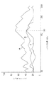
図7は、スイッチングレギュレータの作動時に発生す周波数に対するノイズの放射レベル(「ノイズレベル」と略称する)の計測値を示す線図であり、曲線Aは図8に示した従来例において発生するノイズレベル、曲線Bは図4に示したこの発明の第4の実施形態に基づく実施例において発生するノイズレベル、曲線Cは図6に示した第6の実施形態に基づく実施例おいて発生するノイズレベルを示している。
[Comparison between Example of the Invention and Conventional Example]
Hereinafter, the noise radiation levels of the switching regulator according to the embodiment of the present invention and the conventional switching regulator will be compared and described.
FIG. 7 is a diagram showing a measured value of a noise radiation level (abbreviated as “noise level”) with respect to a frequency generated when the switching regulator is operated, and a curve A is noise generated in the conventional example shown in FIG. Level and curve B are noise levels generated in the example based on the fourth embodiment of the present invention shown in FIG. 4, and curve C is noise generated in the example based on the sixth embodiment shown in FIG. Indicates the level.
なお、いずれの場合もスイッチングレギュレータの入力電源としては、100V、50Hzの商用交流電力を入力して、それを図示していない回路で整流・平滑した直流電力をトランスの1次側に供給し、スイッチング素子Qを130kHzのスイッチング周波数で駆動することによって、出力端子8a、8bから5V、20Aの直流電力を出力する設計となっている。 In any case, as an input power source of the switching regulator, 100V, 50 Hz commercial AC power is input, and DC power rectified and smoothed by a circuit (not shown) is supplied to the primary side of the transformer. By driving the switching element Q at a switching frequency of 130 kHz, it is designed to output DC power of 5V, 20A from the output terminals 8a, 8b.
この発明の第4,第6の実施形態に基づく実施例では、第1,第2のフィルタ回路6、7の各構成部品のパラメータとして、抵抗R1の抵抗値が10Ω、抵抗R2の抵抗値が4.7Ω、コンデンサC1、C2のキャパシタンスが1000pF、コイルL1、L2のインダクタンスが0.5μH(自己共振点は300MHz)、コンデンサC3のキャパシタンスが1μFとした。
In the examples based on the fourth and sixth embodiments of the present invention, the resistance value of the resistor R1 is 10Ω and the resistance value of the resistor R2 is a parameter of each component of the first and
従来のスイッチングレギュレータでは、図7に曲線Aで示されるように、コンデンサCの容量と電流ループのインダクタンス成分とによって、130MHz付近で共振状態となり、強い輻射ノイズを放射していることが判る。そして、30NHz〜300MHzの全周波数帯域でノイズレベルが大きくなっている。
これに対して、この発明の第4の実施形態の実施例では、曲線Bで示されているように、共振点における放射エネルギーが大きく抑えられており、かつ全周波数領域においてもノイズレベルが低減している。
In the conventional switching regulator, as indicated by a curve A in FIG. 7, it is found that resonance occurs near 130 MHz due to the capacitance of the capacitor C and the inductance component of the current loop, and strong radiation noise is emitted. And the noise level is large in the entire frequency band of 30 NHz to 300 MHz.
On the other hand, in the example of the fourth embodiment of the present invention, as shown by the curve B, the radiant energy at the resonance point is greatly suppressed, and the noise level is reduced in the entire frequency range. doing.
これは、第1,第2のフィルタ回路6、7を設け、その抵抗R1、R2により共振状態のQをダンプするとともに、電流ループから放射される電磁波ノイズのエネルギーを下げ、ノイズ電流が落された導体(この場合筐体)の電位が引き続き安定に維持されることによる。さらに、抵抗R1、R2等により電位差が生じることことによって、ノイズ電流を抵抗損失に替え、コンデンサC1,C2によって平滑し、インダクタL1,L2によって共振点をシフトさせて、帯域全体でノイズを低減させていることにもよる。
This is because the first and
また、この場合の各フィルタ回路6、7に設けられたコイルL1、L2のインダクタは、トランスT2の2次側における不連続な電流を連続にし、ノイズ電流のピークツーピークの波高値を低減させる役割も果たしている。
さらに、この発明による第2フィルタ回路7にコンデンサC3を並列接続して追加した第6の実施形態の実施例によれば、曲線Cで示されるように、帯域全体でノイズレベルをさらに低減できることが明らかである。これは、コンデンサC3として積層コンデンサ等の大容量(この例では1μF)のコンデンサを使用することにより、フィルタ回路の端子間電圧をいち早く平滑させることができ、さらにノイズ低減を図ることができるためである。
In addition, the inductors of the coils L1 and L2 provided in the
Furthermore, according to the example of the sixth embodiment in which the capacitor C3 is connected in parallel to the
この発明は、高機能化デジタル機器などの電子機器に対して安定した直流電力を供給するスイッチング電源に適用することができる。回路方式も自励式、他励式にかかわらず、またON−OFF方式だけでなくON−ON方式などの各種回路方式のものに適用できる。 The present invention can be applied to a switching power supply that supplies stable DC power to electronic devices such as highly functional digital devices. Regardless of whether the circuit system is self-excited or separately-excited, it can be applied to various circuit systems such as the ON-ON system as well as the ON-OFF system.
1:第1の出力ライン 2:第2の出力ライン 3:制御回路 4a,4b:入力力端子 5:フレームグラウンド 6,16:第1のフィルタ回路 7,17:第2のフィルタ回路 8a.8b:出力端子 T1:トランス Lp:1次巻線 Ls:2次巻線 Q:スイッチング素子 Dr:整流ダイオード Cr:平滑コンデンサ Lc:チョークコイル Dc:転流ダイオード C1,C2,C3:フィルタ回路のコンデンサ R1,R2:フィルタ回路の抵抗 L1,L2:フィルタ回路のインダクタ
1: first output line 2: second output line 3: control
Claims (4)
抵抗とコンデンサを直列に接続したフィルタ回路を、前記第1の出力ラインと前記第2の出力ラインのうちの少なくとも一方における前記平滑コンデンサとの接続点より前記トランスの2次巻線側の部分と、電位が安定している導体との間に接続して設けたことを特徴とするスイッチングレギュレータ。 A transformer that induces AC power in the secondary winding by interrupting a current flowing in the primary winding, a first output line connected to one terminal of the secondary winding via a rectifier diode, and In a switching regulator including a rectifying and smoothing circuit formed by connecting a smoothing capacitor between the second output line connected to the other terminal of the secondary winding,
A filter circuit in which a resistor and a capacitor are connected in series is connected to a portion on the secondary winding side of the transformer from a connection point of the smoothing capacitor in at least one of the first output line and the second output line. A switching regulator characterized by being connected between a conductor having a stable potential.
4. The switching regulator according to claim 1, wherein the conductor having a stable potential is a casing of the switching regulator. 5.
Priority Applications (1)
| Application Number | Priority Date | Filing Date | Title |
|---|---|---|---|
| JP2004107734A JP4473624B2 (en) | 2004-03-31 | 2004-03-31 | Switching regulator |
Applications Claiming Priority (1)
| Application Number | Priority Date | Filing Date | Title |
|---|---|---|---|
| JP2004107734A JP4473624B2 (en) | 2004-03-31 | 2004-03-31 | Switching regulator |
Publications (3)
| Publication Number | Publication Date |
|---|---|
| JP2005295700A true JP2005295700A (en) | 2005-10-20 |
| JP2005295700A5 JP2005295700A5 (en) | 2007-05-10 |
| JP4473624B2 JP4473624B2 (en) | 2010-06-02 |
Family
ID=35328023
Family Applications (1)
| Application Number | Title | Priority Date | Filing Date |
|---|---|---|---|
| JP2004107734A Expired - Fee Related JP4473624B2 (en) | 2004-03-31 | 2004-03-31 | Switching regulator |
Country Status (1)
| Country | Link |
|---|---|
| JP (1) | JP4473624B2 (en) |
Cited By (4)
| Publication number | Priority date | Publication date | Assignee | Title |
|---|---|---|---|---|
| AT13872U1 (en) * | 2013-05-02 | 2014-10-15 | Tridonic Gmbh & Co Kg | Operating device for bulbs |
| CN108336898A (en) * | 2018-04-11 | 2018-07-27 | 四川升华电源科技有限公司 | Brick filter module and power supply module |
| CN116567906A (en) * | 2023-06-26 | 2023-08-08 | 江苏神州半导体科技有限公司 | Ignition circuit structure of plasma system and ignition protection method |
| WO2025204820A1 (en) * | 2024-03-28 | 2025-10-02 | ミネベアミツミ株式会社 | Power supply device |
Families Citing this family (1)
| Publication number | Priority date | Publication date | Assignee | Title |
|---|---|---|---|---|
| CN102891486B (en) * | 2012-09-29 | 2015-04-15 | 沈阳鼎盛中贝机电设备有限公司 | Power grid filter circuit structure |
-
2004
- 2004-03-31 JP JP2004107734A patent/JP4473624B2/en not_active Expired - Fee Related
Cited By (6)
| Publication number | Priority date | Publication date | Assignee | Title |
|---|---|---|---|---|
| AT13872U1 (en) * | 2013-05-02 | 2014-10-15 | Tridonic Gmbh & Co Kg | Operating device for bulbs |
| US9532429B2 (en) | 2013-05-02 | 2016-12-27 | Tridonic Gmbh & Co Kg | Operating device for luminous elements |
| CN108336898A (en) * | 2018-04-11 | 2018-07-27 | 四川升华电源科技有限公司 | Brick filter module and power supply module |
| CN116567906A (en) * | 2023-06-26 | 2023-08-08 | 江苏神州半导体科技有限公司 | Ignition circuit structure of plasma system and ignition protection method |
| CN116567906B (en) * | 2023-06-26 | 2024-01-30 | 江苏神州半导体科技有限公司 | Ignition circuit structure of plasma system and ignition protection method |
| WO2025204820A1 (en) * | 2024-03-28 | 2025-10-02 | ミネベアミツミ株式会社 | Power supply device |
Also Published As
| Publication number | Publication date |
|---|---|
| JP4473624B2 (en) | 2010-06-02 |
Similar Documents
| Publication | Publication Date | Title |
|---|---|---|
| JP5375322B2 (en) | Charger | |
| US7978485B2 (en) | Thyristor power control circuit with damping circuit maintaining thyristor holding current | |
| AU2006242563B2 (en) | Electronic ballast having a flyback cat-ear power supply | |
| JPWO2014112639A1 (en) | Power transmission system | |
| CN106068679A (en) | Common-Mode Noise Suppression of Switch-Mode Power Converters via Capacitive Shields with Damping Networks | |
| JP2003051394A (en) | Discharge lamp lighting device | |
| JP2004023825A (en) | Power conversion circuit | |
| JP6758504B2 (en) | Welding current source | |
| JP4473624B2 (en) | Switching regulator | |
| CN103004069B (en) | Power source circuit | |
| JP3986462B2 (en) | High frequency heating device | |
| JP6120544B2 (en) | Lighting device and lighting apparatus | |
| CN104518692A (en) | A switching power supply that harvests radiated electromagnetic interference and harnesses its energy | |
| JP2011152019A (en) | Power supply apparatus | |
| JP2000341951A (en) | Switching power supply | |
| JP2011176981A (en) | Inverter circuit | |
| EP1410489B1 (en) | Power converters | |
| JP2006351353A (en) | Discharge lamp lighting device | |
| JP7614557B2 (en) | Power supply and lighting equipment | |
| JP6489042B2 (en) | Switching power supply device and noise filter | |
| JP2894145B2 (en) | Induction heating cooker | |
| JPH05130782A (en) | Discharge lamp operating device | |
| US20120112653A1 (en) | Electronic ballast for operating at least one discharge lamp | |
| JP2008078717A (en) | Noise filter and switching power source | |
| KR20040031503A (en) | Snuber circuit and Switching Mode Power Supply thereof |
Legal Events
| Date | Code | Title | Description |
|---|---|---|---|
| A521 | Written amendment |
Free format text: JAPANESE INTERMEDIATE CODE: A523 Effective date: 20070316 |
|
| A621 | Written request for application examination |
Free format text: JAPANESE INTERMEDIATE CODE: A621 Effective date: 20070316 |
|
| A977 | Report on retrieval |
Free format text: JAPANESE INTERMEDIATE CODE: A971007 Effective date: 20091022 |
|
| A131 | Notification of reasons for refusal |
Free format text: JAPANESE INTERMEDIATE CODE: A131 Effective date: 20091027 |
|
| A521 | Written amendment |
Free format text: JAPANESE INTERMEDIATE CODE: A523 Effective date: 20091225 |
|
| TRDD | Decision of grant or rejection written | ||
| A01 | Written decision to grant a patent or to grant a registration (utility model) |
Free format text: JAPANESE INTERMEDIATE CODE: A01 Effective date: 20100302 |
|
| A01 | Written decision to grant a patent or to grant a registration (utility model) |
Free format text: JAPANESE INTERMEDIATE CODE: A01 |
|
| A61 | First payment of annual fees (during grant procedure) |
Free format text: JAPANESE INTERMEDIATE CODE: A61 Effective date: 20100305 |
|
| FPAY | Renewal fee payment (event date is renewal date of database) |
Free format text: PAYMENT UNTIL: 20130312 Year of fee payment: 3 |
|
| R150 | Certificate of patent or registration of utility model |
Free format text: JAPANESE INTERMEDIATE CODE: R150 |
|
| FPAY | Renewal fee payment (event date is renewal date of database) |
Free format text: PAYMENT UNTIL: 20140312 Year of fee payment: 4 |
|
| R250 | Receipt of annual fees |
Free format text: JAPANESE INTERMEDIATE CODE: R250 |
|
| FPAY | Renewal fee payment (event date is renewal date of database) |
Free format text: PAYMENT UNTIL: 20140312 Year of fee payment: 4 |
|
| S111 | Request for change of ownership or part of ownership |
Free format text: JAPANESE INTERMEDIATE CODE: R313113 |
|
| R350 | Written notification of registration of transfer |
Free format text: JAPANESE INTERMEDIATE CODE: R350 |
|
| LAPS | Cancellation because of no payment of annual fees |