JP2005295553A - Method and means for isolating elements of a sensor array - Google Patents
Method and means for isolating elements of a sensor array Download PDFInfo
- Publication number
- JP2005295553A JP2005295553A JP2005097702A JP2005097702A JP2005295553A JP 2005295553 A JP2005295553 A JP 2005295553A JP 2005097702 A JP2005097702 A JP 2005097702A JP 2005097702 A JP2005097702 A JP 2005097702A JP 2005295553 A JP2005295553 A JP 2005295553A
- Authority
- JP
- Japan
- Prior art keywords
- substrate
- cmut
- elements
- acoustic
- transducer
- Prior art date
- Legal status (The legal status is an assumption and is not a legal conclusion. Google has not performed a legal analysis and makes no representation as to the accuracy of the status listed.)
- Granted
Links
Images

Classifications
-
- B—PERFORMING OPERATIONS; TRANSPORTING
- B08—CLEANING
- B08B—CLEANING IN GENERAL; PREVENTION OF FOULING IN GENERAL
- B08B5/00—Cleaning by methods involving the use of air flow or gas flow
- B08B5/02—Cleaning by the force of jets, e.g. blowing-out cavities
- B08B5/023—Cleaning travelling work
-
- B—PERFORMING OPERATIONS; TRANSPORTING
- B06—GENERATING OR TRANSMITTING MECHANICAL VIBRATIONS IN GENERAL
- B06B—METHODS OR APPARATUS FOR GENERATING OR TRANSMITTING MECHANICAL VIBRATIONS OF INFRASONIC, SONIC, OR ULTRASONIC FREQUENCY, e.g. FOR PERFORMING MECHANICAL WORK IN GENERAL
- B06B1/00—Methods or apparatus for generating mechanical vibrations of infrasonic, sonic, or ultrasonic frequency
- B06B1/02—Methods or apparatus for generating mechanical vibrations of infrasonic, sonic, or ultrasonic frequency making use of electrical energy
- B06B1/0292—Electrostatic transducers, e.g. electret-type
-
- B—PERFORMING OPERATIONS; TRANSPORTING
- B06—GENERATING OR TRANSMITTING MECHANICAL VIBRATIONS IN GENERAL
- B06B—METHODS OR APPARATUS FOR GENERATING OR TRANSMITTING MECHANICAL VIBRATIONS OF INFRASONIC, SONIC, OR ULTRASONIC FREQUENCY, e.g. FOR PERFORMING MECHANICAL WORK IN GENERAL
- B06B1/00—Methods or apparatus for generating mechanical vibrations of infrasonic, sonic, or ultrasonic frequency
- B06B1/02—Methods or apparatus for generating mechanical vibrations of infrasonic, sonic, or ultrasonic frequency making use of electrical energy
- B06B1/06—Methods or apparatus for generating mechanical vibrations of infrasonic, sonic, or ultrasonic frequency making use of electrical energy operating with piezoelectric effect or with electrostriction
- B06B1/0607—Methods or apparatus for generating mechanical vibrations of infrasonic, sonic, or ultrasonic frequency making use of electrical energy operating with piezoelectric effect or with electrostriction using multiple elements
- B06B1/0622—Methods or apparatus for generating mechanical vibrations of infrasonic, sonic, or ultrasonic frequency making use of electrical energy operating with piezoelectric effect or with electrostriction using multiple elements on one surface
- B06B1/0629—Square array
-
- F—MECHANICAL ENGINEERING; LIGHTING; HEATING; WEAPONS; BLASTING
- F24—HEATING; RANGES; VENTILATING
- F24F—AIR-CONDITIONING; AIR-HUMIDIFICATION; VENTILATION; USE OF AIR CURRENTS FOR SCREENING
- F24F3/00—Air-conditioning systems in which conditioned primary air is supplied from one or more central stations to distributing units in the rooms or spaces where it may receive secondary treatment; Apparatus specially designed for such systems
- F24F3/12—Air-conditioning systems in which conditioned primary air is supplied from one or more central stations to distributing units in the rooms or spaces where it may receive secondary treatment; Apparatus specially designed for such systems characterised by the treatment of the air otherwise than by heating and cooling
- F24F3/16—Air-conditioning systems in which conditioned primary air is supplied from one or more central stations to distributing units in the rooms or spaces where it may receive secondary treatment; Apparatus specially designed for such systems characterised by the treatment of the air otherwise than by heating and cooling by purification, e.g. by filtering; by sterilisation; by ozonisation
- F24F3/167—Clean rooms, i.e. enclosed spaces in which a uniform flow of filtered air is distributed
-
- G—PHYSICS
- G10—MUSICAL INSTRUMENTS; ACOUSTICS
- G10K—SOUND-PRODUCING DEVICES; METHODS OR DEVICES FOR PROTECTING AGAINST, OR FOR DAMPING, NOISE OR OTHER ACOUSTIC WAVES IN GENERAL; ACOUSTICS NOT OTHERWISE PROVIDED FOR
- G10K11/00—Methods or devices for transmitting, conducting or directing sound in general; Methods or devices for protecting against, or for damping, noise or other acoustic waves in general
- G10K11/002—Devices for damping, suppressing, obstructing or conducting sound in acoustic devices
Landscapes
- Engineering & Computer Science (AREA)
- Mechanical Engineering (AREA)
- Physics & Mathematics (AREA)
- Acoustics & Sound (AREA)
- Multimedia (AREA)
- Chemical & Material Sciences (AREA)
- Combustion & Propulsion (AREA)
- General Engineering & Computer Science (AREA)
- Ultra Sonic Daignosis Equipment (AREA)
- Transducers For Ultrasonic Waves (AREA)
- Investigating Or Analyzing Materials By The Use Of Ultrasonic Waves (AREA)
Abstract
【課題】 超微細加工超音波トランスデューサ(MUT)を提供する。
【解決手段】 装置は、半導体の表面を有する基板(4)上又は基板中に構築されたセンサ・アレイ(2、39、40)と、各センサ素子をその隣接する素子と絶縁する手段(26、28、30、32、34、36、38又は46)とを備える。センサが超音波トランスデューサ素子である場合、音響クロストークを低減するために隣接するトランスデューサ素子間のトレンチの形態で音響絶縁が形成される。トレンチは音響減衰材料で充填することができる。電気クロストークを低減するために、半導体接合形態の電気的絶縁が隣接するトランスデューサ素子間で形成される。1つの実施例において、隣接するトランスデューサ素子間に配置された区域にイオン注入することによりバックツーバックpn接合ダイオードが形成される。これらの形式の絶縁は、単独又は共に用いることができる。
【選択図】 図6An ultra-fine processed ultrasonic transducer (MUT) is provided.
The apparatus comprises a sensor array (2, 39, 40) constructed on or in a substrate (4) having a semiconductor surface, and means (26) for isolating each sensor element from its adjacent elements. , 28, 30, 32, 34, 36, 38 or 46). If the sensor is an ultrasonic transducer element, acoustic insulation is formed in the form of trenches between adjacent transducer elements to reduce acoustic crosstalk. The trench can be filled with an acoustic damping material. In order to reduce electrical crosstalk, electrical insulation in the form of semiconductor junctions is formed between adjacent transducer elements. In one embodiment, a back-to-back pn junction diode is formed by ion implantation in an area located between adjacent transducer elements. These types of insulation can be used alone or together.
[Selection] Figure 6
Description
本発明は、一般に、センサ・アレイ(例えば光、熱、圧力、超音波)に関する。具体的には、本発明は、超微細加工超音波トランスデューサ(MUT)に関する。MUTの1つの特定の応用は、医用診断超音波イメージング・システムにおいてである。別の特定の実施例は、キャスティング、鍛造、又はパイプラインなどの材料の非破壊評価(NDE)においてである。 The present invention relates generally to sensor arrays (eg, light, heat, pressure, ultrasound). Specifically, the present invention relates to a micromachined ultrasonic transducer (MUT). One particular application of MUT is in medical diagnostic ultrasound imaging systems. Another specific example is in non-destructive evaluation (NDE) of materials such as casting, forging, or pipelines.
通常の超音波イメージング・トランスデューサは、分極した圧電セラミック材料を用いて電気エネルギを音響エネルギに変換する、圧電効果により音響エネルギを発生する。スキャンされる患者の方向である前方方向へ送信される音響エネルギは、1つ又はそれ以上の音響マッチング層を通して患者に結合される。しかしながら、スキャンされる患者から離れる方向に送信される音響エネルギは通常、トランスデューサ・アレイの背面に配置される音響バッキング材料で吸収及び/又は散乱される。これにより、音響エネルギがトランスデューサの背面にある構造又はインターフェースから反射して圧電材料に戻ることにより、患者内の反射から得られる音響画像の品質が低下することを防ぐ。音響バッキング材料の多くの組成は公知である。例えば、音響バッキング材料は、ゴム、エポキシ、又はプラスチックなどの減衰軟質材料の金属粒子(例えばタングステン)の複合材からなるものとすることができる。また、他の音響バッキングの組成も用いてもよい。 Conventional ultrasound imaging transducers generate acoustic energy by the piezoelectric effect, using polarized piezoelectric ceramic material to convert electrical energy into acoustic energy. Acoustic energy transmitted in the forward direction, which is the direction of the patient being scanned, is coupled to the patient through one or more acoustic matching layers. However, acoustic energy transmitted away from the patient being scanned is typically absorbed and / or scattered by an acoustic backing material located on the back of the transducer array. This prevents acoustic energy from being reflected from the structure or interface on the back of the transducer and returning to the piezoelectric material, thereby reducing the quality of the acoustic image resulting from reflection within the patient. Many compositions of acoustic backing materials are known. For example, the acoustic backing material may consist of a composite of metal particles (eg, tungsten) of a damped soft material such as rubber, epoxy, or plastic. Other acoustic backing compositions may also be used.
医用診断イメージングに用いられる超音波トランスデューサは、広帯域幅を有し、低レベルの超音波信号に対して高感度であり、これらの特性により高画質の生成が可能である。この基準を満たし、超音波トランスデューサの製造に従来から用いられている圧電材料は、ジルコン酸チタン酸鉛(PZT)セラミック及びポリフッ化ビニリデン樹脂を含む。しかしながら、PZTトランスデューサは、半導体構成要素などの超音波システムの他の部品を製造するのに用いられるプロセス技術と異なるセラミック製造プロセスを必要とする。超音波トランスデューサは、半導体構成要素を製造するのに用いられるものと同じプロセスを用いて製造するのが望ましい。 Ultrasonic transducers used for medical diagnostic imaging have a wide bandwidth and are highly sensitive to low-level ultrasonic signals, and these characteristics enable generation of high image quality. Piezoelectric materials that meet this standard and are conventionally used in the manufacture of ultrasonic transducers include lead zirconate titanate (PZT) ceramics and polyvinylidene fluoride resins. However, PZT transducers require a ceramic manufacturing process that is different from the process technology used to manufacture other parts of the ultrasound system, such as semiconductor components. Ultrasonic transducers are preferably manufactured using the same process used to manufacture semiconductor components.
最近、半導体プロセスを用いて、容量型(cMUT)又は圧電型(pMUT)などとすることができる超微細加工超音波トランスデューサ(MUT)として公知の形式の超音波トランスデューサが製造されている。cMUTは、受信される超音波信号の音響振動を変調されたキャパシタンスに変換する電極を備えた、微小なダイヤフラム様装置である。送信については、容量電荷を変調して装置のダイヤフラムを振動させることにより、音波を送信する。pMUTは、ダイヤフラムが圧電型材料とシリコン窒化物又はシリコンなどの不活性材料とからなり、バイモルフであること以外は同様である。 Recently, a known type of ultrasonic transducer has been manufactured as a micromachined ultrasonic transducer (MUT) that can be capacitive (cMUT) or piezoelectric (pMUT), etc., using semiconductor processes. A cMUT is a micro diaphragm-like device with electrodes that convert the acoustic vibration of a received ultrasonic signal into a modulated capacitance. For transmission, sound waves are transmitted by modulating the capacitive charge and vibrating the device diaphragm. The pMUT is the same except that the diaphragm is composed of a piezoelectric material and an inert material such as silicon nitride or silicon and is a bimorph.
MUTの1つの利点は、これらが「微細加工」として分類される超微細製造プロセスなどの半導体製造プロセスを用いて製造できることである。超微細加工は、米国特許第6,359,367号において以下のように説明されている。
「微細加工とは、(A)パターン形成ツール(一般に投影アライナー又はウェーハステッパーなどのリソグラフィ)と、(B)PVD(物理的蒸着)、CVD(化学気相蒸着)、LPCVD(低圧化学気相蒸着)、PECVD(プラズマ化学気相蒸着)などの蒸着ツールと、(C)湿式化学エッチング、プラズマエッチング、イオンミリング、スパッターエッチング、又はレーザーエッチングなどのエッチングツールとの組合せ又はこれらの一部を使用した微細構造形成である。微細加工は通常、シリコン、ガラス、サファイア、又はセラミックから作られた基板又はウェーハ上で行なわれる。このような基板又はウェーハは、一般に極めて平坦且つ滑らかであり、横方向で数インチの大きさを有する。これらは通常、プロセスツール毎に移動しながらカセット中のグループとして処理される。各基板は有利には、製品の多数のコピーを(必ずしもそうとは限らないが)組み込むことができる。微細加工には2つの一般的なタイプがあり、すなわち、1)ウェーハ又は基板が形作られる厚みの大きな部分を有するバルク微細加工と、2)造形が一般に表面、特に表面上に堆積された薄いフィルムに限定される表面微細加工である。ここで使用される微細加工の定義には、シリコン、サファイア、全てのタイプのガラス材料、ポリマー(ポリイミド等)、ポリシリコン、シリコン窒化物、シリコン酸化窒化物、アルミニウム合金及び銅合金及びタングステンなどの薄膜金属、スピン・オン・ガラス(SOG)、埋め込み可能又は拡散型の添加物、並びにシリコン酸化物及び窒化物などの成長フィルムを含む、従来型の又は既知の微細加工できる材料の使用が含まれる。」
本明細書でも超微細加工の同様の定義を採用する。かかる超微細加工プロセスによって得られるシステムは、通常「超微細加工電気機械システム」(MEMS)と呼ばれる。
One advantage of MUTs is that they can be manufactured using semiconductor manufacturing processes such as ultra-fine manufacturing processes that are classified as “microfabrication”. Ultrafine processing is described in US Pat. No. 6,359,367 as follows.
“Microfabrication means (A) patterning tools (typically lithography such as projection aligners or wafer steppers), (B) PVD (physical vapor deposition), CVD (chemical vapor deposition), LPCVD (low pressure chemical vapor deposition) ), A combination of a deposition tool such as PECVD (plasma chemical vapor deposition) and (C) an etching tool such as wet chemical etching, plasma etching, ion milling, sputter etching, or laser etching, or a part thereof Microfabrication is usually performed on a substrate or wafer made of silicon, glass, sapphire, or ceramic, which is generally very flat and smooth and laterally Have a size of a few inches, these usually move with each process tool However, each substrate can advantageously incorporate (although not necessarily) multiple copies of the product.There are two general types of microfabrication. 1) bulk micromachining with a thick portion where the wafer or substrate is formed, and 2) surface micromachining where shaping is generally limited to the surface, in particular thin films deposited on the surface. The definition of microfabrication used includes silicon, sapphire, all types of glass materials, polymers (polyimide, etc.), polysilicon, silicon nitride, silicon oxynitride, aluminum alloys and copper alloys, and thin film metals such as tungsten , Spin-on-glass (SOG), embeddable or diffusive additives, and silicon oxides and nitrides Including growth film includes the use of conventional or known microfabrication can material. "
In this specification, the same definition of ultrafine processing is adopted. A system obtained by such a microfabrication process is usually referred to as a “micromachined electromechanical system” (MEMS).
容量型超微細加工超音波トランスデューサ装置を用いて発生される音響エネルギは、超音波エネルギを発生するのに圧電材料に依存しない。むしろ、cMUTセルの基本構造は、小ギャップにより導電性電極の上方に懸架された導電性膜又はダイヤフラムのものである。電圧が膜と電極の間に印加されると、クーロン力が膜を電極に引き付ける。印加電圧が経時的に変化すると、膜の位置も同様に変化し、膜が位置を移動するにつれて装置の表面から放射する音響エネルギが発生する。音響エネルギは主として前方、すなわち患者方向に発生するが、音響エネルギの一部はcMUT支持構造内に伝播される。この構造は一般的には、高濃度ドープのシリコーンウェーハ、すなわち半導体ウェーハである。 The acoustic energy generated using the capacitive micromachined ultrasonic transducer device does not depend on the piezoelectric material to generate ultrasonic energy. Rather, the basic structure of the cMUT cell is that of a conductive membrane or diaphragm suspended above the conductive electrode by a small gap. When a voltage is applied between the membrane and the electrode, Coulomb forces attract the membrane to the electrode. As the applied voltage changes over time, the position of the membrane changes as well, generating acoustic energy that radiates from the surface of the device as the membrane moves in position. While acoustic energy occurs primarily forward, i.e. in the direction of the patient, a portion of the acoustic energy is propagated into the cMUT support structure. This structure is typically a heavily doped silicone wafer, ie a semiconductor wafer.
cMUT装置は通常、トランスデューサ素子につき複数の膜で構築される。医用イメージング、非破壊評価、又は他のイメージング装置に用いられる完全なトランスデューサ・プローブは、アレイを形成するように1つ又は複数の横列に配列された複数のトランスデューサ素子を含み、各素子は共に電気的に接続された電極を有する複数のcMUTセルから構成される。アレイの各素子は、隣接する素子とは独立して動作する必要がある。トランスデューサ素子のアレイは共通の基板上に構築されるので、隣接する素子間に電気的及び機械的両方の障害(すなわちクロストーク)が存在することになるといった問題がある。
MUT(cMUT及びpMUT)装置のトランスデューサ素子間に絶縁を形成する必要性がある。 There is a need to form insulation between the transducer elements of MUT (cMUT and pMUT) devices.
本発明は、基板上又は基板内に構築されたセンサのアレイを含む装置、及び各センサ素子をその隣接する素子と絶縁する手段に関する。半導体ウェーハの場合、半導体表面は通常、半導体ウェーハの1つの面であるが、これはまた、絶縁基板上の半導体の薄膜であってもよい。本発明はまた、かかる装置を製造する方法に関する。開示された幾つかの実施形態によると、音響クロストークを低減する音響絶縁が隣接するセンサ素子間に形成される。開示された別の実施形態によると、電気的クロストークを低減する電気的絶縁が隣接するセンサ素子間に形成される。これらの形式の絶縁は、センサ装置に単独又は共に用いることができる。センサは、光、熱、又は圧力センサ、或いは超音波トランスデューサとすることができる。 The present invention relates to a device comprising an array of sensors built on or in a substrate and means for insulating each sensor element from its adjacent elements. In the case of a semiconductor wafer, the semiconductor surface is usually one side of the semiconductor wafer, but it may also be a semiconductor thin film on an insulating substrate. The invention also relates to a method of manufacturing such a device. According to some disclosed embodiments, acoustic isolation that reduces acoustic crosstalk is formed between adjacent sensor elements. According to another disclosed embodiment, electrical insulation that reduces electrical crosstalk is formed between adjacent sensor elements. These types of insulation can be used alone or together in the sensor device. The sensor can be a light, heat, or pressure sensor, or an ultrasonic transducer.
本発明の1つの態様は、基板の前面に配列され、各々が基板の材料と接触する複数のセンサ素子と、任意のセンサ素子間のエネルギ形態での結合を低減するように基板の材料内に配列され、各々がそこに入射するエネルギ形態の伝播に対する障害をもたらす複数の障壁とを備えるセンサ装置である。 One aspect of the present invention is a plurality of sensor elements arranged in front of the substrate, each in contact with the substrate material, and within the substrate material to reduce coupling in energy form between any sensor elements. A sensor device comprising a plurality of barriers arranged and each providing an obstacle to the propagation of energy forms incident thereon.
本発明の別の態様は、センサ装置の製造方法であり、(a)基板内又は基板上にセンサ素子のアレイを超微細加工する段階と、(b)任意のセンサ素子間のエネルギ形態での結合を低減するように、各々がそこに衝突するエネルギ形態の伝播に対する障害をもたらす複数の障壁を基板の材料内に形成する段階とを含む。 Another aspect of the present invention is a method for manufacturing a sensor device, comprising: (a) microfabricating an array of sensor elements in or on a substrate; and (b) in an energy form between any sensor elements. Forming a plurality of barriers in the substrate material that impede the propagation of energy forms that each impinge thereon so as to reduce coupling.
本発明の更に別の態様は、超音波トランスデューサ装置であり、基板の前面に配列され、その各々が電気的に共に接続され且つ基板に音響的に結合された超音波トランスデューサ・セルのそれぞれのグループを含む複数の超音波トランスデューサ素子と、トランスデューサ素子間の領域に配置され、そこを通る音波エネルギの伝播を妨げる、基板の材料内の複数のトレンチとを備える。 Yet another aspect of the present invention is an ultrasonic transducer device, each group of ultrasonic transducer cells arranged on the front surface of a substrate, each of which is electrically connected together and acoustically coupled to the substrate. And a plurality of trenches in the material of the substrate disposed in a region between the transducer elements and preventing propagation of sonic energy therethrough.
本発明の更に別の態様は、基板の前面に配列され、各々が基板の材料に接触する複数のセンサ素子と、センサ素子間の領域に配置され、そこを通る電流の流れを妨げる、基板の材料にドーパント注入する複数の帯域とを含むセンサ装置である。 Yet another aspect of the present invention provides a plurality of sensor elements arranged in front of the substrate, each disposed in a region between the sensor elements that contact the material of the substrate and preventing current flow therethrough. And a plurality of zones for injecting dopants into the material.
本発明の更に別の態様は、センサ装置の製造方法であり、(a)基板の一方の面にセンサ・アレイを超微細加工する段階と、(b)基板の一方の面又は他方の面を第1の支持構造体に取り付ける段階と、(c)支持構造体に取り付けられていない基板の面上の材料にセンサ素子間の領域に配置される複数のトレンチを形成する段階とを含む。 Yet another embodiment of the present invention is a method for manufacturing a sensor device, wherein (a) a sensor array is subjected to ultrafine processing on one surface of the substrate, and (b) one surface or the other surface of the substrate is formed. Attaching to the first support structure; and (c) forming a plurality of trenches disposed in a region between the sensor elements in a material on a surface of the substrate not attached to the support structure.
本発明の他の態様は以下に開示され請求される。 Other aspects of the invention are disclosed and claimed below.
ここで異なる図面の同じ要素に同じ参照番号が付与された図面を参照する。 Reference is now made to the drawings in which the same elements in different drawings have been given the same reference numerals.
説明のために、容量型超微細加工超音波トランスデューサ(cMUT)の部類に属する本発明の様々な実施形態を説明する。しかしながら、本明細書で開示される本発明の各態様は、cMUTの構造又は製造に限定されるものではなく、基板上の他のタイプのセンサ・アレイの構造又は製造にも適用されることは理解されたい。本発明は半導体材料で製造された基板にも限定されない。 For purposes of explanation, various embodiments of the invention belonging to the class of capacitive micromachined ultrasonic transducers (cMUTs) will be described. However, each aspect of the invention disclosed herein is not limited to cMUT structure or manufacture, but can be applied to the structure or manufacture of other types of sensor arrays on a substrate. I want you to understand. The present invention is not limited to substrates made of semiconductor materials.
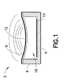
図1を参照すると、典型的なcMUTトランスデューサ・セル2の断面が示されている。このようなcMUTトランスデューサ・セルのアレイは、一般に、高濃度にドープされたシリコン(従って半導体性)ウェーハなどの基板4上に作製される。各cMUTトランスデューサ・セルでは、シリコン又はシリコン窒化物で作ることができる薄膜又はダイヤフラム8が基板4上に懸架される。膜8は、シリコン酸化物、シリコン窒化物、又は基板材料で製造することができる絶縁支持体6によってその周縁部で支持される。膜8と基板4との間のキャビティ16は、空気又は気体で充填してもよく、或いは完全に又は部分的に真空にすることができる。アルミニウム合金又は他の好適な導電性材料などの導電性材料のフィルム又は層は、膜8上に電極12を形成し、導電性材料で作られた別のフィルム又は層は、基板4上に電極10を形成する。或いはまた、底部電極は、基板の好適なドーピングで形成することができる。図1に示されるように、電極12は膜の最上部にあるが、膜の中に埋め込むか、又は膜の底面に置くこともできる。
Referring to FIG. 1, a cross section of a typical
2つの電極10及び12は、キャビティ16によって離隔されて、キャパシタンスを形成する。入射する音響信号が膜8を振動させると、関連する電子回路構成(図1には図示せず)を用いてキャパシタンスの変化を検出することができ、これにより音響信号を電気信号に変換することができる。反対に電極の1つに印加されたAC信号は電極上の電荷を変調して、電極間の容量力に変調を生じさせ、これがダイヤフラムを移動させることにより音響信号を送出する。
The two
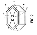
典型的なcMUTはミクロンサイズの寸法であるので、多数のcMUTセルが通常近接して製造されて、単一のトランスデューサ素子を形成する。個々のセルは、円形、矩形、六角形、又は他の周囲形状を有することができる。最密を達成する単純な形状のうち、六角形が最も円形に近く、従って最も単純な共鳴モードを有する。六角形であるcMUTセルが図2に示されている。六角形は、トランスデューサ素子のcMUTセルの高密実装をもたらす。cMUTセルは、トランスデューサ素子が異なるセル・サイズの複合的特性を有し、トランスデューサに対してより広帯域特性を与えるように、異なる寸法を有することができる。セルを互いに電気的に接続する図2に示される「スポーク」14は、図1のアイテム12で参照されるパターン化された電極の部品である。電極12は最適な音響性能のためにパターン化することができ、膜8の底部に配置することができる。
Since typical cMUTs are micron-sized, a number of cMUT cells are usually manufactured in close proximity to form a single transducer element. Individual cells can have a circular, rectangular, hexagonal, or other surrounding shape. Of the simple shapes that achieve close packing, the hexagon is closest to the circle and thus has the simplest resonance mode. A cMUT cell that is hexagonal is shown in FIG. The hexagon provides a high density packaging of the cMUT cell of the transducer element. cMUT cells can have different dimensions so that the transducer elements have a composite characteristic of different cell sizes, giving the transducer more broadband characteristics. The “spokes” 14 shown in FIG. 2 that electrically connect the cells to each other are part of the patterned electrode referenced in
cMUT装置は更に、本明細書で「音響バッキング」と呼ばれる音響減衰材料の層を含み、これは、基板の背面に音響的に結合される。音響バッキング層は、極めて薄い基板の構造的支持をもたらすのに十分な剛性を有する。かかる音響バッキング層は、例えばほぼ音響的に透明であるのに十分に薄いエポキシ層を用いて基板の背面に直接接合することができ、或いは介在層を用いて基板に積層することができる。或いはまた、音響バッキングは、十分な音響インピーダンを有するキャスト又は成型可能な組成物とすることができる。1つの実施形態において、介在層は、シリコン基板の音響インピーダンスと音響減衰材料の音響インピーダンスとの間の音響インピーダンスを有する音響インピーダンス・マッチング材料で製造される。別の実施形態において、介在層は、基板内で導電性バイアに接続する導電性パッドを有する可撓性プリント回路基板(「フレックス回路」)である。音響バッキングは、基板内の横方向に伝播する波が、トランスデューサ素子間のクロストークが低減する程度まで吸収されるような減衰性能を有するのが好ましい。 The cMUT device further includes a layer of sound attenuating material, referred to herein as an “acoustic backing”, which is acoustically coupled to the back surface of the substrate. The acoustic backing layer is sufficiently rigid to provide structural support for a very thin substrate. Such an acoustic backing layer can be bonded directly to the back of the substrate, for example using an epoxy layer that is thin enough to be substantially acoustically transparent, or can be laminated to the substrate using an intervening layer. Alternatively, the acoustic backing can be a cast or moldable composition with sufficient acoustic impedance. In one embodiment, the intervening layer is made of an acoustic impedance matching material having an acoustic impedance between the acoustic impedance of the silicon substrate and the acoustic impedance of the acoustic damping material. In another embodiment, the intervening layer is a flexible printed circuit board (“flex circuit”) having conductive pads that connect to conductive vias in the substrate. The acoustic backing preferably has an attenuation capability so that waves propagating laterally within the substrate are absorbed to the extent that crosstalk between transducer elements is reduced.
図3は、好適な電子回路構成(図示せず)に電気的接続(例えばフレックス回路)22及び24を介して接続されたcMUT装置20の側面図を示す。(本明細書で用いられる用語「cMUT装置」は、基板と該基板により支持される複数のcMUTセルを含む構造を意味する。)図示された実施形態において、cMUT装置20は、音響バッキング材料18の本体に形成されるウェルに載置される。基板の最上部は、基板の占有面積を越えて延びる音響バッキングの部分の最上部とほぼ同じ高さに位置し、可撓性電気的接続22及び24の遠位端は基板の各端部と重なり、可撓性電気的接続22及び24の隣接部分は音響バッキング層のそれぞれの部分と重なり接合される。図3に見られるように、音響バッキング層18は、cMUT装置20並びに可撓性電気的接続22及び24を支持する。音響バッキング18は、cMUT装置20に直接積層することができ、或いは前述のように、音響インピーダンス・マッチング介在層を積層スタックに含めることもできる。
FIG. 3 shows a side view of a
超微細加工された超音波トランスデューサ・アレイは、基板の表面上に構築することができ、又は基板から材料を除去することで蝕刻することができる。アレイは、1つ又は複数の行のトランスデューサ素子を含むことができ、又はトランスデューサ素子は、米国特許出願番号第10/383,990号に開示されるような、cMUTセル又は素子が基板上にモザイク模様にされた、いわゆる「モザイク・アレイ」などの横列を持たない2次元配列で編成することができる。 The microfabricated ultrasonic transducer array can be built on the surface of the substrate or etched by removing material from the substrate. The array can include one or more rows of transducer elements, or transducer elements such as disclosed in US patent application Ser. No. 10 / 383,990, where cMUT cells or elements are mosaicked on a substrate. It can be organized in a two-dimensional array with no rows, such as a so-called “mosaic array” that is patterned.
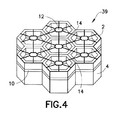
典型的なcMUT装置の各トランスデューサ素子は、複数のcMUTセルで構築される。説明のために、図4は7つの六角形cMUTセル2から作られた「デイジー」トランスデューサ素子を示し、これは中央のセルが6つのセルのリングで囲まれ、リングの各セルが中央のセルのそれぞれの辺とリングの隣接するセルと接している。各セル2の上部電極12は、互いに電気的に接続されている(この接続は切替可能に切断することができない)。六角形アレイの場合、6つの導体14(図2及び図4の両方に示す)は上部電極12から外側に放射状に広がり、それぞれが隣接し合うcMUTセルの上部電極に接続される(6つでなく、3つの他のセルに接続される周辺セルの場合を除く)。同様に、各セル2の底部電極10は互いに電気的に接続され、7倍の大きな容量型トランスデューサ素子39を形成する。
Each transducer element of a typical cMUT device is constructed with multiple cMUT cells. For illustration purposes, FIG. 4 shows a “daisy” transducer element made from seven
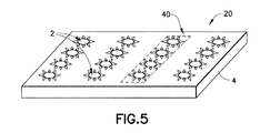
図4に見られるセルの配列は、1つの方向に延びて、全体的には矩形の長いトランスデューサ素子40を形成することができる。これらの矩形のトランスデューサ素子は、1つの横列に配列して、線形アレイを形成することができる。かかるcMUT装置20は、全体的に図5に示され、各矩形トランスデューサ素子40は、図面の簡略化のため単一の縦列のcMUTセルを有するように描かれているが、実際には各素子は、複数の縦列のcMUTセルを含むことを理解されたい。
The array of cells seen in FIG. 4 can extend in one direction to form a generally rectangular
アレイの各トランスデューサ素子は、その隣接する素子から独立して動作する必要がある。図5に示すように、アレイは共通の基板4上に構築されるので、隣接する素子間で電気的及び機械的な両方の障害(すなわちクロストーク)が存在する可能性があるという問題がある。本発明は素子間に必要とされる絶縁を形成する。
Each transducer element in the array must operate independently of its neighboring elements. As shown in FIG. 5, since the array is built on a
本発明の第1の部類の実施形態によると、隣接するトランスデューサ素子間の基板材料の全て又は一部を除去することによって絶縁が形成される。これは、ウェーハ・ダイシングソー、レーザ、ウェットエッチング法、反応性イオンエッチング(RIE)、又は深いRIEを用いて達成することができる。 According to a first class of embodiments of the present invention, the insulation is formed by removing all or part of the substrate material between adjacent transducer elements. This can be accomplished using a wafer dicing saw, laser, wet etching, reactive ion etching (RIE), or deep RIE.
絶縁トレンチを生成する1つの方法は、図3に見られるように、cMUTセル又は素子を支持する基板をバッキング材料に最初に取り付けることである。図6は、音響減衰材料から作られたバッキング層18に積層された基板4を示す。ウェーハ・ダイシングソー(図示せず)を用いて、基板4を切り通し、バッキング材料18を分けることにより、図6に見られる絶縁トレンチ26のような複数の離隔した、互いに平行な絶縁トレンチ又はチャネルを形成する。cMUT装置の動作周波数に応じて、基板4を完全に切断する必要がない場合もある。その代わりに、同様に図6に示されるように、基板4の全厚みよりも浅い深さの絶縁トレンチ又はチャネル28を形成することができる。簡潔にするために、深さの異なるトレンチが同じ図面内に示されていること、及び特定のcMUTウェーハの絶縁トレンチは通常同じ深さであることを理解されたい。
One way to create an isolation trench is to first attach a substrate supporting a cMUT cell or device to the backing material, as seen in FIG. FIG. 6 shows the
絶縁トレンチが基板4の全体の厚みを貫通してバッキング層18の中へ通る場合において、バッキング材料は各トランスデューサ素子に機械的支持をもたらすことになる。バッキング材料は、音響エネルギを減衰させるので、バッキング層18を通るクロストークは基板4を通るクロストークよりもかなり少なくなる。
In the case where the insulating trench passes through the entire thickness of the
絶縁トレンチの深さに関係なく、該絶縁トレンチは、隣接するトランスデューサ素子間に空間を置いて配置される。図6は、1つの横列のトランスデューサ素子を示し、各トランスデューサ素子は複数のcMUTセル2を含む。1つの横列の素子を有する線形アレイの場合には、互いに平行な絶縁トレンチは、隣接する素子間で空間を置いて配置される。アレイが2つ又はそれ以上の横列を含む場合には、絶縁トレンチはまた、横列間で空間を置いて配置され、各横列内でトレンチを交差させて、絶縁トレンチの相互接続ネットワークを形成する。この場合、横列間の絶縁トレンチは、互いに平行で、各横列内にある絶縁トレンチに対しては垂直である。各横列の内の素子が整列して縦列を形成する場合には、交差する絶縁トレンチは格子又はグリッドを形成することになる。
Regardless of the depth of the isolation trench, the isolation trench is placed with a space between adjacent transducer elements. FIG. 6 shows one row of transducer elements, each transducer element including a plurality of
トランスデューサ素子が音響的に絶縁されると、トランスデューサ素子間の絶縁トレンチは、シリコーンゴムなどの吸音材料で充填することができる。レンズがcMUT装置の表面に接着される場合には、音波の集束及び/又は装置の表面の保護のいずれかのために、レンズ接着剤を用いた絶縁トレンチの充填によりcMUT装置へのレンズの接着が改善される。素子間のトレンチの充填はまた、素子への機械的支持を付加する。 Once the transducer elements are acoustically isolated, the isolation trench between the transducer elements can be filled with a sound absorbing material such as silicone rubber. If the lens is glued to the surface of the cMUT device, the lens is bonded to the cMUT device by filling the insulating trench with a lens adhesive for either focusing of sound waves and / or protecting the surface of the device. Is improved. Filling the trenches between the elements also adds mechanical support to the elements.
トレンチの構造が最適形状を有するべきであることも決定することができる。図7を参照すると、絶縁トレンチは、直角の底部のプロファイル(トレンチ30参照)を有する必要はなく、代わりに、プロファイルは「V」(トレンチ32参照)又は「U」(図示せず)形の形状とすることができる。図6のトレンチ34及び36は、他のプロファイルを示している。トレンチ34のプロファイルは、平行な側壁とほぼ放物線形の底部プロファイルを有し、トレンチ36は平行な側壁とV型の底部プロファイルを有する。基板4に形成される絶縁トレンチの全ては通常、同じ形状のプロファイルを有しており、図6に示される異なる形状は、必要な図面数を最小限にするために1つの基板内に集められていることを理解されたい。
It can also be determined that the structure of the trench should have an optimal shape. Referring to FIG. 7, the isolation trench need not have a right bottom profile (see trench 30); instead, the profile is “V” (see trench 32) or “U” (not shown). It can be a shape. The
ダイシングソーの使用は、結果として得られる切り口つまりトレンチが直線的な幾何形状である限り、トランスデューサ素子間に配置される基板材料を除去する効果的な方法である。材料が、直線でない線に沿って除去される必要がある場合には、レーザカット、ウェットエッチング法、又はRIEなどの他の方法がより適切である。この実施例は、円形(例えば環状アレイ)に構築された装置であろう。この円形トランスデューサ・アレイは、同心環状リングを形成し、従って円形の絶縁パターンを必要とする素子を有する。この幾何形状は、音響エネルギの点集束を可能にする。 The use of a dicing saw is an effective way to remove the substrate material that is placed between the transducer elements as long as the resulting cut or trench has a linear geometry. If the material needs to be removed along a non-straight line, other methods such as laser cutting, wet etching, or RIE are more appropriate. An example of this would be a device constructed in a circle (eg, an annular array). This circular transducer array has elements that form concentric annular rings and thus require a circular insulating pattern. This geometry allows point focusing of acoustic energy.
基板の片側上で上述の音響絶縁法のいずれかを実行することは、本発明の範囲内である。図8に示されるcMUTセルの反対側である装置の背面から材料が除去されると、絶縁トレンチ38が基板4の全厚みを通って延びていない限り、より大きな活性領域を得ることができる。この場合、トレンチは、cMUTセル又は素子の真下の領域を占有するよう形成することができる。
It is within the scope of the present invention to perform any of the acoustic isolation methods described above on one side of the substrate. When material is removed from the back side of the device opposite the cMUT cell shown in FIG. 8, a larger active area can be obtained as long as the
cMUT装置は、背面絶縁を形成するために前面(すなわちcMUTセル側)で支持される必要がある。しかしながら、cMUT装置は簡単に損傷する可能性があるので、ダイシング・テープは用いることができない。懸架された膜に貼り付けられたテープは引き剥がすことができる。本発明の1つの実施形態によれば、背面に音響絶縁を形成する間は、cMUT装置は、脆弱なcMUT膜と接触した状態で装置の前面に塗布された低温取付ワックスによって支持される。絶縁加工が完了し、ダイシング作業により発生した破片をcMUT装置から取り除くと、cMUTは、取付ワックスを除去する前に支持体が必要となる。この支持体は、前述の音響減衰バッキング材料とすることができる。cMUT装置が支持体に取り付けられると、取付ワックスを加熱して融解される。取付ワックスに対して好適な溶剤を用いて、cMUT装置からワックスを取り除くことになる。別の支持方法は、cMUTを活性領域の外側で支持して、直接膜に接着することを避けることだけである。 The cMUT device needs to be supported on the front side (i.e. cMUT cell side) to form backside insulation. However, dicing tape cannot be used because cMUT devices can be easily damaged. The tape attached to the suspended membrane can be peeled off. According to one embodiment of the present invention, the cMUT device is supported by a cold mounting wax applied to the front of the device in contact with the fragile cMUT membrane, while forming acoustic insulation on the back. When the insulation process is complete and debris generated by the dicing operation is removed from the cMUT device, the cMUT requires a support before removing the mounting wax. This support can be the acoustic damping backing material described above. When the cMUT device is attached to the support, the attachment wax is heated to melt. A suitable solvent for the mounting wax will be used to remove the wax from the cMUT device. Another support method is simply to support the cMUT outside the active area and avoid sticking it directly to the membrane.
cMUT素子の絶縁を形成する上述の方法のいずれかでは、微小亀裂などの損傷の可能性があり、これは活性cMUTセル中に広がる可能性がある。これにより、わずかに導電性液体が浸透して信号及び接地電極を短絡させることがある。本発明の別の態様は、スパッタ又は蒸着シリカ、シリコン窒化物、アルミナ、又は他の絶縁無機物などのコンフォーマルコーティングを施すことによる予防措置を提供し、このような欠陥を覆ってシールする。蒸着被膜加工は、卓越した整合性と厚さの均一性があるピンホールの無い被膜を形成することが可能であり、真空下で実行される。 Any of the above-described methods of forming the insulation of the cMUT element can cause damage such as microcracks, which can spread into the active cMUT cell. This can cause slight penetration of the conductive liquid and short circuit the signal and ground electrodes. Another aspect of the present invention provides precautions by applying a conformal coating such as sputtered or vapor deposited silica, silicon nitride, alumina, or other insulating minerals to seal over such defects. Vapor deposition processing can form pinhole-free coatings with excellent consistency and thickness uniformity and is performed under vacuum.
被膜プロセスは以下のようにして実行される。cMUT素子間から材料を除去して絶縁トレンチを形成した後、cMUTセルを清浄化して、そこに残されたどのような残留物も除去する。次にcMUT装置を真空中で高温で乾燥させる。cMUT装置は、乾燥後、スパッタ又は蒸気被膜機械中に置かれ、数ミクロンの選択された材料が被膜される。かかる被膜が極めてコンフォーマルであるとしても、十分に小さい場合には微小亀裂はシールされ、cMUTセルは真空になる。多くの絶縁無機物材料は、高い絶縁耐力を有し、これはcMUTセルを外部環境から絶縁するのに役立つ。 The coating process is performed as follows. After removing material from between the cMUT elements to form an isolation trench, the cMUT cell is cleaned to remove any residue left there. The cMUT device is then dried at high temperature in a vacuum. After drying, the cMUT device is placed in a sputter or vapor coating machine and coated with a selected material of a few microns. Even if such a coating is very conformal, if it is small enough, the microcracks are sealed and the cMUT cell is evacuated. Many insulating inorganic materials have a high dielectric strength, which helps insulate the cMUT cell from the outside environment.
本発明の更に別の態様は、トランスデューサ素子が互いに電気的に絶縁されるcMUT装置の製造である。本発明の1つの実施形態によると、電気的絶縁は、選択的イオン注入により達成することができる。電気的結合は電磁エネルギの流れ、主に電子の流れによって支配されるので、該結合は基板の導電性を変更することで最小化することができる。より正確には、トランスデューサ素子間にある基板の特定の領域は、基板の半導体特性を変化させるイオンをドープすることができる。素子間の領域に選択的にドーパントを注入することで、バックツーバックpn接合ダイオードなどの接合、すなわち電気的クロストークを抑制する絶縁に近い領域を形成することができる。こ手法により、材料は除去されないが、電気特性が選択された領域において変更される。このプロセスは、cMUTセルの形成の前、途中、又は後で実行することができる。イオン注入条件が、cMUTセルの超微細加工中に支配的となる温度よりも高温を指示する場合には、超微細加工の前にイオン注入の実行を選択することができる。 Yet another aspect of the present invention is the manufacture of a cMUT device in which the transducer elements are electrically isolated from each other. According to one embodiment of the present invention, electrical isolation can be achieved by selective ion implantation. Since electrical coupling is dominated by the flow of electromagnetic energy, primarily the flow of electrons, the coupling can be minimized by changing the conductivity of the substrate. More precisely, certain regions of the substrate between the transducer elements can be doped with ions that change the semiconductor properties of the substrate. By selectively injecting the dopant into the region between the elements, a junction such as a back-to-back pn junction diode, that is, a region close to insulation that suppresses electrical crosstalk can be formed. This technique does not remove the material but changes the electrical properties in the selected region. This process can be performed before, during, or after the formation of the cMUT cell. If the ion implantation conditions indicate a higher temperature than the temperature that prevails during ultrafine processing of the cMUT cell, execution of ion implantation can be selected prior to ultrafine processing.
或いはまた、cMUT製造向けに主として非導電性基板を用いることができ、ここでは底部電極は、cMUTの下で堆積された金属又は選択的にドープされた領域のいずれかである。この場合、これらの領域を選択的にドープしてこれらを電気的に接地することにより、各素子間の領域を接地することが望ましい場合がある。(前述のように)絶縁トレンチにより離隔された素子間の領域を接地する別の方法は、トレンチの表面(例えば壁)をアルミニウム又はアルミニウム・シリコン合金などの導電性材料で被膜し、次いでこの金属を接地して隣接する素子間を電気的に絶縁することである。いずれかの方法により、浮遊電荷を隣接する素子ではなく接地に伝導することが可能となる。 Alternatively, a primarily non-conductive substrate can be used for cMUT fabrication, where the bottom electrode is either a metal deposited under the cMUT or a selectively doped region. In this case, it may be desirable to ground the regions between the elements by selectively doping these regions and electrically grounding them. Another method for grounding the region between the elements separated by the isolation trench (as described above) is to coat the surface (eg, wall) of the trench with a conductive material such as aluminum or aluminum-silicon alloy, and then this metal. Is grounded to electrically insulate adjacent elements. Either method allows floating charges to be conducted to ground instead of adjacent devices.
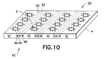
pn接合ダイオードは、面に沿って隣接するドープ半導体材料の2つのボリュームを含み、その面が接合を構成する。1つの区域の材料は、n型半導体材料であり、他方の区域の材料はp型材料である。すなわち半導体材料は、接合の片側で異なるようにドープされる。pn接合ダイオードは、一方向で導通し、他の方向では導通しない。2つのpn接合ダイオードをバックツーバックで配置することで、装置はどちらの方向にも導通しないように形成することができる。かかる1対のバックツーバックpn接合ダイオードの長さを延ばすことにより、電流の流れに対する長い障壁を形成することができる。図9及び図10は、かかる電気的絶縁デバイスの2つの実施例を示し、ここで基板4がドープされて、npn型のバックツーバックダイオードを形成する。いずれの場合においても、バックツーバックダイオードは、基板材料の要求された深さまでドープ剤を注入することにより作製される。
A pn junction diode includes two volumes of doped semiconductor material that are adjacent along a plane, which plane constitutes the junction. The material in one area is an n-type semiconductor material and the material in the other area is a p-type material. That is, the semiconductor material is doped differently on one side of the junction. A pn junction diode conducts in one direction and does not conduct in the other direction. By placing two pn junction diodes back-to-back, the device can be made to not conduct in either direction. By extending the length of such a pair of back-to-back pn junction diodes, a long barrier to current flow can be formed. FIGS. 9 and 10 show two examples of such an electrical isolation device, where the
図9に示される実施形態において、トランスデューサ素子(各素子が複数のcMUTセル2を含む)は、n型半導体材料で製造された各領域44及び48上に構築され、pドーパントはトランスデューサ素子間の領域46にイオン注入される。n型半導体材料で製造された各領域は、その上に構築されるトランスデューサ素子の底部電極として機能する。各p型領域は、それぞれのn型領域が両側面に位置してそれぞれのnp接合50及び52を形成する。或いはまた、トランスデューサ素子は、p型材料上に構築することができ、該p型領域はトランスデューサ素子間のイオン注入n型領域にインターリーブされる。
In the embodiment shown in FIG. 9, transducer elements (each element includes a plurality of cMUT cells 2) are built on each
図10に示される実施形態において、トランスデューサ素子は、p型でもn型でもない半導体すなわち非導電性(非ドープのポリシリコンなど)の材料で製造されたそれぞれ領域上に構築されると共に、隣接するトランスデューサ素子間に配置される各領域において、nドーパントは領域44及び48にイオン注入され、pドーパントは領域44と48との間の領域46にイオン注入される。この場合も、各p型領域は、それぞれのn型領域が両側面に位置してそれぞれのnp接合50及び52を形成する。或いはまた、npn接合の代わりに、pnp接合をトランスデューサ素子間の領域に注入することができる。
In the embodiment shown in FIG. 10, the transducer elements are built on and adjacent to each region made of a non-p-type or n-type semiconductor, i.e., non-conductive (such as undoped polysilicon) material. In each region located between the transducer elements, n dopant is ion implanted into
従って、隣接するトランスデューサ素子は、隣接するトランスデューサ素子間の非占有空間に図9又は図10で示されたタイプの障壁を配置することにより、互いに電気的に絶縁することができる。 Accordingly, adjacent transducer elements can be electrically isolated from each other by placing a barrier of the type shown in FIG. 9 or 10 in the unoccupied space between adjacent transducer elements.
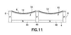
図11は、本発明の別の実施形態によるp型材料で製造された共通壁46を共有する2つのトランスデューサ素子の断面図を示す。簡潔にするために、追加のトランスデューサ素子は示されていないが、隣接するトランスデューサ素子の各ペアは、p型材料で製造された共通壁を共有することを理解されたい。それぞれの素子の底部電極は、n型材料のそれぞれの領域44及び46から成る。n型材料の隣接する領域間の領域はp型材料が占有し、このp型材料が上方に突出して共通壁を形成する。p型材料の壁は膜8を支持し、この膜はトランスデューサ素子を形成する個別のcMUTセルのそれぞれのキャビティ10の上に懸架される。特定のトランスデューサ素子のcMUTセルは、n型材料で製造された共通の底部電極を共有するのが好ましい。
FIG. 11 shows a cross-sectional view of two transducer elements sharing a
音響バッキング層が基板の背面に配置される実施形態において、音響バッキング材料は、cMUT基板に音響的に適合した組成を有するべきであり、音響エネルギの反射が装置に戻るのを防ぐ。基板4がシリコン製である場合、好適なバッキング材料の1つの実施例は、名称が「Backing Material for Micromachined Ultrasonic Transducer Devices」の米国特許出願番号第10/248,022号で開示されているように、(質量で)96.3%のタングステン(その85%は10ミクロンで15%は1ミクロンの粒径)と、3.67%のポリ塩化ビニル(PVC)粉体との混合物から構成される。タングステン―ビニル複合体はまた、Lees、Gilmore及びKranzによる研究論文「Acoustic Properties of Tungsten−Vinyl Composites」、IEEE Transactions on Sonics and Ultrasonics、SU−20巻、1号、pp.1−2、1月、1972年で検討されている。音響バッキング材料の組成は、上記で与えられた実施例から変更することができることは当業者には理解されるであろう。
In embodiments where the acoustic backing layer is disposed on the backside of the substrate, the acoustic backing material should have a composition that is acoustically compatible with the cMUT substrate, preventing reflection of acoustic energy from returning to the device. If the
更に、図3に示される実施形態は、cMUTアレイの上部に可撓性相互接続回路を配置することを含む。アレイを相互接続する別の可能な手段は、バッキング材料に埋め込まれるワイヤ又はトレースを介してバッキング材料を通る接続を形成することである。これらの接続は次に、ウェーハ貫通バイア又はラップアラウンド接続によってcMUT装置の表面上に形成することができる。別の変化形態により、フレックス回路を基板の下に配置することができ、次にウェーハ貫通バイア又はラップアラウンド接続を用いて、cMUT装置の上部に信号を送ることができる。別の変化形態により、cMUT基板を、インピーダンス・マッチング、多重化、スイッチング、及びビーム形成の送受信などの超音波変換から分離又は関連付けられた電気的機能を提供する第2の基板に接続することができる。音響バッキング層はこれらの基板の間に配置することができる。この実施形態において、cMUTセル電極から第2の基板の電子回路構成への電気的接続は、基板及び音響バッキング層で形成されるバイアを通過することができる。 In addition, the embodiment shown in FIG. 3 includes placing flexible interconnect circuitry on top of the cMUT array. Another possible means of interconnecting the array is to form a connection through the backing material via wires or traces embedded in the backing material. These connections can then be formed on the surface of the cMUT device by through-wafer vias or wrap-around connections. According to another variation, the flex circuit can be placed under the substrate and then a signal can be sent to the top of the cMUT device using a through-wafer via or wrap-around connection. According to another variation, the cMUT substrate may be connected to a second substrate that provides an electrical function that is separated or associated with ultrasonic transformations such as impedance matching, multiplexing, switching, and beamforming transmission and reception. it can. An acoustic backing layer can be disposed between these substrates. In this embodiment, the electrical connection from the cMUT cell electrode to the electronic circuit configuration of the second substrate can pass through a via formed by the substrate and the acoustic backing layer.
本発明を好ましい実施形態を参照して説明してきたが、本発明の範囲から逸脱することなく様々な変更を行うことができ、均等物をその要素と置き換えることができることは当業者には理解されるであろう。更に、本発明の本質的範囲から逸脱することなく特定の状況を本発明の教示に対して適合させるように多くの修正を行うことができる。従って本発明は、本発明を実行するにあたって考えられる最良のモードとして開示された特定の実施形態に限定されず、本発明は添付の請求項の範囲内に包含される全ての実施形態を含むことが意図される。 While the invention has been described with reference to preferred embodiments, those skilled in the art will recognize that various modifications can be made and equivalents can be substituted for the elements without departing from the scope of the invention. It will be. In addition, many modifications may be made to adapt a particular situation to the teachings of the invention without departing from the essential scope thereof. Accordingly, the invention is not limited to the specific embodiments disclosed as the best mode contemplated for carrying out the invention, and the invention includes all embodiments encompassed within the scope of the appended claims. Is intended.
請求項で用いられる用語「超音波トランスデューサ」は、容量型及び圧電型の超音波トランスデューサを含む。請求項で用いられる語句「基板を超微細加工する」は、表面及び/又はバルク双方の超微細加工を含むように解釈すべきである。また、図面の符号に対応する特許請求の範囲中の符号は、単に本願発明の理解をより容易にするために用いられているものであり、本願発明の範囲を狭める意図で用いられたものではない。そして、本願の特許請求の範囲に記載した事項は、明細書に組み込まれ、明細書の記載事項の一部となる。 The term “ultrasonic transducer” as used in the claims includes capacitive and piezoelectric ultrasonic transducers. The phrase “micromachining a substrate” as used in the claims should be interpreted to include both surface and / or bulk micromachining. Further, the reference numerals in the claims corresponding to the reference numerals in the drawings are merely used for easier understanding of the present invention, and are not intended to narrow the scope of the present invention. Absent. The matters described in the claims of the present application are incorporated into the specification and become a part of the description items of the specification.
2 cMUTトランスデューサ・セル
4 基板
18 バッキング層
26、28 絶縁トレンチ
2
Claims (10)
任意の前記センサ素子間のエネルギ形態での結合を低減するように前記基板の材料内に配列され、各々がそこに入射する前記エネルギ形態の伝播に対する障害をもたらす複数の障壁(26、28、30、32、34、36、38又は46)と、
を備えるセンサ装置。 A plurality of sensor elements (2, 39, 40) arranged on the front surface of the substrate, each contacting the material of the substrate;
A plurality of barriers (26, 28, 30) arranged in the material of the substrate to reduce coupling in the energy form between any of the sensor elements, each impeding the propagation of the energy form incident thereon. 32, 34, 36, 38 or 46), and
A sensor device comprising:
前記トランスデューサ素子間の領域に配置され、そこを通る音波エネルギの伝播を妨げる、前記基板の材料内の複数のトレンチ(26、28、30、32、34、36又は38)と、
を備える超音波トランスデューサ装置。 A plurality of ultrasonic transducer elements (2, 39, 40) arranged in front of a substrate (4), each of which is electrically connected together and acoustically coupled to said substrate The transducer element comprising a respective group of cells;
A plurality of trenches (26, 28, 30, 32, 34, 36 or 38) in the material of the substrate disposed in a region between the transducer elements and preventing propagation of sonic energy therethrough;
An ultrasonic transducer device comprising:
Applications Claiming Priority (2)
| Application Number | Priority Date | Filing Date | Title |
|---|---|---|---|
| US10/814,956 US20040190377A1 (en) | 2003-03-06 | 2004-03-31 | Method and means for isolating elements of a sensor array |
| US10/814,956 | 2004-03-31 |
Publications (2)
| Publication Number | Publication Date |
|---|---|
| JP2005295553A true JP2005295553A (en) | 2005-10-20 |
| JP4868758B2 JP4868758B2 (en) | 2012-02-01 |
Family
ID=35034299
Family Applications (1)
| Application Number | Title | Priority Date | Filing Date |
|---|---|---|---|
| JP2005097702A Expired - Fee Related JP4868758B2 (en) | 2004-03-31 | 2005-03-30 | Method and means for isolating elements of a sensor array |
Country Status (5)
| Country | Link |
|---|---|
| US (1) | US20040190377A1 (en) |
| JP (1) | JP4868758B2 (en) |
| KR (1) | KR20060044973A (en) |
| CN (1) | CN1677706A (en) |
| DE (1) | DE102005014836A1 (en) |
Cited By (18)
| Publication number | Priority date | Publication date | Assignee | Title |
|---|---|---|---|---|
| JP2007201753A (en) * | 2006-01-26 | 2007-08-09 | Hitachi Ltd | Ultrasonic probe |
| JP2007301023A (en) * | 2006-05-09 | 2007-11-22 | Hitachi Medical Corp | Ultrasonic probe |
| WO2008038454A1 (en) * | 2006-09-28 | 2008-04-03 | Hitachi, Ltd. | Ultrasonic probe and ultrasonic imaging device |
| JP2008148720A (en) * | 2006-12-14 | 2008-07-03 | Hitachi Medical Corp | Ultrasonic probe and ultrasonic diagnostic apparatus |
| WO2008114582A1 (en) * | 2007-03-20 | 2008-09-25 | Hitachi Medical Corporation | Ultrasonic probe and method for manufacturing the same and ultrasonic diagnostic device |
| JP2009207882A (en) * | 2008-02-08 | 2009-09-17 | Toshiba Corp | Ultrasonic probe and ultrasonic diagnosis apparatus |
| JP2010030034A (en) * | 2008-06-24 | 2010-02-12 | Canon Inc | Mechanoelectrical transduction element and manufacturing method of mechanoelectrical transduction apparatus |
| JP2010035156A (en) * | 2008-06-24 | 2010-02-12 | Canon Inc | Mechanoelectrical transducer and manufacturing method of same |
| WO2011105269A1 (en) * | 2010-02-26 | 2011-09-01 | 株式会社 日立メディコ | Ultrasonic probe and ultrasonic image pickup device using same |
| JP2013009233A (en) * | 2011-06-27 | 2013-01-10 | Ingen Msl:Kk | Vibration element, and manufacturing method of vibration element |
| JP5282305B2 (en) * | 2007-05-10 | 2013-09-04 | コニカミノルタ株式会社 | Ultrasonic probe and ultrasonic diagnostic apparatus |
| JP2015187576A (en) * | 2014-03-27 | 2015-10-29 | 国立研究開発法人日本原子力研究開発機構 | ultrasonic inspection apparatus |
| JP2017528032A (en) * | 2014-07-16 | 2017-09-21 | コーニンクレッカ フィリップス エヌ ヴェKoninklijke Philips N.V. | Tiled CMUT die with pitch uniformity |
| US11346953B2 (en) | 2018-07-20 | 2022-05-31 | Kabushiki Kaisha Toshiba | Photo detector, photo detection system, lidar device and vehicle |
| JP2022532834A (en) * | 2020-03-05 | 2022-07-20 | エクソ イメージング,インコーポレイテッド | Ultrasound imaging device with programmable anatomy and flow imaging |
| US11598858B2 (en) | 2019-08-29 | 2023-03-07 | Kabushiki Kaisha Toshiba | Light detector, light detection system, lidar device, and vehicle |
| JP2024513615A (en) * | 2021-03-29 | 2024-03-27 | エコー イメージング,インク. | Grooves to reduce crosstalk in MUT arrays |
| US12486159B2 (en) | 2021-06-30 | 2025-12-02 | Exo Imaging, Inc. | Micro-machined ultrasound transducers with insulation layer and methods of manufacture |
Families Citing this family (66)
| Publication number | Priority date | Publication date | Assignee | Title |
|---|---|---|---|---|
| US8576474B2 (en) | 2004-08-14 | 2013-11-05 | Fusao Ishii | MEMS devices with an etch stop layer |
| CN101558552B (en) * | 2005-06-17 | 2017-05-31 | 科隆科技公司 | Micro-electro-mechanical transducer with insulation extension |
| US7514851B2 (en) * | 2005-07-13 | 2009-04-07 | Siemens Medical Solutions Usa, Inc. | Curved capacitive membrane ultrasound transducer array |
| EP1950997B1 (en) * | 2005-10-18 | 2019-10-09 | Hitachi, Ltd. | Ultrasonic probe |
| JP4804961B2 (en) * | 2006-03-03 | 2011-11-02 | オリンパスメディカルシステムズ株式会社 | Ultrasonic transducer and intracorporeal ultrasonic diagnostic apparatus equipped with the same |
| JP4271252B2 (en) * | 2006-10-12 | 2009-06-03 | オリンパスメディカルシステムズ株式会社 | Ultrasonic transducer cell, ultrasonic transducer element, ultrasonic transducer array, and ultrasonic diagnostic apparatus |
| JP5009301B2 (en) * | 2006-11-08 | 2012-08-22 | 株式会社日立メディコ | Ultrasonic probe and ultrasonic diagnostic apparatus using the same |
| US20080242979A1 (en) * | 2007-03-30 | 2008-10-02 | Rayette Ann Fisher | Combined X-ray detector and ultrasound imager |
| JP5723775B2 (en) * | 2008-09-18 | 2015-05-27 | ビジュアルソニックス インコーポレイテッド | Ultrasonic transducer and other component manufacturing method |
| US9173047B2 (en) | 2008-09-18 | 2015-10-27 | Fujifilm Sonosite, Inc. | Methods for manufacturing ultrasound transducers and other components |
| US9184369B2 (en) | 2008-09-18 | 2015-11-10 | Fujifilm Sonosite, Inc. | Methods for manufacturing ultrasound transducers and other components |
| JP5409251B2 (en) * | 2008-11-19 | 2014-02-05 | キヤノン株式会社 | Electromechanical transducer and method for manufacturing the same |
| US20100168582A1 (en) * | 2008-12-29 | 2010-07-01 | Boston Scientific Scimed, Inc. | High frequency transducers and methods of making the transducers |
| US10129656B2 (en) * | 2009-01-30 | 2018-11-13 | Avago Technologies International Sales Pte. Limited | Active temperature control of piezoelectric membrane-based micro-electromechanical devices |
| JP5342005B2 (en) * | 2009-09-17 | 2013-11-13 | 株式会社日立メディコ | Ultrasonic probe and ultrasonic imaging apparatus |
| CN101719368B (en) * | 2009-11-04 | 2011-12-07 | 中国科学院声学研究所 | Device for directionally emitting sound wave with high sound intensity |
| JP2011259371A (en) * | 2010-06-11 | 2011-12-22 | Canon Inc | Manufacturing method of capacitive electromechanical transducer |
| JP4917699B2 (en) | 2010-08-06 | 2012-04-18 | オリンパスメディカルシステムズ株式会社 | Ultrasonic diagnostic equipment |
| US8409102B2 (en) | 2010-08-31 | 2013-04-02 | General Electric Company | Multi-focus ultrasound system and method |
| US20130331705A1 (en) * | 2011-03-22 | 2013-12-12 | Koninklijke Philips Electronics N.V. | Ultrasonic cmut with suppressed acoustic coupling to the substrate |
| US9530955B2 (en) | 2011-11-18 | 2016-12-27 | Acist Medical Systems, Inc. | Ultrasound transducer and processing methods thereof |
| CN102420286A (en) * | 2011-12-09 | 2012-04-18 | 中国船舶重工集团公司第七一五研究所 | Piezoelectric component having multilayer composite structure and preparation method thereof |
| US8541853B1 (en) * | 2012-03-22 | 2013-09-24 | Texas Instruments Incorporated | High frequency CMUT |
| US9454954B2 (en) | 2012-05-01 | 2016-09-27 | Fujifilm Dimatix, Inc. | Ultra wide bandwidth transducer with dual electrode |
| US8767512B2 (en) | 2012-05-01 | 2014-07-01 | Fujifilm Dimatix, Inc. | Multi-frequency ultra wide bandwidth transducer |
| US9061320B2 (en) * | 2012-05-01 | 2015-06-23 | Fujifilm Dimatix, Inc. | Ultra wide bandwidth piezoelectric transducer arrays |
| KR20140033992A (en) * | 2012-09-11 | 2014-03-19 | 삼성전자주식회사 | Ultrasonic transducer |
| KR101909131B1 (en) | 2012-09-11 | 2018-12-18 | 삼성전자주식회사 | Ultrasonic transducer and method of manufacturig the same |
| US9660170B2 (en) | 2012-10-26 | 2017-05-23 | Fujifilm Dimatix, Inc. | Micromachined ultrasonic transducer arrays with multiple harmonic modes |
| DE102012220811A1 (en) * | 2012-11-14 | 2014-05-15 | Intelligendt Systems & Services Gmbh | Device and method for ultrasonic testing of a component with an inclusions or cavities intermediate layer |
| EP2774389B1 (en) * | 2012-11-16 | 2018-04-11 | Acist Medical Systems, Inc. | Ultrasound transducer and manufacturing methods thereof |
| US20140184023A1 (en) * | 2012-12-31 | 2014-07-03 | Volcano Corporation | Layout and Method of Singulating Miniature Ultrasonic Transducers |
| KR101484959B1 (en) * | 2013-02-05 | 2015-01-21 | 삼성메디슨 주식회사 | Acoustic Transducer, Acoustic probe and Acoustic diagnostic equipment including the same |
| JP6273743B2 (en) * | 2013-09-30 | 2018-02-07 | セイコーエプソン株式会社 | Ultrasonic device and probe, electronic apparatus and ultrasonic imaging apparatus |
| KR102126033B1 (en) * | 2013-10-23 | 2020-06-23 | 삼성전자주식회사 | Ultrasonic transducer and ultrasonic diagnostic equipment including the same |
| US9536511B2 (en) | 2013-12-31 | 2017-01-03 | Acist Medical Systems, Inc. | Ultrasound transducer stack |
| US10182738B2 (en) | 2014-01-28 | 2019-01-22 | Vayyar Imaging Ltd | Sensors for a portable device |
| CN106660072B (en) * | 2014-07-16 | 2019-03-19 | 皇家飞利浦有限公司 | Tiled CMUT slices with pitch uniformity |
| JP6299511B2 (en) * | 2014-07-31 | 2018-03-28 | セイコーエプソン株式会社 | Ultrasonic device and probe and electronic equipment |
| KR20160023154A (en) * | 2014-08-21 | 2016-03-03 | 삼성전자주식회사 | untrasonic transducer |
| US10545107B2 (en) | 2015-04-26 | 2020-01-28 | Vayyar Imaging Ltd | System, device and methods for measuring substances' dielectric properties using microwave sensors |
| WO2016174679A2 (en) | 2015-04-27 | 2016-11-03 | Vayyar Imaging Ltd | System and methods for calibrating an antenna array using targets |
| WO2016174680A1 (en) | 2015-04-29 | 2016-11-03 | Vayyar Imaging Ltd | System, device and methods for localization and orientation of a radio frequency antenna array |
| US10690760B2 (en) | 2015-05-05 | 2020-06-23 | Vayyar Imaging Ltd | System and methods for three dimensional modeling of an object using a radio frequency device |
| US10809372B2 (en) | 2015-05-11 | 2020-10-20 | Vayyar Imaging Ltd. | System, device and methods for imaging of objects using electromagnetic array |
| EP3316792B1 (en) * | 2015-06-30 | 2019-05-22 | Koninklijke Philips N.V. | Intravascular ultrasound device with impedance matching structure |
| US10290948B2 (en) | 2015-08-02 | 2019-05-14 | Vayyar Imaging Ltd | System and method for radio frequency penetration imaging of an object |
| CN107920797B (en) * | 2015-09-03 | 2021-02-12 | 富士胶片索诺声公司 | Ultrasonic transducer assembly |
| US11084062B2 (en) | 2015-11-02 | 2021-08-10 | Koninklijke Philips N.V. | Ultrasound transducer array, probe and system |
| US10436896B2 (en) | 2015-11-29 | 2019-10-08 | Vayyar Imaging Ltd. | System, device and method for imaging of objects using signal clustering |
| JP2018019024A (en) * | 2016-07-29 | 2018-02-01 | キヤノン株式会社 | Printed board where vibration component for generating vibration |
| US10571415B2 (en) | 2016-08-02 | 2020-02-25 | Rolls-Royce Corporation | Methods and apparatuses for evaluating ceramic matrix composite components |
| FR3060844B1 (en) | 2016-12-15 | 2018-12-14 | Commissariat A L'energie Atomique Et Aux Energies Alternatives | ACOUSTIC MICROELECTRONIC DEVICE |
| EP3606094B1 (en) * | 2017-03-29 | 2025-04-02 | AGC Inc. | Glass plate component |
| CN107315070A (en) * | 2017-07-05 | 2017-11-03 | 南京航空航天大学 | A kind of structure of ultrasonic wave added type MOS gas sensors |
| CN108178121B (en) * | 2018-02-07 | 2024-05-03 | 北京先通康桥医药科技有限公司 | Palpation probe and manufacturing method thereof |
| EP3857308A4 (en) * | 2018-09-25 | 2022-06-08 | Exo Imaging Inc. | IMAGING DEVICES WITH SELECTIVELY MODIFIABLE CHARACTERISTICS |
| CN110448331B (en) * | 2019-09-12 | 2024-08-23 | 深圳市索诺瑞科技有限公司 | Air-filled ultrasonic transducer |
| US12372496B2 (en) | 2020-04-24 | 2025-07-29 | Agco Corporation | Methods of measuring harvested crop material |
| EP4139669B1 (en) | 2020-04-24 | 2025-01-15 | Agco Corporation | Agricultural machines comprising capacitive sensors, and related methods and apparatus |
| CN111884647B (en) * | 2020-08-13 | 2023-09-29 | 中国工程物理研究院电子工程研究所 | Coupling isolation method for piezoelectric micromechanical acoustic transducer array |
| CN113162460B (en) * | 2021-04-16 | 2023-05-30 | 西北工业大学 | Electrostatic rotary and linear reciprocating motion coupling energy collector |
| CN116553469A (en) * | 2022-03-24 | 2023-08-08 | 台湾积体电路制造股份有限公司 | Hybrid ultrasound transducer system |
| CN114890372B (en) * | 2022-05-07 | 2023-07-18 | 四川大学 | Design and preparation method of PMUT with isolation trench |
| EP4559588A1 (en) * | 2023-11-21 | 2025-05-28 | Dyconex AG | Ultrasound transducing device |
| CN118204255A (en) * | 2024-05-06 | 2024-06-18 | 西安交通大学 | A MEMS ultrasonic transducer array that realizes acoustic wave focusing guidance and edge vibration stopping functions by means of acoustic metamaterials and a preparation method thereof |
Citations (3)
| Publication number | Priority date | Publication date | Assignee | Title |
|---|---|---|---|---|
| JP2002209299A (en) * | 2000-12-28 | 2002-07-26 | Toshiba Corp | Semiconductor vibration sensor |
| WO2003011748A2 (en) * | 2001-07-31 | 2003-02-13 | Koninklijke Philips Electronics N.V. | Micro-machined ultrasonic transducer (mut) substrate that limits the lateral propagation of acoustic energy |
| JP2003520466A (en) * | 1999-12-07 | 2003-07-02 | エスティマイクロエレクトロニクス エスエー | Integrated acoustic transmitter and receiver and methods of making them |
Family Cites Families (9)
| Publication number | Priority date | Publication date | Assignee | Title |
|---|---|---|---|---|
| US4307613A (en) * | 1979-06-14 | 1981-12-29 | University Of Connecticut | Electronically focused ultrasonic transmitter |
| DE3580848D1 (en) * | 1985-09-24 | 1991-01-17 | Hewlett Packard Gmbh | SWITCHING MATRIX. |
| JP2998662B2 (en) * | 1996-11-15 | 2000-01-11 | 日本電気株式会社 | Semiconductor device |
| US6120449A (en) * | 1998-11-25 | 2000-09-19 | General Electric Company | Method and apparatus for compensating for inoperative elements in ultrasonic transducer array |
| US6262946B1 (en) * | 1999-09-29 | 2001-07-17 | The Board Of Trustees Of The Leland Stanford Junior University | Capacitive micromachined ultrasonic transducer arrays with reduced cross-coupling |
| KR100348177B1 (en) * | 2000-01-13 | 2002-08-09 | 조동일 | Isolation Method for Single Crystalline Silicon Micro Machining using Deep Trench Dielectric Layer |
| US6784600B2 (en) * | 2002-05-01 | 2004-08-31 | Koninklijke Philips Electronics N.V. | Ultrasonic membrane transducer for an ultrasonic diagnostic probe |
| US7087023B2 (en) * | 2003-02-14 | 2006-08-08 | Sensant Corporation | Microfabricated ultrasonic transducers with bias polarity beam profile control and method of operating the same |
| US6836159B2 (en) * | 2003-03-06 | 2004-12-28 | General Electric Company | Integrated high-voltage switching circuit for ultrasound transducer array |
-
2004
- 2004-03-31 US US10/814,956 patent/US20040190377A1/en not_active Abandoned
-
2005
- 2005-03-30 KR KR1020050026320A patent/KR20060044973A/en not_active Ceased
- 2005-03-30 JP JP2005097702A patent/JP4868758B2/en not_active Expired - Fee Related
- 2005-03-30 DE DE102005014836A patent/DE102005014836A1/en not_active Ceased
- 2005-03-31 CN CNA2005100651412A patent/CN1677706A/en active Pending
Patent Citations (4)
| Publication number | Priority date | Publication date | Assignee | Title |
|---|---|---|---|---|
| JP2003520466A (en) * | 1999-12-07 | 2003-07-02 | エスティマイクロエレクトロニクス エスエー | Integrated acoustic transmitter and receiver and methods of making them |
| JP2002209299A (en) * | 2000-12-28 | 2002-07-26 | Toshiba Corp | Semiconductor vibration sensor |
| WO2003011748A2 (en) * | 2001-07-31 | 2003-02-13 | Koninklijke Philips Electronics N.V. | Micro-machined ultrasonic transducer (mut) substrate that limits the lateral propagation of acoustic energy |
| JP2005507580A (en) * | 2001-07-31 | 2005-03-17 | コーニンクレッカ フィリップス エレクトロニクス エヌ ヴィ | Ultra-small ultrasonic transducer (MUT) substrate that limits the lateral propagation of acoustic energy |
Cited By (27)
| Publication number | Priority date | Publication date | Assignee | Title |
|---|---|---|---|---|
| JP2007201753A (en) * | 2006-01-26 | 2007-08-09 | Hitachi Ltd | Ultrasonic probe |
| US7969067B2 (en) | 2006-01-26 | 2011-06-28 | Hitachi Medical Corporation | Ultrasound probe |
| JP2007301023A (en) * | 2006-05-09 | 2007-11-22 | Hitachi Medical Corp | Ultrasonic probe |
| WO2008038454A1 (en) * | 2006-09-28 | 2008-04-03 | Hitachi, Ltd. | Ultrasonic probe and ultrasonic imaging device |
| JP4776691B2 (en) * | 2006-09-28 | 2011-09-21 | 株式会社日立製作所 | Ultrasonic probe and ultrasonic imaging apparatus |
| JP2008148720A (en) * | 2006-12-14 | 2008-07-03 | Hitachi Medical Corp | Ultrasonic probe and ultrasonic diagnostic apparatus |
| WO2008114582A1 (en) * | 2007-03-20 | 2008-09-25 | Hitachi Medical Corporation | Ultrasonic probe and method for manufacturing the same and ultrasonic diagnostic device |
| US8540640B2 (en) | 2007-03-20 | 2013-09-24 | Hitachi Medical Corporation | Ultrasonic probe and method for manufacturing the same and ultrasonic diagnostic device |
| JP5282305B2 (en) * | 2007-05-10 | 2013-09-04 | コニカミノルタ株式会社 | Ultrasonic probe and ultrasonic diagnostic apparatus |
| JP2009207882A (en) * | 2008-02-08 | 2009-09-17 | Toshiba Corp | Ultrasonic probe and ultrasonic diagnosis apparatus |
| JP2010030034A (en) * | 2008-06-24 | 2010-02-12 | Canon Inc | Mechanoelectrical transduction element and manufacturing method of mechanoelectrical transduction apparatus |
| JP2010035156A (en) * | 2008-06-24 | 2010-02-12 | Canon Inc | Mechanoelectrical transducer and manufacturing method of same |
| JPWO2011105269A1 (en) * | 2010-02-26 | 2013-06-20 | 株式会社日立メディコ | Ultrasonic probe and ultrasonic imaging apparatus using the same |
| WO2011105269A1 (en) * | 2010-02-26 | 2011-09-01 | 株式会社 日立メディコ | Ultrasonic probe and ultrasonic image pickup device using same |
| US9138203B2 (en) | 2010-02-26 | 2015-09-22 | Hitachi Medical Corporation | Ultrasonic probe and ultrasonic imaging apparatus using the same |
| JP2013009233A (en) * | 2011-06-27 | 2013-01-10 | Ingen Msl:Kk | Vibration element, and manufacturing method of vibration element |
| JP2015187576A (en) * | 2014-03-27 | 2015-10-29 | 国立研究開発法人日本原子力研究開発機構 | ultrasonic inspection apparatus |
| JP2017528032A (en) * | 2014-07-16 | 2017-09-21 | コーニンクレッカ フィリップス エヌ ヴェKoninklijke Philips N.V. | Tiled CMUT die with pitch uniformity |
| US11346953B2 (en) | 2018-07-20 | 2022-05-31 | Kabushiki Kaisha Toshiba | Photo detector, photo detection system, lidar device and vehicle |
| US11598858B2 (en) | 2019-08-29 | 2023-03-07 | Kabushiki Kaisha Toshiba | Light detector, light detection system, lidar device, and vehicle |
| JP2022532834A (en) * | 2020-03-05 | 2022-07-20 | エクソ イメージング,インコーポレイテッド | Ultrasound imaging device with programmable anatomy and flow imaging |
| JP7190590B2 (en) | 2020-03-05 | 2022-12-15 | エクソ イメージング,インコーポレイテッド | Ultrasound imaging device with programmable anatomy and flow imaging |
| JP2023051918A (en) * | 2020-03-05 | 2023-04-11 | エコー イメージング,インク. | Programmable biological structure and ultrasonic wave imaging device having flow imaging |
| US12019155B2 (en) | 2020-03-05 | 2024-06-25 | Exo Imaging, Inc. | Ultrasonic imaging device with programmable anatomy and flow imaging |
| JP2024513615A (en) * | 2021-03-29 | 2024-03-27 | エコー イメージング,インク. | Grooves to reduce crosstalk in MUT arrays |
| JP7712682B2 (en) | 2021-03-29 | 2025-07-24 | エコー イメージング,インク. | Grooves for reducing crosstalk in MUT arrays - Patents.com |
| US12486159B2 (en) | 2021-06-30 | 2025-12-02 | Exo Imaging, Inc. | Micro-machined ultrasound transducers with insulation layer and methods of manufacture |
Also Published As
| Publication number | Publication date |
|---|---|
| KR20060044973A (en) | 2006-05-16 |
| JP4868758B2 (en) | 2012-02-01 |
| DE102005014836A1 (en) | 2005-10-20 |
| US20040190377A1 (en) | 2004-09-30 |
| CN1677706A (en) | 2005-10-05 |
Similar Documents
| Publication | Publication Date | Title |
|---|---|---|
| JP4868758B2 (en) | Method and means for isolating elements of a sensor array | |
| US7545075B2 (en) | Capacitive micromachined ultrasonic transducer array with through-substrate electrical connection and method of fabricating same | |
| JP4043882B2 (en) | Ultrasonic transducer wafer with variable acoustic impedance | |
| US7530952B2 (en) | Capacitive ultrasonic transducers with isolation posts | |
| CN101578686B (en) | Method of manufacturing a microelectromechanical device | |
| JP4856424B2 (en) | Isolation of shorted sensor cells for reliable operation of sensor arrays | |
| JP4660087B2 (en) | Backing material for ultra-fine processed ultrasonic transducer device | |
| JP4795683B2 (en) | Micromachined curved ultrasonic transducer array and associated manufacturing method | |
| JP4791534B2 (en) | Manufacturing method of micro electromechanical device | |
| US8429808B2 (en) | Method for fabrication an electrical transducer | |
| US20090152980A1 (en) | Electrostatic Comb Driver Actuator/Transducer and Fabrication of the Same | |
| JP2006516368A (en) | Micromachined ultrasonic transducer and manufacturing method | |
| JP2009508367A (en) | Microelectromechanical transducer with insulation extension | |
| JP2023549917A (en) | Ultrasonic transducer array device | |
| Helin et al. | Poly-SiGe-based CMUT array with high acoustical pressure | |
| US12486159B2 (en) | Micro-machined ultrasound transducers with insulation layer and methods of manufacture | |
| WO2017186796A1 (en) | Cmut transducer array with impedance matching lens | |
| EP4363369A1 (en) | Micro-machined ultrasound transducers with insulation layer and methods of manufacture | |
| TW202246166A (en) | Trenches for the reduction of cross-talk in mut arrays | |
| CN114505213B (en) | CMUT chip, processing method thereof and CMUT | |
| JP2007274620A (en) | Array probe, array probe device, and method of manufacturing array probe |
Legal Events
| Date | Code | Title | Description |
|---|---|---|---|
| A621 | Written request for application examination |
Free format text: JAPANESE INTERMEDIATE CODE: A621 Effective date: 20080328 |
|
| A977 | Report on retrieval |
Free format text: JAPANESE INTERMEDIATE CODE: A971007 Effective date: 20100917 |
|
| A131 | Notification of reasons for refusal |
Free format text: JAPANESE INTERMEDIATE CODE: A131 Effective date: 20100928 |
|
| A601 | Written request for extension of time |
Free format text: JAPANESE INTERMEDIATE CODE: A601 Effective date: 20101227 |
|
| RD02 | Notification of acceptance of power of attorney |
Free format text: JAPANESE INTERMEDIATE CODE: A7422 Effective date: 20101227 |
|
| RD04 | Notification of resignation of power of attorney |
Free format text: JAPANESE INTERMEDIATE CODE: A7424 Effective date: 20101227 |
|
| A602 | Written permission of extension of time |
Free format text: JAPANESE INTERMEDIATE CODE: A602 Effective date: 20110106 |
|
| A521 | Request for written amendment filed |
Free format text: JAPANESE INTERMEDIATE CODE: A523 Effective date: 20110324 |
|
| A131 | Notification of reasons for refusal |
Free format text: JAPANESE INTERMEDIATE CODE: A131 Effective date: 20110531 |
|
| A521 | Request for written amendment filed |
Free format text: JAPANESE INTERMEDIATE CODE: A523 Effective date: 20110810 |
|
| TRDD | Decision of grant or rejection written | ||
| A01 | Written decision to grant a patent or to grant a registration (utility model) |
Free format text: JAPANESE INTERMEDIATE CODE: A01 Effective date: 20111018 |
|
| A01 | Written decision to grant a patent or to grant a registration (utility model) |
Free format text: JAPANESE INTERMEDIATE CODE: A01 |
|
| A61 | First payment of annual fees (during grant procedure) |
Free format text: JAPANESE INTERMEDIATE CODE: A61 Effective date: 20111115 |
|
| R150 | Certificate of patent or registration of utility model |
Free format text: JAPANESE INTERMEDIATE CODE: R150 |
|
| FPAY | Renewal fee payment (event date is renewal date of database) |
Free format text: PAYMENT UNTIL: 20141125 Year of fee payment: 3 |
|
| LAPS | Cancellation because of no payment of annual fees |