JP2005295250A - Thin film piezoelectric resonator and manufacturing method thereof - Google Patents
Thin film piezoelectric resonator and manufacturing method thereof Download PDFInfo
- Publication number
- JP2005295250A JP2005295250A JP2004108049A JP2004108049A JP2005295250A JP 2005295250 A JP2005295250 A JP 2005295250A JP 2004108049 A JP2004108049 A JP 2004108049A JP 2004108049 A JP2004108049 A JP 2004108049A JP 2005295250 A JP2005295250 A JP 2005295250A
- Authority
- JP
- Japan
- Prior art keywords
- substrate
- thin film
- piezoelectric resonator
- film piezoelectric
- silicon substrate
- Prior art date
- Legal status (The legal status is an assumption and is not a legal conclusion. Google has not performed a legal analysis and makes no representation as to the accuracy of the status listed.)
- Pending
Links
Images


Landscapes
- Piezo-Electric Or Mechanical Vibrators, Or Delay Or Filter Circuits (AREA)
Abstract
【課題】 スプリアス振動を起こす等の不具合を生ずることのない薄膜圧電共振器を得る。
【解決手段】 第二のシリコン基板2上に貫通孔が形成された第一のシリコン基板1が接着され、その上に薄膜圧電共振器本体が形成される。
【選択図】 図1
PROBLEM TO BE SOLVED: To obtain a thin film piezoelectric resonator which does not cause problems such as spurious vibration.
A first silicon substrate 1 having a through hole formed on a second silicon substrate 2 is bonded, and a thin film piezoelectric resonator body is formed thereon.
[Selection] Figure 1
Description
本発明は,高周波フィルタや高周波発振器として応用が可能な、圧電体薄膜の厚み縦振動を用いた薄膜圧電共振器、及びその製造方法に関する。 The present invention relates to a thin film piezoelectric resonator using a longitudinal vibration of a piezoelectric thin film, which can be applied as a high frequency filter or a high frequency oscillator, and a manufacturing method thereof.
近年無線通信技術はめざましい発展を遂げ、さらに情報の高速伝送を目的とした開発が続けられている。これら無線通信技術で用いられる周波数域は、PHSシステムや第3世代携帯通信、無線LANなどの導入により2GHz前後での周波数帯も市場において広く使われだし、加入者の数、端末数なども飛躍的に増大している。情報伝送量の高速化を目的に搬送波の周波数そのものはさらに高周波化をたどり、無線LANシステムにおいては5GHz帯までの商用化も開始された。 In recent years, wireless communication technology has made remarkable progress, and further development aimed at high-speed transmission of information has been continued. With the introduction of PHS systems, third-generation mobile communications, wireless LAN, etc., the frequency band used in these wireless communication technologies has been widely used in the market at around 2 GHz, and the number of subscribers and the number of terminals have also increased dramatically. It is increasing. In order to increase the amount of information transmitted, the frequency of the carrier wave itself has further increased, and commercialization of the wireless LAN system up to the 5 GHz band has started.
これら高周波通信機器に関して小型、軽量化の要求は強く、特にパーソナルコンピューター(PC)用途においてはPCカードでの使用ができるよう、薄く製作することが非常に重要である。PCカード等の無線機器は一般に高周波(RF)を処理する、RFフロントエンド部とディジタル信号処理を行うベースバンド(BB)部に大別される。このうちBB部は信号の変・復調をディジタル信号処理で行う部分であり、基本的にはSi基板をベースとしたLSIチップによって構成することができるため、BB部の高さは容易に1mm以下程度にまで低くすることができる。一方RF部は高周波の信号をアナログ信号として増幅や周波数変換などを行う部分であり、LSIチップだけで構成するのは難しく、発振器やフィルターなど多くの受動部品を含む複雑な構成となる。受動部品のうち、フィルターは従来、誘電体フィルターやLCフィルターが用いられていたがこれらの部品は高周波信号を空洞共振器やLC回路の通過帯域特性を用いてフィルタリングするため、本質的に小型化が難しく、数mmの高さ以下にするのが極めて困難であった。このためこれらの高周波機器の小型化、薄型化に限界があった。 There is a strong demand for miniaturization and weight reduction for these high-frequency communication devices, and it is very important to make them thin so that they can be used with PC cards, especially in personal computer (PC) applications. Wireless devices such as PC cards are generally divided into an RF front-end unit that processes radio frequency (RF) and a baseband (BB) unit that performs digital signal processing. Of these, the BB part is a part that performs signal modulation / demodulation by digital signal processing, and can basically be configured with an LSI chip based on a Si substrate, so the height of the BB part is easily less than 1 mm. Can be as low as On the other hand, the RF unit is a part that performs amplification and frequency conversion using a high-frequency signal as an analog signal, and is difficult to configure only with an LSI chip, and has a complicated configuration including many passive components such as an oscillator and a filter. Of the passive components, dielectric filters and LC filters have been used as filters in the past, but these components are essentially miniaturized because they filter high-frequency signals using the passband characteristics of cavity resonators and LC circuits. However, it was extremely difficult to make the height below several mm. For this reason, there has been a limit to reducing the size and thickness of these high-frequency devices.
このような課題を解決するために、薄膜圧電共振器(FBAR:Film Bulk Acoustic Wave Resonator)が注目されている。薄膜圧電共振器は窒化アルミニウム(AlN)や酸化亜鉛(ZnO)からなる薄膜圧電体を2枚の電極で挟み込み、基板上に形成された空洞上に作りつけた素子である。図5にその概略構造図を示す。薄膜圧電共振子は、空気層に接した下部電極及び上部電極と圧電体膜を合わせた厚み方向に周波数の共振を得るもので、成膜で作りやすい範囲の0.5μm〜数μmの厚さが数GHzに相当し、GHz帯の高周波領域の共振に有利である。帯域通過フィルター応用に関してはこの薄膜圧電共振子2個を直列接続、1個を並列接続するラダー型で構成することができる。並列接続と直列接続の共振器の中心周波数をわずかに変え、例えば直列に接続した共振器の共振周波数と並列に接続した共振器の反共振周波数が一致するように調整することで、帯域通過フィルターを得ている。薄膜圧電共振器は半導体基板上に薄膜を主に構成するため、非常に小型化が容易で特に高さに関しては既存フィルターでは困難な1mm以下の寸法を容易に実現できる。またトランジスタやIC、LSIとの実装も容易である。 In order to solve such problems, a thin film piezoelectric resonator (FBAR: Film Bulk Acoustic Wave Resonator) has attracted attention. A thin film piezoelectric resonator is an element formed by sandwiching a thin film piezoelectric body made of aluminum nitride (AlN) or zinc oxide (ZnO) between two electrodes and forming it on a cavity formed on a substrate. FIG. 5 shows a schematic structural diagram thereof. A thin film piezoelectric resonator obtains frequency resonance in the thickness direction of the lower electrode in contact with the air layer and the upper electrode and the piezoelectric film, and has a thickness of 0.5 μm to several μm, which is easy to make by film formation. It corresponds to several GHz and is advantageous for resonance in the high frequency region of the GHz band. For band-pass filter applications, it can be configured as a ladder type in which two thin film piezoelectric resonators are connected in series and one is connected in parallel. The bandpass filter is adjusted by slightly changing the center frequency of the resonators connected in parallel and in series, for example, adjusting the resonance frequency of the resonator connected in series to the anti-resonance frequency of the resonator connected in parallel. Have gained. Since the thin film piezoelectric resonator is mainly composed of a thin film on a semiconductor substrate, it is very easy to miniaturize, and particularly with respect to height, it can easily realize a dimension of 1 mm or less, which is difficult with existing filters. Also, mounting with transistors, ICs, and LSIs is easy.
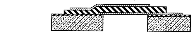
従来のFBARの構造として、図17のような構成がある。しかしながら良好な特性の薄膜圧電共振器を作製するのには次のような課題があった。
(1)基板裏面にキャビティを形成する際、基板の厚みがかなりあるため、キャビティ形成のためのエッチングを行うと、基板裏面の開口径と基板表面の開口径の大きさの違いが大きくなる(寸法変換差が大きくなる)。
(2)基板裏面のキャビティがそのまま薄膜圧電共振器を露出する構造となるため、基板裏面からの水分の浸入を防止することができない。
As a conventional FBAR structure, there is a structure as shown in FIG. However, the production of a thin film piezoelectric resonator having good characteristics has the following problems.
(1) When the cavity is formed on the back surface of the substrate, the thickness of the substrate is considerable. Therefore, when etching for forming the cavity is performed, the difference between the opening diameter on the back surface of the substrate and the opening diameter on the substrate surface increases. Dimensional conversion difference increases.)
(2) Since the cavity on the back surface of the substrate exposes the thin film piezoelectric resonator as it is, it is impossible to prevent moisture from entering from the back surface of the substrate.
このような問題点を解決するため、特許文献1のような構造が考えられている(図18参照)。図18において、空洞部206は比較的層厚の薄い第1の半導体層209に形成されるため、上記(1)のような、寸法変換差の問題が発生しにくい。また、空洞部6は半導体基板1上に形成されるため、薄膜圧電素子が露出することはなく、上記(2)の問題も生じにくい。
しかしながら、図18の構造は、以下の問題点がある。すなわち、半導体基板201上に圧電素子を形成した後、半導体基板201表面から空洞部206形成のためのエッチングを施さなければならない。そのため、空洞部206の横幅が大きくなり、第1の電極202、圧電体薄膜203、第2の電極204を支持力を大きく損なうことになり、ひいては薄膜圧電素子がスプリアス振動を起こす可能性が高くなるという問題点がある。
However, the structure of FIG. 18 has the following problems. That is, after a piezoelectric element is formed on the
本発明は上記の問題点を解決すべくなされたもので、スプリアス振動を起こす等の不具合を生ずることのない薄膜圧電共振器を得ることを目的とする。 The present invention has been made to solve the above-described problems, and an object of the present invention is to obtain a thin-film piezoelectric resonator that does not cause problems such as spurious vibrations.
上記の課題を解決するために本発明の薄膜圧電共振器は、表面、裏面を貫く第一の貫通孔が形成される第一の基板と、前記第一の基板下に載置される第二の基板と、前記貫通孔上に形成され、かつその幅が前記貫通孔の幅より大きい下部電極と、前記下部電極上に形成される圧電膜と、前記圧電膜上に形成される上部電極と、を具備し、前記貫通孔と前記第一の基板の表面とでキャビティを構成することを特徴とする。 In order to solve the above problems, a thin film piezoelectric resonator of the present invention includes a first substrate on which a first through hole penetrating a front surface and a back surface is formed, and a second substrate placed under the first substrate. A substrate, a lower electrode formed on the through hole and having a width larger than that of the through hole, a piezoelectric film formed on the lower electrode, and an upper electrode formed on the piezoelectric film, And a cavity is formed by the through hole and the surface of the first substrate.
また、本発明の薄膜圧電共振器の製造方法は、第一の基板表面に下部電極、圧電膜、上部電極を形成する工程と、前記第一の基板裏面からの気相エッチングにより、前記下部電極に達し、前記第一の基板を貫通する貫通孔を形成する工程と、前記第一の基板裏面に第二の基板を貼り合わせる工程とを具備することを特徴とする。 The method for manufacturing a thin film piezoelectric resonator according to the present invention includes the step of forming a lower electrode, a piezoelectric film, and an upper electrode on the surface of the first substrate, and vapor phase etching from the back surface of the first substrate. And forming a through-hole penetrating the first substrate, and bonding a second substrate to the back surface of the first substrate.
本発明によれば、キャビティを第一の基板の裏面からの異方性エッチングにより形成するため、キャビティの幅を所望の大きさにすることができる。従って、上部電極、圧電膜、下部電極の支持面積を大きくすることができるため、不要なスプリアス振動が生じにくくなる。 According to the present invention, since the cavity is formed by anisotropic etching from the back surface of the first substrate, the width of the cavity can be set to a desired size. Therefore, since the support area of the upper electrode, the piezoelectric film, and the lower electrode can be increased, unnecessary spurious vibration is less likely to occur.
本発明者らは裏面空洞型の薄膜圧電共振器の高性能化と実装パッケージ法について鋭意検討を行った。その結果、この目的のためには、パッケージを構成する層構造を最適化することが重要であることを見出した。ここで薄膜圧電共振器とはセラミック共振子やSAWデバイスとは異なり、薄膜の厚み方向の弾性波を用いた共振、すなわち薄膜をバルクとして膜全体の弾性波を用いた共振器のことである。以下図面を用いて詳細に説明する。 The present inventors diligently studied about the high performance of the back cavity type thin film piezoelectric resonator and the mounting package method. As a result, it has been found that for this purpose, it is important to optimize the layer structure constituting the package. Here, unlike a ceramic resonator or a SAW device, a thin film piezoelectric resonator is a resonance using an elastic wave in the thickness direction of the thin film, that is, a resonator using an elastic wave of the entire film as a bulk. This will be described in detail below with reference to the drawings.
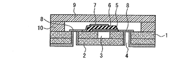
図1は本発明に係わる第1の実施例を示すものである。薄膜圧電共振器は、第一シリコン基板1上に形成され、下部電極5をAl、圧電体膜6をAlN、上部電極7をAlとする2枚の電極で挟み込み込まれた橋梁を共振させ共振特性を得るものである。下部電極5はAlNの配向性を高めるため、下層がアモルフォス構造となる二重構造となっている。AlNは配向制御することで、Q値(Quality factor:共振の鋭さを表す値)向上等の好特性を得る。スパッタで成膜した本実施例では配向性はX線のロッキングカーブで1.5゜以下に制御することができる。キャビティ3は第一シリコン基板1裏面側から反応性イオンエッチング(RIE)により基板をくり抜くことで形成される。電極パッド8は金(Au)、ビアホール4の内面もメッキによりAuで被覆されている。第二のシリコン基板2はその表面が清浄表面となっており、第二のシリコン基板2表面と第一のシリコン基板の裏面とが真空中にて直接接着による貼りあわせで形成される。上部電極7の上部にはこの薄膜圧電共振器をパッケージとした際の蓋に該当する第三のシリコン基板9が形成されており、この第三のシリコン基板9とシーリング(ガスケット)10、及び下部電極5、圧電体膜6、上部電極7からなる圧電共振器本体との間で中空が形成され、この中空と空洞3中に圧電共振器本体を配置することで、共振動作を生じさせることになる。ここで、キャビティ3の幅(図1紙面に平行な方向における幅)は、下部電極5の幅(図1紙面に平行な方向における幅)よりも小さくなっている。
FIG. 1 shows a first embodiment according to the present invention. The thin film piezoelectric resonator is formed on the
シーリング10により、第一のシリコン基板1と第三のシリコン基板9とが強力に接着されるため、その後のダイシング工程で剥がれるなどの問題も起きない。第二のシリコン基板2、第三のシリコン基板9は所望の仕様の厚さを維持する目的から200μm程度とすることが適当である。これらの厚さは実装時や製造時の要求により、第一のシリコン基板1の厚さよりもフレキシブルに設定することができる。
Since the
本構造において最適化したのは第一のシリコン基板1の厚さである。通常のシリコン基板厚である400〜600μmをRIEでエッチングすると、途中でオーバーハングやノッチ(エッチングに用いるマスクからの寸法差)が出る。そればかりでなく、エッチング時間も増加し、製造上大きな問題となる。そこで、基板の厚さを200μm以下とするとこれらの問題が激減することを発明者らの鋭意研究により見出した。この根拠を以下に示す。実用的なエッチングレートとして5μm以上を維持するとオーバーハングやノッチ量として深さ方向に対して1%以下に制御するのは難しい。裏面空洞の位置ずれは寄生容量を薄膜共振素子に作りつけてしまうために3μm以下とする必要があるが、これらの関係を満たすためにはマージンを考慮して200μm以下にする必要がある。
What is optimized in this structure is the thickness of the
図14に実際に基板厚を変えて行ったノッチ量に対する影響に関す実験結果を示す。この関係図に示すように200μm以下が適正なノッチ量範囲に制御するのに必須な基板厚となることがわかる。100μm以下にするとさらに制御性とスループットの上では望ましい。しかし基板が薄くなるため、取り扱いに関しては注意が必要となる。50μm前後が作製上の限界となる。 FIG. 14 shows the experimental results regarding the effect on the notch amount actually obtained by changing the substrate thickness. As shown in this relationship diagram, it can be seen that 200 μm or less is a substrate thickness that is essential for controlling the notch amount within an appropriate range. A thickness of 100 μm or less is desirable in terms of controllability and throughput. However, since the substrate becomes thin, care must be taken in handling. The manufacturing limit is around 50 μm.
図2乃至8に本実施例の製造方法を示す。まず、図2に示すように第一のシリコン基板1上にそれぞれアルミニウム(Al)等の材料からなる下部電極5、窒化アルミニウム(AlN)等の材料からなる圧電体膜6、アルミニウム(Al)等の材料からなる上部電極7となる材料を、10-7Torr以下に維持された真空チャンバーを有するスパッタ装置により、連続スパッタ法により成膜する。そしてアルゴン(Ar)等の不活性ガスで希釈されたCl2等の塩素系ガスを用いたドライエッチングにより、下部電極5、圧電体膜6、上部電極7をそれぞれ形成する。電極パッド8もこの段階でスパッタ法、ドライエッチングによるパターニングで形成する。
2 to 8 show the manufacturing method of this embodiment. First, as shown in FIG. 2, on the
次に、図3に示すように、上部構造側をシリンダー状の冶具に、例えば電子用ワックスを用いて接着し、AlNを含むスラリーにより第一のシリコン基板1裏面を、厚さ150μmとなるよう研磨する。
Next, as shown in FIG. 3, the upper structure side is bonded to a cylindrical jig using, for example, electronic wax, and the back surface of the
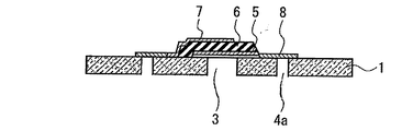
そして図4に示すように、冶具につけたまま、裏面空洞を、例えばボッシュシステムと呼ばれる、SF6系のガスを用いて、エッチングと堆積とを交互に繰り返すタイプの高速反応性イオンエッチング(高速RIE)により形成する。このとき、裏面空洞の幅(図1紙面に平行な方向における幅)は、下部電極5の幅(図1紙面に平行な方向における幅)よりも小さくなるようにエッチングする。エッチングレートは約10μm/minとする。 Then, as shown in FIG. 4, fast reactive ion etching (high-speed RIE) of a type in which etching and deposition are alternately repeated using an SF 6 -based gas called a Bosch system, for example, while the back cavity is attached to the jig. ). At this time, the etching is performed so that the width of the back cavity (width in the direction parallel to the paper surface of FIG. 1) is smaller than the width of the lower electrode 5 (width in the direction parallel to the paper surface of FIG. 1). The etching rate is about 10 μm / min.
高速RIE後、図5に示すように、底部となる第二のシリコン基板2を直接接着技術で貼りあわせる。直接接着とは清浄表面同士が真空中で原子層オーダで接触し、熱を加えることにより、原子間の結合が形成されることで接着する方法である。本実施例のような製造方法においては、例えば1kg/cm2の加重をかけ300℃の温度で行う。
After the high-speed RIE, as shown in FIG. 5, the
その後、図6に示すように、再度高速RIEを用いてビアホール4を形成し、図7に示すようにビアホール4内面から電極パッド8の裏面部にかけてメッキにてメタライズコートする。本実施例では、例えばNi、Auの積層構造を用いる。この段階で上部構造を冶具から剥離して、高周波パラメータ測定装置により、圧電薄膜共振子の共振周波数テストを行い、仕様に合うように周波数を調整する目的でトリミングを行う。トリミングは、例えば表面あるいは裏面より電極の一部をスパッタエッチングを行う方法で実施する。
Thereafter, as shown in FIG. 6, the via hole 4 is formed again by using high-speed RIE, and metallized by plating from the inner surface of the via hole 4 to the back surface of the
最後に、図8に示すように、感光性ポリイミドを第一のシリコン基板1上にスピンコートし、シーリング10となる部分をフォトリソグラフィ法で形成し、350℃程度でのキュアを行う。一方第三のシリコン基板9裏面にもポリイミドのスピンコートを施しておき、シーリング10との貼りあわせを行う。貼りあわせ後、再度350℃程度のキュアを行う。このキュアにより、シーリング10の成分となるポリイミドと、第三のシリコン基板10裏面にコートされたポリイミドとが強力に接着される。その後、パッケージ化された薄膜圧電共振器はダイシングして個片化されるが、この貼りあわせ方法によれば、ダイシング工程時にも第三のシリコン基板9が剥がれることはない。
Finally, as shown in FIG. 8, photosensitive polyimide is spin-coated on the
本実施例では基板はすべてシリコン基板としたが、ポリイミド基板等、樹脂製の基板を用いても良い。ただし、水分の浸透や透過性に関しては十分注意をはらう必要がある。またSi基板を用いる際も基板どうしの接着やシーリングとの接着に十分注意を払う必要がある。接着部が不十分であると、水分が浸透し、信頼性に関して深刻な課題となる。 In this embodiment, the substrate is a silicon substrate, but a resin substrate such as a polyimide substrate may be used. However, sufficient attention should be paid to moisture penetration and permeability. In addition, when using a Si substrate, it is necessary to pay sufficient attention to the bonding between the substrates and the sealing. If the bonded portion is insufficient, moisture penetrates and becomes a serious problem regarding reliability.
次に、本発明に係わる実施例2につき、図面を用いて説明する。図9は第2の実施例の薄膜圧電共振器の、第三のシリコン基板9を取り除いた状態での平面図、図10はA−A´における断面図(第三のシリコン基板9は接着された状態)である。本実施例の特徴は薄膜圧電共振器の空洞3の気圧と第三のシリコン基板9、シーリング10、薄膜圧電共振器本体とで取り囲まれた中空部分の気圧とが同一気圧になるように調整用の抜き穴11を、下部電極5、圧電体膜6、上部電極7を貫くように設けたことにある。その他符号が実施例1と同一の部分は同様な形状を有しているため、詳細な説明を省略する。
Next, a second embodiment according to the present invention will be described with reference to the drawings. FIG. 9 is a plan view of the thin film piezoelectric resonator of the second embodiment with the
実施例1のように空洞3と中空部分とが分離されている場合、製造時や使用時の温度環境などにより、それぞれの圧力が異なった場合、薄膜圧電共振子がたわみ、特性劣化が生じ、最悪の場合、薄膜圧電共振器自体が破壊されることもある。本実施例のように抜き穴を設けておくと、これらの問題は生じにくい。本実施例では下部電極5、圧電体膜6、上部電極7を貫くように直接抜き穴を設けたが、下部電極5、圧電体膜6、上部電極7を貫通せず、間接的に抜き穴を設けてもよい。本実施例では実施例1と比べて製造時の歩留まりが10%向上し、動作時の突発劣化も激減した。
When the
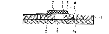
図11乃至13は本発明に係わる第3の実施例の製造方法を示すものである。実施例1における図3の工程までは同様である。本実施例の特徴は、図11に示すように、薄膜圧電共振器本体を冶具につけたまま、空洞3とビアホール4aを高速RIEにより同時にエッチングすることにある。空洞3の幅は実施例1と同様、下部電極5の幅よりも小さくなっている。この工程によりビアホールのエッチングの工程時間を大幅に短縮することが可能となる。
11 to 13 show a manufacturing method of the third embodiment according to the present invention. The process is the same up to the step of FIG. As shown in FIG. 11, this embodiment is characterized in that the
空洞3、ビアホール4aの同時エッチング後、図12に示すように、第一のシリコン基板1の裏面と第二のシリコン基板2の表面とを接着し、図13に示すように、再度RIEにより、ビアホール4aの形成位置に合わせ、ビアホール4aより開口径の大きいビアホール4bを高速RIE等の方法でエッチングする。本実施例によれば、ビアホール4aと4bとの位置合わせのマージンを大きくとることができ、もっとスループットの高いサンドブラストやレーザ加工などを併用することも可能となる。
After simultaneous etching of the
次に、以上の実施例により作成された薄膜圧電共振器のアプリケーションについて、図15、16を用いて説明する。 Next, the application of the thin film piezoelectric resonator produced by the above embodiment will be described with reference to FIGS.
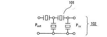
薄膜圧電共振器101は、図15に示すように直列ないし並列に複数個並べて梯子型フィルタ102を形成することにより、移動体通信機のRFフィルタとして利用することができる。
As shown in FIG. 15, the thin
また、図16に示すように、薄膜圧電共振器101、バリアブルキャパシタ104および増幅器105を組合せることで、移動体通信機の電圧制御発振器(Voltage Controlled Oscillator: VCO)103として 利用することができる。
Further, as shown in FIG. 16, by combining a thin
なお上記実施例における製造工程はそれぞれ単独で用いることも可能であるが、製造工程の一部をそれぞれ別の実施例の製造工程と組み合わせて用いてもさらに大きな効果を発揮することができる。 In addition, although the manufacturing process in the said Example can also be used individually, respectively, A bigger effect can be exhibited even if it uses a part of manufacturing process in combination with the manufacturing process of another Example, respectively.
1 … 第一のシリコン基板
2 … 第二のシリコン基板
3 … 空洞
4、4a、4b … ビアホール
5 … 下部電極
6 … 圧電体膜
7 … 上部電極
8 … 電極パッド
9 … 第三のシリコン基板
10 … シーリング
11 … 抜き穴
101 … 薄膜圧電共振器
102 … 梯子型フィルタ
103 … 電圧制御発振器(VCO)
104 … バリアブルキャパシタ
105 … 増幅器
201 … 半導体基板
202 … 第1の電極
203 … 圧電体薄膜
204 … 第2の電極
206 … 空洞部
DESCRIPTION OF
DESCRIPTION OF
Claims (7)
前記第一の基板下に載置される第二の基板と、
前記貫通孔上に形成され、かつその幅が前記貫通孔の幅より大きい下部電極と、
前記下部電極上に形成される圧電膜と、
前記圧電膜上に形成される上部電極と、
を具備し、
前記貫通孔と前記第一の基板の表面とでキャビティを構成することを特徴とする薄膜圧電共振器。 A first substrate on which a first through-hole penetrating the front surface and the back surface is formed;
A second substrate placed under the first substrate;
A lower electrode formed on the through hole and having a width larger than the width of the through hole;
A piezoelectric film formed on the lower electrode;
An upper electrode formed on the piezoelectric film;
Comprising
A thin film piezoelectric resonator comprising a cavity formed by the through hole and the surface of the first substrate.
前記第一の基板裏面からの気相エッチングにより、前記下部電極に達し、前記第一の基板を貫通する貫通孔を形成する工程と、
前記第一の基板裏面に第二の基板を貼り合わせる工程と
を具備することを特徴とする薄膜圧電共振器の製造方法。
Forming a lower electrode, a piezoelectric film, and an upper electrode on the surface of the first substrate;
A step of forming a through hole that reaches the lower electrode and penetrates the first substrate by vapor phase etching from the back surface of the first substrate;
A method of manufacturing a thin film piezoelectric resonator, comprising: bonding a second substrate to the back surface of the first substrate.
Priority Applications (1)
| Application Number | Priority Date | Filing Date | Title |
|---|---|---|---|
| JP2004108049A JP2005295250A (en) | 2004-03-31 | 2004-03-31 | Thin film piezoelectric resonator and manufacturing method thereof |
Applications Claiming Priority (1)
| Application Number | Priority Date | Filing Date | Title |
|---|---|---|---|
| JP2004108049A JP2005295250A (en) | 2004-03-31 | 2004-03-31 | Thin film piezoelectric resonator and manufacturing method thereof |
Publications (1)
| Publication Number | Publication Date |
|---|---|
| JP2005295250A true JP2005295250A (en) | 2005-10-20 |
Family
ID=35327687
Family Applications (1)
| Application Number | Title | Priority Date | Filing Date |
|---|---|---|---|
| JP2004108049A Pending JP2005295250A (en) | 2004-03-31 | 2004-03-31 | Thin film piezoelectric resonator and manufacturing method thereof |
Country Status (1)
| Country | Link |
|---|---|
| JP (1) | JP2005295250A (en) |
Cited By (19)
| Publication number | Priority date | Publication date | Assignee | Title |
|---|---|---|---|---|
| JP2007159116A (en) * | 2005-12-07 | 2007-06-21 | Samsung Electronics Co Ltd | System-on-chip structure having air cavity for isolating a plurality of elements from each other, duplexer, and manufacturing method thereof |
| WO2007148459A1 (en) * | 2006-06-20 | 2007-12-27 | National Institute Of Advanced Industrial Science And Technology | Dielectric structure and method for manufacturing same |
| JP2008042878A (en) * | 2006-07-07 | 2008-02-21 | Ngk Insulators Ltd | Piezoelectric thin film device |
| JP2008118480A (en) * | 2006-11-06 | 2008-05-22 | Fujitsu Media Device Kk | Piezoelectric thin film device and manufacturing method thereof |
| JP2009147238A (en) * | 2007-12-17 | 2009-07-02 | National Institute Of Advanced Industrial & Technology | Dielectric structure, method for manufacturing dielectric structure, pressure transfer method, and holding structure |
| JP2010141570A (en) * | 2008-12-11 | 2010-06-24 | Ube Ind Ltd | Piezoelectric thin film acoustic resonator, and manufacturing method of the same |
| JP2011138909A (en) * | 2009-12-28 | 2011-07-14 | Clean Venture 21 Corp | Photoelectric conversion element and method for manufacturing the same, and photoelectric conversion device and method for manufacturing the same |
| WO2011111732A1 (en) * | 2010-03-12 | 2011-09-15 | 北陸電気工業株式会社 | Manufacturing method for sensor element equipped with pzt film |
| US20120049976A1 (en) * | 2010-09-01 | 2012-03-01 | Samsung Electronics Co., Ltd. | Bulk acoustic wave resonator structure, a manufacturing method thereof, and a duplexer using the same |
| JP2012165132A (en) * | 2011-02-04 | 2012-08-30 | Taiyo Yuden Co Ltd | Method for manufacturing acoustic wave device |
| JP2018129561A (en) * | 2017-02-06 | 2018-08-16 | 新日本無線株式会社 | Method for manufacturing bulk elastic wave resonator |
| JP2018536157A (en) * | 2015-10-28 | 2018-12-06 | コーボ ユーエス,インコーポレイティド | Sensor device having a bulk acoustic wave (BAW) resonator and a fluid via penetrating the substrate |
| CN108964628A (en) * | 2017-05-18 | 2018-12-07 | 三星电机株式会社 | Bulk acoustic wave resonator |
| CN109470367A (en) * | 2018-11-12 | 2019-03-15 | 中国科学院长春光学精密机械与物理研究所 | A kind of preparation method of broadband uncooled infrared detector based on FBAR |
| JP2022518313A (en) * | 2019-12-31 | 2022-03-15 | 中芯集成電路(寧波)有限公司上海分公司 | Resonator and its formation method |
| CN114257193A (en) * | 2020-09-21 | 2022-03-29 | 中芯集成电路(宁波)有限公司上海分公司 | Method for manufacturing film bulk acoustic resonator and filter |
| JP2022137818A (en) * | 2021-03-09 | 2022-09-22 | 太陽誘電株式会社 | Elastic wave device and method for manufacturing the same, filter and multiplexer |
| JP2023071988A (en) * | 2019-07-19 | 2023-05-23 | 中芯集成電路(寧波)有限公司上海分公司 | BAW resonator packaging module and packaging method |
| WO2025070357A1 (en) * | 2023-09-26 | 2025-04-03 | 日東電工株式会社 | Baw resonator, baw device, and electronic apparatus |
-
2004
- 2004-03-31 JP JP2004108049A patent/JP2005295250A/en active Pending
Cited By (32)
| Publication number | Priority date | Publication date | Assignee | Title |
|---|---|---|---|---|
| JP2007159116A (en) * | 2005-12-07 | 2007-06-21 | Samsung Electronics Co Ltd | System-on-chip structure having air cavity for isolating a plurality of elements from each other, duplexer, and manufacturing method thereof |
| WO2007148459A1 (en) * | 2006-06-20 | 2007-12-27 | National Institute Of Advanced Industrial Science And Technology | Dielectric structure and method for manufacturing same |
| JP2008004572A (en) * | 2006-06-20 | 2008-01-10 | National Institute Of Advanced Industrial & Technology | Dielectric structure and manufacturing method thereof |
| JP2008042878A (en) * | 2006-07-07 | 2008-02-21 | Ngk Insulators Ltd | Piezoelectric thin film device |
| JP2008118480A (en) * | 2006-11-06 | 2008-05-22 | Fujitsu Media Device Kk | Piezoelectric thin film device and manufacturing method thereof |
| JP2009147238A (en) * | 2007-12-17 | 2009-07-02 | National Institute Of Advanced Industrial & Technology | Dielectric structure, method for manufacturing dielectric structure, pressure transfer method, and holding structure |
| JP2010141570A (en) * | 2008-12-11 | 2010-06-24 | Ube Ind Ltd | Piezoelectric thin film acoustic resonator, and manufacturing method of the same |
| JP2011138909A (en) * | 2009-12-28 | 2011-07-14 | Clean Venture 21 Corp | Photoelectric conversion element and method for manufacturing the same, and photoelectric conversion device and method for manufacturing the same |
| WO2011111732A1 (en) * | 2010-03-12 | 2011-09-15 | 北陸電気工業株式会社 | Manufacturing method for sensor element equipped with pzt film |
| KR101782447B1 (en) | 2010-03-12 | 2017-09-28 | 호쿠리쿠 덴키 고교 가부시키가이샤 | Manufacturing method for sensor element equipped with pzt film |
| CN102792477A (en) * | 2010-03-12 | 2012-11-21 | 北陆电气工业株式会社 | Manufacturing method of sensor element provided with PZT film |
| JP5100915B2 (en) * | 2010-03-12 | 2012-12-19 | 北陸電気工業株式会社 | Manufacturing method of sensor element provided with PZT film |
| CN102792477B (en) * | 2010-03-12 | 2015-05-27 | 北陆电气工业株式会社 | Manufacturing method of sensor element provided with PZT film |
| CN104752602A (en) * | 2010-03-12 | 2015-07-01 | 北陆电气工业株式会社 | Manufacturing method for sensor element equipped with PZT film |
| CN104752602B (en) * | 2010-03-12 | 2017-07-28 | 北陆电气工业株式会社 | Possesses the manufacture method of the sensor element of PZT film |
| US20120049976A1 (en) * | 2010-09-01 | 2012-03-01 | Samsung Electronics Co., Ltd. | Bulk acoustic wave resonator structure, a manufacturing method thereof, and a duplexer using the same |
| US8648671B2 (en) * | 2010-09-01 | 2014-02-11 | Samsung Electronics Co., Ltd. | Bulk acoustic wave resonator structure, a manufacturing method thereof, and a duplexer using the same |
| US9148107B2 (en) | 2011-02-04 | 2015-09-29 | Taiyo Yuden Co., Ltd. | Method for manufacturing acoustic wave device |
| JP2012165132A (en) * | 2011-02-04 | 2012-08-30 | Taiyo Yuden Co Ltd | Method for manufacturing acoustic wave device |
| JP2018536157A (en) * | 2015-10-28 | 2018-12-06 | コーボ ユーエス,インコーポレイティド | Sensor device having a bulk acoustic wave (BAW) resonator and a fluid via penetrating the substrate |
| JP2018129561A (en) * | 2017-02-06 | 2018-08-16 | 新日本無線株式会社 | Method for manufacturing bulk elastic wave resonator |
| CN108964628A (en) * | 2017-05-18 | 2018-12-07 | 三星电机株式会社 | Bulk acoustic wave resonator |
| CN109470367A (en) * | 2018-11-12 | 2019-03-15 | 中国科学院长春光学精密机械与物理研究所 | A kind of preparation method of broadband uncooled infrared detector based on FBAR |
| JP2023071988A (en) * | 2019-07-19 | 2023-05-23 | 中芯集成電路(寧波)有限公司上海分公司 | BAW resonator packaging module and packaging method |
| JP7557893B2 (en) | 2019-07-19 | 2024-09-30 | 中芯集成電路(寧波)有限公司上海分公司 | Packaging module and method for packaging a BAW resonator |
| US12506458B2 (en) | 2019-07-19 | 2025-12-23 | Ningbo Semiconductor International Corporation (Shanghai Branch) | Packaging module and packaging method of BAW resonator |
| JP7255910B2 (en) | 2019-12-31 | 2023-04-11 | 中芯集成電路(寧波)有限公司上海分公司 | Resonator and method of forming the same |
| JP2022518313A (en) * | 2019-12-31 | 2022-03-15 | 中芯集成電路(寧波)有限公司上海分公司 | Resonator and its formation method |
| CN114257193A (en) * | 2020-09-21 | 2022-03-29 | 中芯集成电路(宁波)有限公司上海分公司 | Method for manufacturing film bulk acoustic resonator and filter |
| JP2022137818A (en) * | 2021-03-09 | 2022-09-22 | 太陽誘電株式会社 | Elastic wave device and method for manufacturing the same, filter and multiplexer |
| JP7611007B2 (en) | 2021-03-09 | 2025-01-09 | 太陽誘電株式会社 | Acoustic wave device and its manufacturing method, filter and multiplexer |
| WO2025070357A1 (en) * | 2023-09-26 | 2025-04-03 | 日東電工株式会社 | Baw resonator, baw device, and electronic apparatus |
Similar Documents
| Publication | Publication Date | Title |
|---|---|---|
| JP2005295250A (en) | Thin film piezoelectric resonator and manufacturing method thereof | |
| US12088270B2 (en) | Transversely-excited film bulk acoustic resonator package and method | |
| KR100622955B1 (en) | Thin film bulk acoustic resonator and its manufacturing method | |
| CN114553170A (en) | Transverse excitation film bulk acoustic resonator with low thermal impedance | |
| US10784838B2 (en) | Air-gap type film bulk acoustic resonator and method of manufacturing the same | |
| EP1469599A2 (en) | Air gap type FBAR, duplexer using the FBAR, and fabricating methods thereof | |
| CN112039485A (en) | Thin film piezoelectric acoustic wave filter and manufacturing method thereof | |
| JP2003347884A (en) | Film bulk acoustic resonator element and manufacturing method thereof | |
| CN109687835B (en) | Film bulk acoustic resonator, manufacturing method thereof and filter | |
| CN111130490A (en) | Bulk acoustic wave resonator having electrode with void layer, method of manufacturing the same, filter, and electronic apparatus | |
| US20060202769A1 (en) | Piezoelectric thin film device and method of producing the same | |
| CN113630099B (en) | Bulk acoustic wave resonator and manufacturing method, component, filter and electronic device | |
| CN108566177A (en) | Rf-resonator and filter | |
| US7057477B2 (en) | Integration of FBAR filter(s) and on-chip inductors | |
| JP2005333644A (en) | Filter with built-in inductor, duplexer, and manufacturing method thereof | |
| EP1471636B1 (en) | Film bulk acoustic resonator having an air gap and a method for manufacturing the same | |
| JP3952464B2 (en) | Duplexer | |
| CN110544689B (en) | Active device and passive single crystal device and monolithic integration method in radio frequency front-end module | |
| US7417360B2 (en) | Piezoelectric resonator and method for producing the same | |
| JPH0964675A (en) | Piezoelectric resonator on sealed cavity and its preparation | |
| CN111327291A (en) | Bulk acoustic wave resonator and elastic wave filter device | |
| JP2005117665A (en) | Air gap type FBAR and method for manufacturing the same, filter and duplexer using the same | |
| CN1953175A (en) | Complex RF device and method for manufacturing the same | |
| JP2005110017A (en) | High frequency filter module and manufacturing method thereof | |
| KR102028719B1 (en) | Method for manufacturing FBAR |
Legal Events
| Date | Code | Title | Description |
|---|---|---|---|
| A977 | Report on retrieval |
Free format text: JAPANESE INTERMEDIATE CODE: A971007 Effective date: 20070213 |
|
| A131 | Notification of reasons for refusal |
Free format text: JAPANESE INTERMEDIATE CODE: A131 Effective date: 20070220 |
|
| A02 | Decision of refusal |
Free format text: JAPANESE INTERMEDIATE CODE: A02 Effective date: 20070803 |