JP2005295051A - FM demodulator - Google Patents
FM demodulator Download PDFInfo
- Publication number
- JP2005295051A JP2005295051A JP2004104988A JP2004104988A JP2005295051A JP 2005295051 A JP2005295051 A JP 2005295051A JP 2004104988 A JP2004104988 A JP 2004104988A JP 2004104988 A JP2004104988 A JP 2004104988A JP 2005295051 A JP2005295051 A JP 2005295051A
- Authority
- JP
- Japan
- Prior art keywords
- amplitude
- signal
- detector
- voltage amplitude
- frequency
- Prior art date
- Legal status (The legal status is an assumption and is not a legal conclusion. Google has not performed a legal analysis and makes no representation as to the accuracy of the status listed.)
- Pending
Links
Images
Landscapes
- Circuits Of Receivers In General (AREA)
Abstract
【課題】入力されFM信号の周波数の上限を延ばすことができる上に、低消費電力化、低価格化の実現を図ること。
【解決手段】電圧振幅検出器1は、入力されるFM信号の電圧振幅を検出する。減衰器2は、そのFM信号の振幅を周波数に比例させて低下させ、振幅が低下されたFM信号を出力する電圧振幅検出器3は、減衰器2で減衰されたFM信号の電圧振幅を検出する。振幅変化分検出器4は、電圧振幅検出器1で検出された振幅値と電圧振幅検出器3で検出された振幅値と比率を求め、この求めた比率の変化分に応じて時間軸上で変化する出力信号をFM復調信号として生成して出力する。
【選択図】 図1An object of the present invention is to extend the upper limit of the frequency of an input FM signal, and to realize low power consumption and low price.
A voltage amplitude detector 1 detects a voltage amplitude of an input FM signal. The attenuator 2 decreases the amplitude of the FM signal in proportion to the frequency, and the voltage amplitude detector 3 that outputs the FM signal with the amplitude reduced detects the voltage amplitude of the FM signal attenuated by the attenuator 2. To do. The amplitude change detector 4 obtains the amplitude value detected by the voltage amplitude detector 1 and the amplitude value and ratio detected by the voltage amplitude detector 3, and on the time axis according to the obtained change in the ratio. A changing output signal is generated and output as an FM demodulated signal.
[Selection] Figure 1
Description
本発明は、FM信号を復調するFM復調装置に関するものである。 The present invention relates to an FM demodulator that demodulates an FM signal.
従来のFM復調装置として、入力されたFM信号をパルスに変換するリミッタ回路と、このリミッタ回路が出力する信号の一方を遅延させる遅延回路と、リミッタ回路の出力する他方の信号とその遅延させた信号との論理積演算により得られる信号を出力するアンド回路と、このアンド回路の出力により復調信号を得る低域通過フィルタとから構成されるものが知られている(例えば、特許文献1参照)。
しかし、特許文献1に記載のFM復調装置では、トランジスタで構成されるアンド回路などを有し、パルスの論理演算が行われる。この場合に、パルスの幅はトランジスタの持つ容量成分に大きく影響され、FM信号の周波数が高くなると、FM復調装置としての機能が大幅に劣化する。このような不具合を解消するために、ガリウム砒素(GaAs)の電界効果トランジスタを使用するようにしても良いが、入力されるFM信号の周波数は5〔GHz〕程度が限界である。 However, the FM demodulator described in Patent Document 1 includes an AND circuit composed of transistors, and performs pulse logical operations. In this case, the width of the pulse is greatly influenced by the capacitance component of the transistor, and when the frequency of the FM signal is increased, the function as the FM demodulator is greatly deteriorated. In order to solve such a problem, a gallium arsenide (GaAs) field effect transistor may be used, but the frequency of the input FM signal is limited to about 5 [GHz].
さらに、遅延回路は、差動回路を数段直列に並べたものが一般的である。このような構成では、FM復調装置の面積、消費電力が大きくなってしまうという不具合がある。
そこで、本発明の目的は、上記の点に鑑み、入力されるFM信号の周波数の上限を延ばすことができる上に、低消費電力化、低価格化の実現が可能であるFM復調装置を提供することにある。
Further, the delay circuit is generally a series of several differential circuits arranged in series. With such a configuration, there is a problem that the area and power consumption of the FM demodulator increase.
In view of the above, an object of the present invention is to provide an FM demodulator that can extend the upper limit of the frequency of an input FM signal, and can achieve low power consumption and low price. There is to do.
上記の課題を解決し本発明の目的を達成するために、本発明は、以下のような構成からなる。
すなわち、本発明は、FM信号を入力し、そのFM信号の振幅を検出する第1振幅検出手段と、前記FM信号を入力し、そのFM信号の振幅を周波数に比例させて低下させる減衰手段と、前記減衰手段の出力の振幅を検出する第2振幅検出手段と、前記両振幅検出手段で検出された両振幅の変化分を検出し、この検出変化分に応じた信号を出力する振幅変化分検出手段と、を備えている。
In order to solve the above problems and achieve the object of the present invention, the present invention has the following configuration.
That is, the present invention includes a first amplitude detection means for inputting an FM signal and detecting the amplitude of the FM signal, and an attenuation means for inputting the FM signal and reducing the amplitude of the FM signal in proportion to the frequency. The second amplitude detecting means for detecting the amplitude of the output of the attenuating means, and the change in amplitude detected by the two amplitude detecting means, and a signal corresponding to the detected change is output. Detecting means.
以上のような構成からなる本発明によれば、入力されるFM信号の周波数の上限を延ばすことができる上に、低消費電力化、低価格化の実現が可能である。 According to the present invention configured as described above, it is possible to extend the upper limit of the frequency of the input FM signal, and to realize low power consumption and low price.
以下、本発明の実施形態について、図面を参照して説明する。
本発明のFM復調装置の実施形態の構成について、図1および図2を参照して説明する。
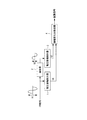
この実施形態に係るFM復調装置は、図1に示すように、電圧振幅検出器1と、減衰器2と、電圧振幅検出器3と、振幅変化分検出器4とを備えている。
Hereinafter, embodiments of the present invention will be described with reference to the drawings.
The configuration of the embodiment of the FM demodulator of the present invention will be described with reference to FIGS.
As shown in FIG. 1, the FM demodulator according to this embodiment includes a voltage amplitude detector 1, an
電圧振幅検出器1は、入力されるFM信号の振幅(電圧振幅)を検出するものである。この電圧振幅検出器1は、入力されるFM信号の振幅が、図1に示すようにピーク・ピーク値でV1の場合には、そのピーク・ピーク値を検出するのが好ましい。
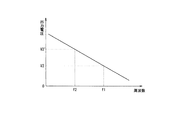
減衰器2は、FM信号を入力し、このFM信号の振幅を周波数に比例させて低下させ、振幅が低下されたFM信号を出力するものである。この減衰器2の周波数特性(周波数−出力電圧特性)の一例を示すと、図2に示すようになる。この減衰器2は、例えば、図2に示すような特性を有する伝送路などから構成される。
The voltage amplitude detector 1 detects the amplitude (voltage amplitude) of the input FM signal. This voltage amplitude detector 1 preferably detects the peak-peak value when the amplitude of the input FM signal is a peak-peak value V1 as shown in FIG.
The
電圧振幅検出器3は、減衰器2で減衰されたFM信号の振幅(電圧振幅)を検出するものである。この電圧振幅検出器3は、減衰器2の出力信号の振幅が、図1に示すようにピーク・ピーク値でV2の場合には、そのピーク・ピーク値を検出するのが好ましい。
振幅変化分検出器4は、電圧振幅検出器1で検出された振幅値と電圧振幅検出器3で検出された振幅値と比率を求め、この求めた比率の変化分に応じて時間軸上で変化(増減)する出力信号をFM復調信号として生成して出力するものである。
The
The
次に、このような構成からなる実施形態の動作例について、図1および図2を参照して説明する。
図1に示すように、例えば、いま入力されるFM信号の周波数をf1、その振幅をV1とする。この場合に、そのFM信号は、電圧振幅検出器1と減衰器2とにそれぞれ入力される。
Next, an operation example of the embodiment having such a configuration will be described with reference to FIGS. 1 and 2.
As shown in FIG. 1, for example, the frequency of the FM signal input now is f1, and its amplitude is V1. In this case, the FM signal is input to the voltage amplitude detector 1 and the
そのFM信号は、電圧振幅検出器1にそのまま入力されてその振幅値が検出される。このため、電圧振幅検出器1が検出する検出値はV1となり、これが振幅変化分検出器4に入力される。
一方、減衰器2に入力されるFM信号は、その周波数f1に従ってその振幅はV2に低下し(図1および図2参照)、これが電圧振幅検出器3に入力されてその振幅値が検出される。このため、電圧振幅検出器3が検出する検出値はV2となり、これが振幅変化分検出器4に入力される。
The FM signal is inputted as it is to the voltage amplitude detector 1 and its amplitude value is detected. For this reason, the detected value detected by the voltage amplitude detector 1 is V1, and this is input to the
On the other hand, the amplitude of the FM signal input to the
振幅変化分検出器4では、その検出値V1と検出値V2との比率V2/V1を求め、この求めた比率に応じた信号を生成して出力する。
次に、入力されるFM信号の振幅がV1のままで周波数がf1からf2に変化(低下)したものとする(f1>f2)。
この場合には、電圧振幅検出器1が検出する検出値はV1で変化せず、これが振幅変化分検出器4に入力される。
In the
Next, it is assumed that the frequency of the input FM signal is changed (decreased) from f1 to f2 while the amplitude of the FM signal remains V1 (f1> f2).
In this case, the detection value detected by the voltage amplitude detector 1 does not change at V 1 and is input to the
一方、減衰器2からの出力は、FM信号の周波数がf1からf2に変化したことに伴ない、その振幅がV2からV2’に増加し(図2参照)、これが電圧振幅検出器3に入力されてその振幅値が検出される。従って、電圧振幅検出器3が検出する検出値はV2からV2’に変化し、これが振幅変化分検出器4に入力される。
このため、振幅変化分検出器4が検出する比率は、V2/V1からV2’/V1に変化し、この変化に応じて生成される出力信号も時間軸上で変化(増減)する。従って、振幅変化分検出器4から出力される出力信号は、FM信号が復調された復調信号となる。
On the other hand, the output from the
For this reason, the ratio detected by the
ここで、減衰器1の出力特性は、図2に示すように周波数に比例するようになっている。このため、FM信号の周波数f1,f2の関係がf1=2×f2とすると、次の(1)式の関係が成り立つ。
2×(V2/V1)=(V2’/V1)・・・(1)
(1)式によれば、FM信号の周波数がf1からf2に変化(低下)して1/2になると、振幅変化分検出器4が求める上記の比率は2倍に変化する。従って、振幅変化分検出器4では、その比率の大幅な変化を利用して時間軸上で変化する信号を容易に生成することができる。
Here, the output characteristic of the attenuator 1 is proportional to the frequency as shown in FIG. Therefore, if the relationship between the frequencies f1 and f2 of the FM signal is f1 = 2 × f2, the relationship of the following equation (1) is established.
2 × (V2 / V1) = (V2 ′ / V1) (1)
According to the equation (1), when the frequency of the FM signal changes (decreases) from f1 to f2 and becomes 1/2, the above-mentioned ratio obtained by the
以上説明したように、この実施形態によれば、入力されFM信号の周波数の上限を延ばすことができる上に、低消費電力化、低価格化の実現が可能である。
なお、図1に示す振幅変化分検出器4では、電圧振幅検出器1と電圧振幅検出器3とで検出された両振幅値の比率を求め、この求めた比率の変化分に応じて時間軸上で変化する出力信号をFM復調信号として生成出力するようにした。
As described above, according to this embodiment, it is possible to extend the upper limit of the frequency of the input FM signal, and it is possible to realize low power consumption and low price.
In the
しかし、これに代えて、電圧振幅検出器1と電圧振幅検出器3とで検出された両振幅値の差分を求め、この求めた差分に応じて時間軸上で変化する出力信号をFM復調信号として生成出力するようにしても良い。
However, instead of this, a difference between both amplitude values detected by the voltage amplitude detector 1 and the
1・・・電圧振幅検出器、2・・・減衰器、3・・・電圧振幅検出器、4・・・振幅変化分検出器。 DESCRIPTION OF SYMBOLS 1 ... Voltage amplitude detector, 2 ... Attenuator, 3 ... Voltage amplitude detector, 4 ... Amplitude change detector.
Claims (1)
前記FM信号を入力し、そのFM信号の振幅を周波数に比例させて低下させる減衰手段と、
前記減衰手段の出力の振幅を検出する第2振幅検出手段と、
前記両振幅検出手段で検出された両振幅の変化分を検出し、この検出変化分に応じた信号を出力する振幅変化分検出手段と、
を備えていることを特徴とするFM復調装置。 First amplitude detection means for inputting an FM signal and detecting the amplitude of the FM signal;
Attenuating means for inputting the FM signal and reducing the amplitude of the FM signal in proportion to the frequency;
Second amplitude detection means for detecting the amplitude of the output of the attenuation means;
Amplitude change detecting means for detecting a change in both amplitudes detected by the both amplitude detecting means and outputting a signal corresponding to the detected change;
An FM demodulator characterized by comprising:
Priority Applications (1)
| Application Number | Priority Date | Filing Date | Title |
|---|---|---|---|
| JP2004104988A JP2005295051A (en) | 2004-03-31 | 2004-03-31 | FM demodulator |
Applications Claiming Priority (1)
| Application Number | Priority Date | Filing Date | Title |
|---|---|---|---|
| JP2004104988A JP2005295051A (en) | 2004-03-31 | 2004-03-31 | FM demodulator |
Publications (1)
| Publication Number | Publication Date |
|---|---|
| JP2005295051A true JP2005295051A (en) | 2005-10-20 |
Family
ID=35327528
Family Applications (1)
| Application Number | Title | Priority Date | Filing Date |
|---|---|---|---|
| JP2004104988A Pending JP2005295051A (en) | 2004-03-31 | 2004-03-31 | FM demodulator |
Country Status (1)
| Country | Link |
|---|---|
| JP (1) | JP2005295051A (en) |
Cited By (1)
| Publication number | Priority date | Publication date | Assignee | Title |
|---|---|---|---|---|
| US9172425B2 (en) | 2012-08-14 | 2015-10-27 | Samsung Electronics Co., Ltd. | Apparatus and method for ultra wideband communication using dual band pass filter |
-
2004
- 2004-03-31 JP JP2004104988A patent/JP2005295051A/en active Pending
Cited By (1)
| Publication number | Priority date | Publication date | Assignee | Title |
|---|---|---|---|---|
| US9172425B2 (en) | 2012-08-14 | 2015-10-27 | Samsung Electronics Co., Ltd. | Apparatus and method for ultra wideband communication using dual band pass filter |
Similar Documents
| Publication | Publication Date | Title |
|---|---|---|
| US7791390B2 (en) | Phase shifter | |
| US9106299B2 (en) | Audio signal processing circuit | |
| US7729679B1 (en) | Dynamic bandwidth filter for an FM receiver | |
| US10063214B2 (en) | Programmable band-pass filter circuit of analog front-end used for capacitance detection | |
| US20070273413A1 (en) | Clock buffer | |
| KR950022041A (en) | Pulse noise canceller in FM tuner | |
| CN1938957A (en) | Noise removing circuit | |
| US5708375A (en) | Minimum pulse width detector for a measurement instrument | |
| US4438405A (en) | Frequency discriminating device | |
| JP2006191180A (en) | Optical receiver | |
| US20060100726A1 (en) | Digital audio amplifier, an audio system including the same, and a method of amplifying an audio signal | |
| JP2004297137A (en) | Receiver | |
| US9923646B1 (en) | Combination low-pass filter | |
| JP2005204037A (en) | Noise-eliminating device | |
| US5828238A (en) | Digital frequency discriminator | |
| US20060111073A1 (en) | Demodulator of frequency modulated signals, and demodulating method of frequency modulated signals | |
| JP3585417B2 (en) | Receiving machine | |
| JP5643782B2 (en) | Receiving machine | |
| JPS6373720A (en) | Receiving machine | |
| JP3617788B2 (en) | FM receiver | |
| JP2692394B2 (en) | Phase frequency comparator | |
| JP6551879B2 (en) | Detection sensor | |
| JP2010154048A (en) | Harmonic mixer circuit, and method of preventing characteristic degradation | |
| JPH0210976A (en) | Pilot signal discrimination circuit | |
| JPH066140A (en) | Voice detection circuit |