JP2005294891A - Surface acoustic wave device - Google Patents
Surface acoustic wave device Download PDFInfo
- Publication number
- JP2005294891A JP2005294891A JP2004102471A JP2004102471A JP2005294891A JP 2005294891 A JP2005294891 A JP 2005294891A JP 2004102471 A JP2004102471 A JP 2004102471A JP 2004102471 A JP2004102471 A JP 2004102471A JP 2005294891 A JP2005294891 A JP 2005294891A
- Authority
- JP
- Japan
- Prior art keywords
- surface acoustic
- acoustic wave
- longitudinally coupled
- resonator type
- coupled resonator
- Prior art date
- Legal status (The legal status is an assumption and is not a legal conclusion. Google has not performed a legal analysis and makes no representation as to the accuracy of the status listed.)
- Granted
Links
- 238000010897 surface acoustic wave method Methods 0.000 title claims abstract description 313
- 239000000758 substrate Substances 0.000 claims abstract description 104
- 238000004891 communication Methods 0.000 claims description 9
- 238000010586 diagram Methods 0.000 description 17
- 238000006243 chemical reaction Methods 0.000 description 13
- 238000012986 modification Methods 0.000 description 11
- 230000004048 modification Effects 0.000 description 11
- 230000000052 comparative effect Effects 0.000 description 8
- 230000005540 biological transmission Effects 0.000 description 7
- 238000013461 design Methods 0.000 description 7
- 238000000034 method Methods 0.000 description 7
- 229910013641 LiNbO 3 Inorganic materials 0.000 description 2
- 238000003780 insertion Methods 0.000 description 2
- 230000037431 insertion Effects 0.000 description 2
- 239000011347 resin Substances 0.000 description 2
- 229920005989 resin Polymers 0.000 description 2
- 238000012546 transfer Methods 0.000 description 2
- 230000008901 benefit Effects 0.000 description 1
- 230000008878 coupling Effects 0.000 description 1
- 238000010168 coupling process Methods 0.000 description 1
- 238000005859 coupling reaction Methods 0.000 description 1
- 238000011161 development Methods 0.000 description 1
- 230000000694 effects Effects 0.000 description 1
- 239000000463 material Substances 0.000 description 1
- 230000001902 propagating effect Effects 0.000 description 1
- 230000009467 reduction Effects 0.000 description 1
- 238000007789 sealing Methods 0.000 description 1
Images


Landscapes
- Surface Acoustic Wave Elements And Circuit Networks Thereof (AREA)
Abstract
Description
本発明は弾性表面波装置に関し、詳しくは、位相が反転した2つの平衡信号を出力する弾性表面波装置に関する。 The present invention relates to a surface acoustic wave device, and more particularly, to a surface acoustic wave device that outputs two balanced signals whose phases are inverted.
近年の携帯電話機の小型化、軽量化に対する技術的進歩は目覚しいものがある。これを実現するための手段として、各構成部品の削減、小型化はもとより、複数の機能を複合した部品の開発も進んできた。このような状況を背景に、携帯電話機のRF段に使用する弾性表面波フィルタに平衡−不平衡変換機能、いわゆるバランの機能を持たせたものも近年盛んに研究され、GSMなどを中心に使用されるようになってきた。このような平衡−不平衡変換機能を持たせた弾性表面波装置に関して、種々提案されている。 In recent years, there has been a remarkable technological advance in reducing the size and weight of mobile phones. As means for realizing this, not only the reduction and miniaturization of each component, but also the development of a component combining a plurality of functions has progressed. Against this backdrop, a surface acoustic wave filter used in the RF stage of a mobile phone, which has a balanced-unbalanced conversion function, that is, a so-called balun function, has been actively studied in recent years, and is mainly used for GSM. It has come to be. Various surface acoustic wave devices having such a balance-unbalance conversion function have been proposed.
例えば図1に、不平衡信号端子側のインピーダンスが50Ω、平衡信号端子側のインピーダンスが200Ωの平衡−不平衡変換機能を持たせた弾性表面波装置の素子構成を示す。この弾性表面波装置は、3つのIDTおよびそれらを挟み込むように設けられたリフレクタを有する弾性表面波フィルタ101〜104を用い、前記弾性表面波フィルタ101と102、前記弾性表面波フィルタ103と104をそれぞれ縦続接続し、前記弾性表面波フィルタ101と103を電気的に並列接続されるように不平衡信号端子105と接続し、前記弾性表面波フィルタ102と104を直列接続されるようにそれぞれ平衡信号端子106,107と接続している。その際、弾性表面波フィルタ104は、他の3つの弾性表面波フィルタに対して伝送位相特性が約180度異なるように中央部のIDTが反転されている。これにより平衡−不平衡変換機能を持たせることができ、さらに平衡信号端子側のインピーダンスは、不平衡信号端子側のインピ−ダンスの約4倍とすることができる(例えば、特許文献1参照)。
For example, FIG. 1 shows an element configuration of a surface acoustic wave device having a balanced-unbalanced conversion function in which the impedance on the unbalanced signal terminal side is 50Ω and the impedance on the balanced signal terminal side is 200Ω. This surface acoustic wave device uses surface
平衡−不平衡変換機能を有し、かつ平衡信号端子側のインピーダンスが不平衡信号端子側のインピーダンスの約4倍となる構成としては、他にも図2や図3の構成が挙げられるが、図1の構成は図2、図3の構成に対して縦結合共振子型弾性表面波フィルタの交叉幅が半分であり、かつ不平衡信号端子側では2つの縦結合共振子型弾性表面波フィルタを並列接続していることより、フィルタの抵抗損が小さいというメリットがあり、低損失なフィルタを実現することができる。
平衡−不平衡変換機能を有するフィルタにおいては、不平衡信号端子と平衡信号端子のそれぞれの端子との間の通過帯域内での伝送特性において、振幅特性が等しく、かつ位相が180度反転していることが要求され、それぞれ振幅平衡度及び位相平衡度と呼んでいる。 In a filter having a balanced-unbalanced conversion function, the amplitude characteristics are equal and the phase is inverted by 180 degrees in the transmission characteristics in the passband between the unbalanced signal terminal and each terminal of the balanced signal terminal. These are called amplitude balance and phase balance, respectively.
振幅平衡度及び位相平衡度とは、前記平衡−不平衡変換機能を有するフィルタ装置を3ポートのデバイスと考え、例えば不平衡入力端子をポート1、平衡出力端子のそれぞれをポート2、ポート3としたとき、振幅平衡度と位相平衡度を、次のように定義される。
振幅平衡度=│A│
ただし、A=│20log(S21)│−│20log(S31)│
位相平衡度=│B−180│
ただし、B=│∠S21−∠S31│
なお、S21はポート1からポート2への伝達係数であり、S31はポート1からポート3への伝達係数である。
For the amplitude balance and the phase balance, the filter device having the balance-unbalance conversion function is regarded as a three-port device. For example, the unbalanced input terminal is
Amplitude balance = │A│
However, A = │20log (S21) │-│20log (S31) │
Phase balance = | B-180 |
However, B = │∠S21-∠S31│
S21 is a transfer coefficient from
このような平衡度は、理想的には、フィルタの通過帯域内で、振幅平衡度は0dB、位相平衡度は0度とされる必要がある。 Ideally, such a degree of balance should be 0 dB for the amplitude balance and 0 degree for the phase balance within the passband of the filter.
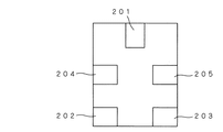
従来、圧電基板上に実際に図1のフィルタを構成する場合、図4のように2つのフィルタが弾性表面波の伝搬方向に隣り合うように構成していた。これは平衡信号端子の振幅平衡度、位相平衡度を悪化させないように仮想中心軸Aに対して左右対称にレイアウトするためである。その場合、弾性表面波装置のパッケージの裏面端子は図5のようにされていた。図5において端子201が不平衡信号端子、端子202,203が平衡信号端子、端子204,205,206がアース端子である。つまり不平衡信号端子201(入力端子)を上として見た場合、横長となる構成である。
Conventionally, when the filter of FIG. 1 is actually formed on a piezoelectric substrate, the two filters are adjacent to each other in the propagation direction of the surface acoustic wave as shown in FIG. This is for laying out symmetrically with respect to the virtual center axis A so as not to deteriorate the amplitude balance and the phase balance of the balanced signal terminal. In this case, the back terminal of the surface acoustic wave device package is as shown in FIG. In FIG. 5, a
一方で近年、図6や図7のように、不平衡信号端子105(入力端子)を上としてみた場合に、パッケージが縦長となる構成が望まれている。これは近年、1つの携帯電話に複数の方式を取り込む場合が多いため、実際の携帯電話セットで複数の弾性表面波装置を横に並べた場合、縦長の構成の方が実装上、有利となるためである。 On the other hand, in recent years, as shown in FIGS. 6 and 7, when the unbalanced signal terminal 105 (input terminal) is viewed upward, a configuration in which the package is vertically long is desired. In recent years, there are many cases in which a plurality of methods are incorporated into one mobile phone. Therefore, when a plurality of surface acoustic wave devices are arranged side by side in an actual mobile phone set, a vertically long configuration is advantageous in terms of mounting. Because.
しかし図4のような圧電基板のレイアウトで縦長の構成とすると、2つのフィルタを隣り合うように構成しているので、この2つのフィルタの素子長で短辺側の寸法が決まってしまい、市場要求に合った小型化に対応できない。また、図8のように素子をずらして対応しようとすると、仮想中心軸Aに対して左右非対称な構成となってしまい、平衡信号端子間の平衡度が悪化してしまうという欠点があった。 However, if the piezoelectric substrate layout as shown in FIG. 4 is a vertically long configuration, the two filters are configured to be adjacent to each other. Therefore, the element length of the two filters determines the dimensions on the short side. Cannot meet the demands for miniaturization. Further, when trying to respond by shifting the elements as shown in FIG. 8, the configuration becomes asymmetrical with respect to the virtual central axis A, and there is a disadvantage that the balance between the balanced signal terminals deteriorates.
すなわち、図4では、圧電基板上に、4つの縦結合共振子型弾性表面波フィルタを2行2列で配置し、不平衡信号端子(入力)が1つの長辺に、平衡信号端子(出力)が他の1つの長辺側に配置されている。マルチバンド携帯電話では、2つ以上の受信側弾性表面波フィルタをスイッチで切り替えて使用しており、高周波回路では配線を極力短くしなくてはならないので、2つの受信側弾性表面波フィルタの入力端子とスイッチ端子との距離も等しくかつ短くする必要がある。平衡信号端子(出力)が長辺に沿って配置される弾性表面波装置を2つ用いる場合、長辺方向に並べる必要があり、プリント基板上の面積はさらに横長となり、スペース効率がよくない。そこで、4素子の不平衡−平衡弾性表面波フィルタにおいて、縦長形状の圧電基板の上に、4つの縦結合共振子型弾性表面波フィルタをどのように配置するかが課題になる。共振子付き2素子の不平衡−平衡弾性表面波フィルタ、4素子の平衡−平衡弾性表面波フィルタ、共振子付き2素子の平衡−平衡弾性表面波フィルタについても、同様の課題がある。 That is, in FIG. 4, four longitudinally coupled resonator type surface acoustic wave filters are arranged in two rows and two columns on a piezoelectric substrate, an unbalanced signal terminal (input) is placed on one long side, and a balanced signal terminal (output) ) Is arranged on the other long side. In multiband mobile phones, two or more receiving surface acoustic wave filters are used by switching them. In high frequency circuits, the wiring must be as short as possible. The distance between the terminal and the switch terminal must be equal and short. When two surface acoustic wave devices in which balanced signal terminals (outputs) are arranged along the long side are used, they need to be arranged in the long side direction, and the area on the printed circuit board becomes further horizontally long, so that the space efficiency is not good. Therefore, in the four-element unbalanced-balanced surface acoustic wave filter, how to arrange the four longitudinally coupled resonator type surface acoustic wave filters on the vertically long piezoelectric substrate becomes a problem. The same problem occurs in the two-element unbalanced-balanced surface acoustic wave filter with the resonator, the four-element balanced-balanced surface acoustic wave filter, and the two-element balanced-balanced surface acoustic wave filter with the resonator.
本発明は、このような実情に鑑みて、平衡度が良好で、弾性表面波装置を実装する回路基板の小型化に好適な構成とすることができる、弾性表面波装置を提供することを目的とする。 SUMMARY OF THE INVENTION In view of such circumstances, the present invention has an object to provide a surface acoustic wave device that has a good balance and can be made suitable for downsizing a circuit board on which the surface acoustic wave device is mounted. And
本発明は、上記課題を解決するために、以下のように構成した弾性表面波装置を提供する。 In order to solve the above-mentioned problems, the present invention provides a surface acoustic wave device configured as follows.
弾性表面波装置は、長方形の圧電基板上に、弾性表面波の伝搬方向に沿って配置された3つのIDTをそれぞれ有する第1乃至第4の縦結合共振子型弾性表面波フィルタと、前記第1の縦結合共振子型弾性表面波フィルタの中央に配置された前記IDTの一端と、前記第3の縦結合共振子型弾性表面波フィルタの中央に配置された前記IDTの一端とに電気的に接続された第1の端子と、前記第2の縦結合共振子型弾性表面波フィルタの中央に配置された前記IDTの一端に電気的に接続された第2の端子と、前記第4の縦結合共振子型弾性表面波フィルタの中央に配置された前記IDTの一端に電気的に接続された第3の端子とが形成され、前記第1の縦結合共振子型弾性表面波フィルタと前記第2の縦結合共振子型弾性表面波フィルタとが縦続接続され、前記第3の縦結合共振子型弾性表面波フィルタと前記第4の縦結合共振子型弾性表面波フィルタが縦続接続され、前記第1乃至第4の縦結合共振子型弾性表面波フィルタのうち1つの位相が他の3つの位相と180度異なる、素子チップを備える。前記第1乃至第4の縦結合共振子型弾性表面波フィルタは、それぞれの弾性表面波の伝搬方向が前記圧電基板の長辺と平行な方向となるように、前記圧電基板の短辺と平行な方向に並べて配置される。 The surface acoustic wave device includes first to fourth longitudinally coupled resonator type surface acoustic wave filters each having three IDTs arranged along a propagation direction of the surface acoustic wave on a rectangular piezoelectric substrate; Electrically connected to one end of the IDT disposed at the center of one longitudinally coupled resonator type surface acoustic wave filter and one end of the IDT disposed at the center of the third longitudinally coupled resonator type surface acoustic wave filter A second terminal electrically connected to one end of the IDT disposed in the center of the second longitudinally coupled resonator-type surface acoustic wave filter, and the fourth terminal A third terminal electrically connected to one end of the IDT disposed in the center of the longitudinally coupled resonator type surface acoustic wave filter; and the first longitudinally coupled resonator type surface acoustic wave filter and the A second longitudinally coupled resonator type surface acoustic wave filter; The third longitudinally coupled resonator type surface acoustic wave filter and the fourth longitudinally coupled resonator type surface acoustic wave filter are cascaded, and the first to fourth longitudinally coupled resonator type surface acoustic waves are cascaded. An element chip is provided in which one phase of the wave filter is 180 degrees different from the other three phases. The first to fourth longitudinally coupled resonator type surface acoustic wave filters are parallel to the short sides of the piezoelectric substrate so that the propagation directions of the respective surface acoustic waves are parallel to the long sides of the piezoelectric substrate. Are arranged side by side.
上記構成において、第1の端子に不平衡信号を入力すると、位相が反転した2つの平衡信号が第2及び第3端子からそれぞれ出力される。第1の端子に対して第1及び第3の縦結合共振子型弾性表面波フィルタを並列に接続し、第2及び第3端子の間に第2及び第4の縦結合共振子型弾性表面波フィルタを直列に接続することにより、インピーダンス変換機能を有するようにすることができる。 In the above configuration, when an unbalanced signal is input to the first terminal, two balanced signals having inverted phases are output from the second and third terminals, respectively. The first and third longitudinally coupled resonator type surface acoustic wave filters are connected in parallel to the first terminal, and the second and fourth longitudinally coupled resonator type elastic surfaces are interposed between the second and third terminals. By connecting wave filters in series, an impedance conversion function can be provided.
上記構成によれば、第1乃至第4の縦結合共振子型弾性表面波フィルタを圧電基板上に対称に配置して、平衡度を改善することができる。また、圧電基板の一方の短辺側に、不平衡信号を入力する第1の端子が配置され、圧電基板の他方の短辺側に、平衡信号を出力する第2及び第3の端子が配置されるので、出力端子や入力端子を狭い範囲に集約することができる縦長パッケージへの実装が容易となる。 According to the above configuration, the first to fourth longitudinally coupled resonator type surface acoustic wave filters can be arranged symmetrically on the piezoelectric substrate to improve the balance. In addition, a first terminal for inputting an unbalanced signal is arranged on one short side of the piezoelectric substrate, and a second and a third terminal for outputting a balanced signal are arranged on the other short side of the piezoelectric substrate. Therefore, it becomes easy to mount on a vertically long package that can collect output terminals and input terminals in a narrow range.
また、本発明は、上記課題を解決するために、以下のように構成した弾性表面波装置を提供する。 In order to solve the above-mentioned problems, the present invention provides a surface acoustic wave device configured as follows.
弾性表面波装置は、長方形の圧電基板上に、弾性表面波の伝搬方向に沿って配置された3つのIDTをそれぞれ有する第1及び第2の縦結合共振子型弾性表面波フィルタと、1つのIDTをそれぞれ有する第1及び第2の弾性表面波共振子と、前記第1の縦結合共振子型弾性表面波フィルタの中央に配置された前記IDTの一端と、前記第2の縦結合共振子型弾性表面波フィルタの中央に配置された前記IDTの一端とに電気的に接続された第1の端子と、前記第1の弾性表面波共振子の前記IDTの一端に電気的に接続された第2の端子と、前記第2の弾性表面波共振子の前記IDTの一端に電気的に接続された第3の端子とが形成され、前記第1の縦結合共振子型弾性表面波フィルタの両側に配置された前記IDTのそれぞれの一端が、前記第1の弾性表面波共振子の前記IDTの他端に接続され、前記第2の縦結合共振子型弾性表面波フィルタの両側に配置された前記IDTのそれぞれの一端が、前記第2の弾性表面波共振子の前記IDTの他端に接続され、前記第1及び第2の縦結合共振子型弾性表面波フィルタの位相が180度異なる、素子チップを備える。前記第1及び第2の縦結合共振子型弾性表面波フィルタと前記第1及び第2の弾性表面波共振子は、それぞれの弾性表面波の伝搬方向が前記圧電基板の長辺と平行な方向となるように、前記圧電基板の短辺と平行な方向に並べて配置される。 The surface acoustic wave device includes first and second longitudinally coupled resonator type surface acoustic wave filters each having three IDTs arranged along a propagation direction of the surface acoustic wave on a rectangular piezoelectric substrate, and one First and second surface acoustic wave resonators each having an IDT, one end of the IDT disposed in the center of the first longitudinally coupled resonator type surface acoustic wave filter, and the second longitudinally coupled resonator A first terminal electrically connected to one end of the IDT disposed at the center of the surface acoustic wave filter, and one end electrically connected to one end of the IDT of the first surface acoustic wave resonator A second terminal and a third terminal electrically connected to one end of the IDT of the second surface acoustic wave resonator are formed, and the first longitudinally coupled resonator type surface acoustic wave filter is formed. One end of each of the IDTs arranged on both sides is One end of each of the IDTs connected to the other end of the IDT of the first surface acoustic wave resonator and disposed on both sides of the second longitudinally coupled resonator type surface acoustic wave filter is connected to the second surface of the IDT. An element chip is provided which is connected to the other end of the IDT of the surface acoustic wave resonator and has a phase difference of 180 degrees between the first and second longitudinally coupled resonator type surface acoustic wave filters. The first and second longitudinally coupled resonator type surface acoustic wave filters and the first and second surface acoustic wave resonators have directions in which the propagation directions of the respective surface acoustic waves are parallel to the long sides of the piezoelectric substrate. In such a manner, they are arranged side by side in a direction parallel to the short side of the piezoelectric substrate.
上記構成において、第1の端子に不平衡信号を入力すると、位相が反転した2つの平衡信号が第2及び第3端子からそれぞれ出力される。第1の端子に対して第1及び第2の縦結合共振子型弾性表面波フィルタを並列に接続し、第2及び第3端子の間に第1及び第2の弾性表面波共振子を直列に接続することにより、インピーダンス変換機能を有するようにすることができる。 In the above configuration, when an unbalanced signal is input to the first terminal, two balanced signals having inverted phases are output from the second and third terminals, respectively. First and second longitudinally coupled resonator type surface acoustic wave filters are connected in parallel to the first terminal, and the first and second surface acoustic wave resonators are connected in series between the second and third terminals. It can be made to have an impedance conversion function by connecting to.
上記構成によれば、第1及び第2の縦結合共振子型弾性表面波フィルタと第1及び第2の弾性表面波共振子とを圧電基板上に対称に配置して、平衡度を改善することができる。また、圧電基板の一方の短辺側に、不平衡信号を入力する第1の端子が配置され、圧電基板の他方の短辺側に、平衡信号を出力する第2及び第3の端子が配置されるので、出力端子や入力端子を狭い範囲に集約することができる縦長パッケージへの実装が容易となる。 According to the above configuration, the first and second longitudinally coupled resonator type surface acoustic wave filters and the first and second surface acoustic wave resonators are arranged symmetrically on the piezoelectric substrate to improve the balance. be able to. In addition, a first terminal for inputting an unbalanced signal is arranged on one short side of the piezoelectric substrate, and a second and a third terminal for outputting a balanced signal are arranged on the other short side of the piezoelectric substrate. Therefore, it becomes easy to mount on a vertically long package that can collect output terminals and input terminals in a narrow range.
上記各構成の弾性表面波装置について、以下のように構成してもよい。 You may comprise the surface acoustic wave apparatus of each said structure as follows.
好ましくは、前記素子チップを収納するパッケージを備え、該パッケージは外部に露出する長方形の面を有し、該面に、前記第1、第2及び第3の端子にそれぞれ電気的に接続された第1、第2及び第3の外部端子と、3つのアース端子とが、該面の長辺間の中心線に関して略対称に配置される。 Preferably, a package for housing the element chip is provided, the package having a rectangular surface exposed to the outside, and electrically connected to the first, second, and third terminals, respectively, on the surface. The first, second and third external terminals and the three ground terminals are arranged substantially symmetrically with respect to the center line between the long sides of the surface.
上記構成によれば、出力用、入力用、アース用の外部端子をそれぞれ短辺方向の狭い範囲に配置することができる。これにより、例えば複数の弾性表面波装置を用いる場合、長辺同士が隣り合うように配置し、出力用など同じ種類の外部端子を短辺方向の狭い範囲に集め、弾性表面波装置を実装する回路基板のレイアウトの小型化を図ることができる。また、外部端子を略対称に配置することにより、配線の長さを等しくして平衡度をより改善することができる。 According to the above configuration, the output, input, and ground external terminals can each be arranged in a narrow range in the short side direction. Thus, for example, when a plurality of surface acoustic wave devices are used, the long sides are arranged adjacent to each other, and external terminals of the same type such as for output are collected in a narrow range in the short side direction, and the surface acoustic wave device is mounted. The circuit board layout can be reduced in size. Further, by arranging the external terminals substantially symmetrically, it is possible to make the wiring lengths equal and improve the balance.
好ましくは、前記素子チップを収納するパッケージを備え、該パッケージは外部に露出する長方形の面を有し、該面に、前記第1、第2及び第3の端子にそれぞれ電気的に接続された第1、第2及び第3の外部端子と、2つのアース端子とが、該面の長辺間の中心線に関して略対称に配置される。 Preferably, a package for housing the element chip is provided, the package having a rectangular surface exposed to the outside, and electrically connected to the first, second, and third terminals, respectively, on the surface. The first, second and third external terminals and the two ground terminals are arranged substantially symmetrically with respect to the center line between the long sides of the surface.
上記構成によれば、出力用、入力用、アース用の外部端子をそれぞれ短辺方向の狭い範囲に配置することができる。これにより、例えば複数の弾性表面波装置を用いる場合、長辺同士が隣り合うように配置し、出力用など同じ種類の外部端子を短辺方向の狭い範囲に集め、弾性表面波装置を実装する回路基板のレイアウトの小型化を図ることができる。また、外部端子を略対称に配置することにより、配線の長さを等しくして平衡度をより改善することができる。 According to the above configuration, the output, input, and ground external terminals can each be arranged in a narrow range in the short side direction. Thus, for example, when a plurality of surface acoustic wave devices are used, the long sides are arranged adjacent to each other, and external terminals of the same type such as for output are collected in a narrow range in the short side direction, and the surface acoustic wave device is mounted. The circuit board layout can be reduced in size. Further, by arranging the external terminals substantially symmetrically, it is possible to make the wiring lengths equal and improve the balance.
また、本発明は、上記課題を解決するために、以下のように構成した弾性表面波装置を提供する。 In order to solve the above-mentioned problems, the present invention provides a surface acoustic wave device configured as follows.
弾性表面波装置は、長方形の圧電基板上に、弾性表面波の伝搬方向に沿って配置された3つのIDTをそれぞれ有する第1乃至第4の縦結合共振子型弾性表面波フィルタと、前記第1の縦結合共振子型弾性表面波フィルタの中央に配置された前記IDTの一端に電気的に接続された第1の端子と、前記第3の縦結合共振子型弾性表面波フィルタの中央に配置された前記IDTの一端に電気的に接続された第2の端子と、前記第2の縦結合共振子型弾性表面波フィルタの中央に配置された前記IDTの一端に電気的に接続された第3の端子と、前記第4の縦結合共振子型弾性表面波フィルタの中央に配置された前記IDTの一端に電気的に接続された第4の端子とが形成され、前記第1の縦結合共振子型弾性表面波フィルタと前記第2の縦結合共振子型弾性表面波フィルタとが縦続接続され、前記第3の縦結合共振子型弾性表面波フィルタと前記第4の縦結合共振子型弾性表面波フィルタとが縦続接続され、前記第1乃至第4の縦結合共振子型弾性表面波フィルタは、それぞれの弾性表面波の伝搬方向が前記圧電基板の長辺と平行な方向となるように、前記圧電基板の短辺と平行な方向に並べて配置される。 The surface acoustic wave device includes first to fourth longitudinally coupled resonator type surface acoustic wave filters each having three IDTs arranged along a propagation direction of the surface acoustic wave on a rectangular piezoelectric substrate; A first terminal electrically connected to one end of the IDT disposed in the center of one longitudinally coupled resonator type surface acoustic wave filter; and a center of the third longitudinally coupled resonator type surface acoustic wave filter. A second terminal electrically connected to one end of the arranged IDT, and an electric terminal connected to one end of the IDT arranged in the center of the second longitudinally coupled resonator type surface acoustic wave filter A third terminal and a fourth terminal electrically connected to one end of the IDT disposed in the center of the fourth longitudinally coupled resonator type surface acoustic wave filter are formed, and the first longitudinal Coupled resonator type surface acoustic wave filter and second longitudinal coupling A pendulum type surface acoustic wave filter is cascaded, and the third longitudinally coupled resonator type surface acoustic wave filter and the fourth longitudinally coupled resonator type surface acoustic wave filter are cascaded, and the first to first The four longitudinally coupled resonator type surface acoustic wave filters are arranged side by side in a direction parallel to the short side of the piezoelectric substrate so that the propagation direction of each surface acoustic wave is parallel to the long side of the piezoelectric substrate. Is done.
上記構成において、第1及び第2の端子に逆位相の平衡信号を入力すると、逆位相の2つの平衡信号が第3及び第4端子からそれぞれ出力される。 In the above configuration, when an antiphase balanced signal is input to the first and second terminals, two antiphase balanced signals are output from the third and fourth terminals, respectively.
上記構成によれば、圧電基板上に、第1乃至第4の縦結合共振子型弾性表面波フィルタを対称に配置して、平衡度を改善することができる。また、圧電基板の一方の短辺側に、平衡信号を入力する第1及び第2の端子が配置され、圧電基板の他方の短辺側に、平衡信号を出力する第3及び第4の端子が配置されるので、出力端子や入力端子を狭い範囲に集約することができる縦長パッケージへの実装が容易となる。 According to the above configuration, the first to fourth longitudinally coupled resonator type surface acoustic wave filters can be arranged symmetrically on the piezoelectric substrate, thereby improving the balance. Further, first and second terminals for inputting a balanced signal are arranged on one short side of the piezoelectric substrate, and third and fourth terminals for outputting a balanced signal on the other short side of the piezoelectric substrate. Therefore, mounting on a vertically long package that can gather output terminals and input terminals in a narrow range is facilitated.
また、本発明は、上記課題を解決するために、以下のように構成した弾性表面波装置を提供する。 In order to solve the above-mentioned problems, the present invention provides a surface acoustic wave device configured as follows.
弾性表面波装置は、長方形の圧電基板上に、弾性表面波の伝搬方向に沿って配置された3つのIDTをそれぞれ有する第1及び第2の縦結合共振子型弾性表面波フィルタと、1つのIDTをそれぞれ有する第1及び第2の弾性表面波共振子と、前記第1の縦結合共振子型弾性表面波フィルタの中央に配置された前記IDTの一端に電気的に接続された第1の端子と、前記第2の縦結合共振子型弾性表面波フィルタの中央に配置された前記IDTの一端に電気的に接続された第2の端子と、前記第1の弾性表面波共振子の前記IDTの一端に電気的に接続された第3の端子と、前記第2の弾性表面波共振子の前記IDTの一端に電気的に接続された第4の端子とが形成され、前記第1の縦結合共振子型弾性表面波フィルタの両側に配置された前記IDTのそれぞれの一端が、前記第1の弾性表面波共振子の前記IDTの他端に接続され、前記第2の縦結合共振子型弾性表面波フィルタの両側に配置された前記IDTのそれぞれの一端が、前記第2の弾性表面波共振子の前記IDTの他端に接続される、素子チップを備える。前記第1及び第2の縦結合共振子型弾性表面波フィルタと前記第1及び第2の弾性表面波共振子は、それぞれの弾性表面波の伝搬方向が前記圧電基板の長辺と平行な方向となるように、前記圧電基板の短辺と平行な方向に並べて配置される。 The surface acoustic wave device includes first and second longitudinally coupled resonator type surface acoustic wave filters each having three IDTs arranged along a propagation direction of the surface acoustic wave on a rectangular piezoelectric substrate, and one First and second surface acoustic wave resonators each having an IDT, and a first electrically connected to one end of the IDT disposed at the center of the first longitudinally coupled resonator type surface acoustic wave filter A terminal, a second terminal electrically connected to one end of the IDT disposed in the center of the second longitudinally coupled resonator type surface acoustic wave filter, and the first surface acoustic wave resonator. A third terminal electrically connected to one end of the IDT and a fourth terminal electrically connected to one end of the IDT of the second surface acoustic wave resonator are formed, and the first terminal is formed. Before being placed on both sides of a longitudinally coupled resonator type surface acoustic wave filter One end of each IDT is connected to the other end of the IDT of the first surface acoustic wave resonator, and each of the IDTs disposed on both sides of the second longitudinally coupled resonator type surface acoustic wave filter. One end has an element chip connected to the other end of the IDT of the second surface acoustic wave resonator. The first and second longitudinally coupled resonator type surface acoustic wave filters and the first and second surface acoustic wave resonators have directions in which the propagation directions of the respective surface acoustic waves are parallel to the long sides of the piezoelectric substrate. In such a manner, they are arranged side by side in a direction parallel to the short side of the piezoelectric substrate.
上記構成において、第1及び第2の端子に逆位相の平衡信号を入力すると、逆位相の2つの平衡信号が第3及び第4端子からそれぞれ出力される。 In the above configuration, when an antiphase balanced signal is input to the first and second terminals, two antiphase balanced signals are output from the third and fourth terminals, respectively.
上記構成によれば、第1及び第2の縦結合共振子型弾性表面波フィルタと第1及び第2の弾性表面波共振子とを圧電基板上に対称に配置して、平衡度を改善することができる。また、圧電基板の一方の短辺側に、平衡信号を入力する第1及び第2の端子が配置され、圧電基板の他方の短辺側に、平衡信号を出力する第3及び第4の端子が配置されるので、出力端子や入力端子を狭い範囲に集約することができる縦長パッケージへの実装が容易となる。 According to the above configuration, the first and second longitudinally coupled resonator type surface acoustic wave filters and the first and second surface acoustic wave resonators are arranged symmetrically on the piezoelectric substrate to improve the balance. be able to. Further, first and second terminals for inputting a balanced signal are arranged on one short side of the piezoelectric substrate, and third and fourth terminals for outputting a balanced signal on the other short side of the piezoelectric substrate. Therefore, mounting on a vertically long package that can gather output terminals and input terminals in a narrow range is facilitated.
上記2つの構成の弾性表面波装置について、以下のように構成してもよい。 The surface acoustic wave device having the above two configurations may be configured as follows.
好ましくは、前記素子チップを収納するパッケージを備え、該パッケージは外部に露出する長方形の面を有し、該面に、前記第1乃至第4の端子にそれぞれ電気的に接続された第1乃至第4の外部端子と、2つのアース端子とが、該面の長辺間の中心線に関して略対称に配置される。 Preferably, a package for housing the element chip is provided, the package having a rectangular surface exposed to the outside, and first to fourth terminals electrically connected to the first to fourth terminals, respectively, on the surface. The fourth external terminal and the two ground terminals are disposed substantially symmetrically with respect to the center line between the long sides of the surface.
上記構成によれば、出力用、入力用、アース用の外部端子をそれぞれ短辺方向の狭い範囲に配置することができる。これにより、例えば複数の弾性表面波装置を用いる場合、長辺同士が隣り合うように配置し、出力用など同じ種類の外部端子を短辺方向の狭い範囲に集め、弾性表面波装置を実装する回路基板のレイアウトの小型化を図ることができる。また、外部端子を略対称に配置することにより、配線の長さを等しくして平衡度をより改善することができる。 According to the above configuration, the output, input, and ground external terminals can each be arranged in a narrow range in the short side direction. Thus, for example, when a plurality of surface acoustic wave devices are used, the long sides are arranged adjacent to each other, and external terminals of the same type such as for output are collected in a narrow range in the short side direction, and the surface acoustic wave device is mounted. The circuit board layout can be reduced in size. Further, by arranging the external terminals substantially symmetrically, it is possible to make the wiring lengths equal and improve the balance.
さらに、上記各構成において、好ましくは、前記素子チップを収納するパッケージを備え、該パッケージに、少なくとも2つの前記素子チップが、それぞれの長辺同士が隣り合うように並べて収納される。 Further, in each of the above configurations, preferably, a package for storing the element chip is provided, and at least two of the element chips are stored in the package side by side so that their long sides are adjacent to each other.
上記構成によれば、平衡信号端子間の平衡度が優れたマルチバンド弾性表面波装置が得られる。端子を短辺方向の狭い範囲に集約すれば、低損失とすることができる According to the above configuration, a multiband surface acoustic wave device having excellent balance between balanced signal terminals can be obtained. Low loss can be achieved by concentrating terminals in a narrow range in the short side direction.
また、本発明は、上記各構成のいずれかの前記弾性表面波装置を帯域フィルタとして備える通信機を提供する。 Moreover, this invention provides the communication apparatus provided with the said surface acoustic wave apparatus in any one of said each structure as a band pass filter.
例えばマルチバンド携帯電話機などの通信機において、上記各構成の弾性表面波装置を好適に用いることができる。 For example, a surface acoustic wave device having the above-described configuration can be suitably used in a communication device such as a multiband mobile phone.
本発明の弾性表面波装置は、平衡度が良好で、弾性表面波装置を実装する回路基板の小型化に好適な構成とすることができる。 The surface acoustic wave device of the present invention has a good balance and can be configured to be suitable for downsizing a circuit board on which the surface acoustic wave device is mounted.
以下、本発明の実施の形態として実施例について、図1及び図6〜図30を参照しながら説明する。なお、図中、同じ構成部分には同じ符号を用いている。 Examples of the present invention will be described below with reference to FIGS. 1 and 6 to 30. In the drawings, the same reference numerals are used for the same components.
まず、第1実施例の弾性表面波装置について、図1、図6、図9〜図18を参照しながら説明する。なお、以後の実施例では、ADC受信用フィルタを例にとって説明する。 First, a surface acoustic wave device according to a first embodiment will be described with reference to FIGS. 1, 6, and 9 to 18. In the following embodiments, an ADC reception filter will be described as an example.
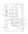
第1実施例の弾性表面波装置は、図1に模式的に示した電極構成の素子チップを備える。素子チップには、4つの弾性表面波フィルタ101〜104などが、例えば、40±5°YカットX伝搬LiTaO3基板上にAl電極により形成されている。弾性表面波フィルタ101〜104は、弾性表面波の伝搬方向に沿って配置された3つのIDTをそれぞれ含む縦結合共振子型フィルタである。 The surface acoustic wave device according to the first embodiment includes an element chip having an electrode configuration schematically shown in FIG. In the element chip, four surface acoustic wave filters 101 to 104 are formed by Al electrodes on, for example, a 40 ± 5 ° Y-cut X-propagation LiTaO 3 substrate. The surface acoustic wave filters 101 to 104 are longitudinally coupled resonator type filters each including three IDTs arranged along the propagation direction of the surface acoustic wave.
弾性表面波フィルタ101と102、弾性表面波フィルタ103と104は、それぞれ、縦続接続する。弾性表面波フィルタ101と103は、電気的に並列接続となるように、不平衡信号端子105と接続する。弾性表面波フィルタ102と104は、直列接続となるように、それぞれ、平衡信号端子106,107と接続する。弾性表面波フィルタ104は、他の3つの弾性表面波フィルタ101,102,103に対して、伝送位相特性が約180度異なるように構成されている。
The surface acoustic wave filters 101 and 102 and the surface acoustic wave filters 103 and 104 are connected in cascade. The surface acoustic wave filters 101 and 103 are connected to the
弾性表面波フィルタ101は、弾性表面波の伝搬方向に沿って配置された3つのIDT108,109,110及び2つのリフレクタ111,112を備える。IDT109の両側を挟み込むようにIDT108,110が形成され、さらにその両側を挟み込むようにリフレクタ111、112が形成されている。図1に符号113,114で示した箇所において、IDT108と109の間、およびIDT109と110の間の数本の電極指のピッチが、IDT108,109,110の他の部分よりも小さい。
The surface
弾性表面波フィルタ102,103は、弾性表面波フィルタ101と同様に構成されている。弾性表面波フィルタ104も略同様に構成されているが、他の弾性表面波フィルタ101,102,103に対して伝送位相を約180度異ならせるため、IDT115,117に対するIDT116の向きを反転させている。これにより、平衡−不平衡変換機能を有する。
The surface acoustic wave filters 102 and 103 are configured in the same manner as the surface
また、IDT109に対する伝送位相がIDT108と110で約180度異なるように構成されている。これにより、引き回し121,122を伝送する電気信号の位相は約180度異なるようになるが、IDT118,120のIDT119に対する伝送位相も約180°度異なるように構成されているので、IDT118,120からIDT119に伝搬する表面波の位相は等しくなる。弾性表面波フィルタ103,104についても、同様に構成されている。このように構成することで、弾性表面波装置の平衡度が向上する。
Further, the transmission phase with respect to the IDT 109 is configured to be different by about 180 degrees between the
図6は、第1実施例の弾性表面波装置のパッケージの裏面を、上面から見た透視図である。図1との関係では、端子201が端子105に接続される不平衡信号端子、端子202,203がそれぞれ端子106,107に接続される平衡信号端子、端子204,205,206がアース端子である。
FIG. 6 is a perspective view of the back surface of the surface acoustic wave device according to the first embodiment as viewed from above. In relation to FIG. 1,
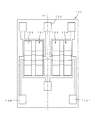
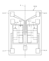
図9は、素子チップの圧電基板100上のレイアウトを示す。図8に示した構成とは異なり、各弾性表面波フィルタ101〜104は、弾性表面波の伝搬方向が長方形の圧電基板100の長辺と平行な方向となるように、配置する。さらに、弾性表面波フィルタ101〜104は、弾性表面波の伝搬方向に対して垂直方向、すなわち、圧電基板100の短辺に平行な方向に並べる。平衡信号端子106,107をはじめとする圧電基板100上のレイアウトは、圧電基板100の長辺に平行な方向に延在する長手方向の中心線Aに関して対称となっている。
FIG. 9 shows a layout of the element chip on the
第1実施例の弾性表面波装置は、図10に示すように、圧電基板100の電極面とパッケージ300のダイアタッチ面303の間をバンプ306で接続するフェイスダウン工法を用いて作製されている。パッケージ300は、底板301と側壁部302、キャップ304からなっている。
As shown in FIG. 10, the surface acoustic wave device according to the first embodiment is manufactured by using a face-down method in which the electrode surface of the
次に、詳細な設計例を説明する。 Next, a detailed design example will be described.
弾性表面波フィルタ101の設計諸元の一例は、ピッチを小さくしていない電極指のピッチで決まる波長をλIとすると、以下のようになる。
交叉幅:22.3λI
IDT本数(108,109,110の順):(4)25/(4)32(4)/25(4)本(カッコ内はピッチを小さくした電極指の本数)
リフレクタ本数:70本
デューティ:0.72(IDT)、0.55(リフレクタ)
電極膜厚:0.085λI
An example of the design specifications of the surface
Cross width: 22.3λ I
Number of IDTs (in order of 108, 109, 110): (4) 25 / (4) 32 (4) / 25 (4) (number of electrode fingers with a smaller pitch in parentheses)
Number of reflectors: 70 Duty: 0.72 (IDT), 0.55 (reflector)
Electrode film thickness: 0.085λ I
弾性表面波フィルタ102,103,104の設計諸元も、弾性表面波フィルタ101と同じである。ただし、前述したように、弾性表面波フィルタ104は、伝送位相が約180度異なるように、IDT115,117に対するIDT116の向きを反転している。
The design specifications of the surface acoustic wave filters 102, 103, and 104 are the same as those of the surface
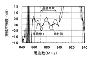
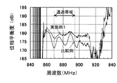
上記設計諸元の弾性表面波装置(実施例1)について、図11に振幅平衡度、図12に位相平衡度、図13に挿入損失を示す。比較のため、図8の構成(比較例)の場合の各特性も、合わせて示す。比較例は、圧電基板上のレイアウトが実施例1と異なる以外は、弾性表面波フィルタの設計諸元やパッケージは同じである。 FIG. 11 shows the amplitude balance, FIG. 12 shows the phase balance, and FIG. 13 shows the insertion loss for the surface acoustic wave device (Example 1) having the above-mentioned design specifications. For comparison, each characteristic in the case of the configuration of FIG. 8 (comparative example) is also shown. In the comparative example, the design specifications and package of the surface acoustic wave filter are the same except that the layout on the piezoelectric substrate is different from that in the first embodiment.
図11から、ADC受信用フィルタの通過帯域869〜894MHzにおいて、振幅平衡度は、比較例では−0.5〜+0.6dB(偏差1.1dB、偏差が小さいほど良い)であるのに対し、実施例1では−0.2〜+0.3dB(偏差0.5dB)であり、約0.6dB振幅平衡度が改善されていることが分かる。 From FIG. 11, in the pass band 869 to 894 MHz of the ADC reception filter, the amplitude balance is −0.5 to +0.6 dB (deviation 1.1 dB, the smaller the deviation is better) in the comparative example, In Example 1, it is -0.2- + 0.3 dB (deviation 0.5 dB), and it turns out that about 0.6 dB amplitude balance is improved.
図12から、位相平衡度は、比較例では180度に対して−8〜0度(偏差8度、偏差が小さいほど良い)であるのに対し、実施例1では−3〜+1度(偏差4度)であり、約4度位相平衡度が改善されていることが分かる。
From FIG. 12, the phase balance is −8 to 0 degrees with respect to 180 degrees in the comparative example (
図13から、比較例に対して実施例1は、通過帯域外の減衰量が、5〜15dB程度改善されていることが分かる。 From FIG. 13, it can be seen that the attenuation amount outside the passband is improved by about 5 to 15 dB in the first embodiment compared to the comparative example.
このように弾性表面波装置の平衡信号端子間の平衡度が改善しているのは、圧電基板100の長辺と平行な方向を弾性表面波の伝搬方向とし、さらに弾性表面波フィルタ101〜104を弾性表面波の伝搬方向に垂直方向に並べたことで、圧電基板上のレイアウトをほぼ左右対称としたことによる効果である。
In this way, the balance between the balanced signal terminals of the surface acoustic wave device is improved because the direction parallel to the long side of the
次に、第1実施例の変形例について、さらに説明する。 Next, a modification of the first embodiment will be further described.
パッケージの裏面端子レイアウトは、図6の6端子とする代わりに、図9の圧電基板上のレイアウトにそのまま対応して、図7のように5端子のレイアウトとしても、良好な平衡信号端子間の平衡度を実現することができる。 The rear surface terminal layout of the package corresponds to the layout on the piezoelectric substrate of FIG. 9 as it is instead of the 6 terminals of FIG. 6, and the layout of 5 terminals as shown in FIG. A degree of balance can be realized.
パッケージと素子チップとを接続する方法は、図10に示したフェイスダウン工法に限らず、例えばワイヤボンド工法であってもよい。 The method of connecting the package and the element chip is not limited to the face-down method shown in FIG. 10, and may be a wire bond method, for example.
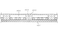
素子チップを封止する構成は、図10のように素子チップをパッケージに収納しキャップで覆う構成に限らない。例えば図14のように、集合基板401上に素子チップ402をフリップチップ工法で接合し、その上を樹脂403で覆って封止した後、ダイシングにより切断線404に沿って1パッケージ単位に切断するようにしてもよい。あるいは図15のように、同じく集合基板501上に素子チップ502をフリップチップ工法で接合し、その上をシート状の樹脂材503で覆って封止した後、ダイシングにより切断線504に沿って1パッケージ単位に切断するようにしてもよい。
The configuration for sealing the element chip is not limited to the configuration in which the element chip is housed in a package and covered with a cap as shown in FIG. For example, as shown in FIG. 14, the element chip 402 is bonded onto the
弾性表面波フィルタ101〜104の設計諸元は、すべて同じとすることは必須ではなく、リフレクタの本数を異ならせてもよい。例えば図16のように、弾性表面波フィルタ101a,103aと、102a,104aとで、リフレクタの本数が異なり、中心線Aに関して対称なレイアウトとしてもよい。図17のように、中心線Aの両側で弾性表面波フィルタ101b〜104bのリフレクタの本数が異なり、中心線Aに関する対称性が完全ではないが、略対称であるレイアウトとしてもよい。また、必要に応じて、リフレクタの本数以外の設計パラメータを異ならせてもよい。 The design specifications of the surface acoustic wave filters 101 to 104 are not necessarily the same, and the number of reflectors may be different. For example, as shown in FIG. 16, the surface acoustic wave filters 101a, 103a and 102a, 104a have different numbers of reflectors and may have a symmetric layout with respect to the center line A. As shown in FIG. 17, the number of reflectors of the surface acoustic wave filters 101b to 104b is different on both sides of the center line A, and the symmetry with respect to the center line A is not perfect, but a layout that is substantially symmetric may be used. Moreover, you may vary design parameters other than the number of reflectors as needed.
また、すべての弾性表面波フィルタ101〜104を、まっすぐ一列に揃えて配置する代わりに、例えば図18のように、圧電基板100cの大きさがほぼ変わらず、さらに中心線Aに対してほぼ左右対称を保てる程度に、弾性表面波フィルタ101c〜104cを圧電基板10cの長辺と平行にずらしてもよい。 Further, instead of arranging all the surface acoustic wave filters 101 to 104 in a straight line, the size of the piezoelectric substrate 100c is not substantially changed as shown in FIG. The surface acoustic wave filters 101c to 104c may be shifted in parallel with the long side of the piezoelectric substrate 10c so that the symmetry can be maintained.
基板は、40±5°YカットX伝搬LiTaO3に限らず、64〜72°YカットX伝搬LiNbO3、41°YカットX伝搬LiNbO3など、他のものでも同様な効果が得られる。 The substrate is not limited to 40 ± 5 ° Y-cut X-propagating LiTaO 3 , but the same effect can be obtained by using other substrates such as 64-72 ° Y-cut X-propagating LiNbO 3 and 41 ° Y-cut X-propagating LiNbO 3 .
次に、第2実施例の弾性表面波装置について、図6、図19及び図20を参照しながら説明する。 Next, a surface acoustic wave device according to a second embodiment will be described with reference to FIGS.
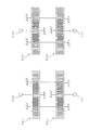
第2実施例は、4つの弾性表面波フィルタ501〜504を用いて、平衡信号入力−平衡信号出力のフィルタ(以下、「平衡−平衡フィルタ」という。)を構成している。 In the second embodiment, four surface acoustic wave filters 501 to 504 are used to constitute a balanced signal input-balanced signal output filter (hereinafter referred to as "balanced-balanced filter").
図19に、素子構成を示す。弾性表面波フィルタ501と502、弾性表面波フィルタ503と504は、それぞれ、縦続接続する。弾性表面波フィルタ501,503は、それぞれ、平衡信号端子505,506に直列に接続する。弾性表面波フィルタ502,504は、それぞれ、平衡信号端子507,508に直列に接続する。
FIG. 19 shows an element configuration. The surface acoustic wave filters 501 and 502 and the surface acoustic wave filters 503 and 504 are connected in cascade. The surface acoustic wave filters 501 and 503 are connected in series to
図20は、圧電基板500上のレイアウトを示す。第2実施例と同様に、長方形の圧電基板500の長辺と平行な方向を弾性表面波の伝搬方向とし、さらに弾性表面波フィルタ501〜504を弾性表面波の伝搬方向に垂直に(すなわち、圧電基板500の短辺と平行な方向に)並べている。また、長手方向の中心線Aに対して、平衡信号端子505と506、507と508をはじめとする圧電基板上のレイアウトが、ほぼ左右対称になるように構成する。
FIG. 20 shows a layout on the piezoelectric substrate 500. As in the second embodiment, the direction parallel to the long side of the rectangular piezoelectric substrate 500 is the surface acoustic wave propagation direction, and the surface acoustic wave filters 501 to 504 are perpendicular to the surface acoustic wave propagation direction (ie, They are arranged in a direction parallel to the short side of the piezoelectric substrate 500. Further, the layout on the piezoelectric substrate including the
第2実施例のパッケージは、図6の裏面端子レイアウトを有する。図20との関係において、平衡信号端子505,506はそれぞれ端子201,205と接続され、平衡信号端子507,508は端子202,203とそれぞれ接続される。端子204,206は、アース端子となる。
The package of the second embodiment has the back terminal layout of FIG. In relation to FIG. 20, the
第2実施例においても、圧電基板500上のレイアウトがほぼ左右対称になるように構成したので、平衡信号端子505と506、および507と508の間の平衡度が良好な、平衡−平衡フィルタが得られる。
Also in the second embodiment, since the layout on the piezoelectric substrate 500 is substantially symmetrical, a balanced-balanced filter having a good balance between the
次に、第3実施例について、図21〜図24を参照しながら、説明する。 Next, a third embodiment will be described with reference to FIGS.
図21及び図22に示すように、第3実施例は、縦結合共振子型の2つの弾性表面波フィルタ701,702と、1つのIDTをそれぞれ有する2つの弾性表面波共振子703、704とを用いて、平衡−不平衡変換機能を有する弾性表面波装置を構成した例である。
As shown in FIGS. 21 and 22, the third embodiment includes two longitudinally coupled resonator type surface acoustic wave filters 701 and 702, and two surface
図21に、素子構成を示す。弾性表面波フィルタ701に弾性表面波共振子703、弾性表面波フィルタ702に弾性表面波共振子704を、それぞれ直列接続する。弾性表面波フィルタ701と702の一方の端子は、電気的に並列接続となるように、不平衡信号端子705に接続する。弾性表面波共振子703、704は、電気的に直列接続となるように、それぞれ、平衡信号端子706,707に接続する。
FIG. 21 shows an element configuration. A surface
図22に、圧電基板700上のレイアウトを示す。第1及び第2実施例と同様に、長方形の圧電基板700の長辺と平行な方向を弾性表面波の伝搬方向とする。弾性表面波フィルタ701,702および弾性表面波共振子703,704は、弾性表面波の伝搬方向に対して垂直に、すなわち圧電基板700の短辺と平行な方向に、配置する。また、平衡信号端子706と707をはじめとする圧電基板上のレイアウトは、圧電基板700の長手方向の中心線Aに対してほぼ左右対称になる。
FIG. 22 shows a layout on the
第3実施例においても、パッケージは図6の裏面端子レイアウトを有する。図22との関係では、不平衡信号端子705は端子201、平衡信号端子706,707はそれぞれ端子202,203と接続される。端子204,205,206は、アース端子となる。なお、図7の裏面端子レイアウトを有するパッケージを用いてもよい。
Also in the third embodiment, the package has the back terminal layout of FIG. In relation to FIG. 22, the
第3実施例においても、圧電基板700上のレイアウトがほぼ左右対称になるように構成したので、平衡信号端子706と707の間の平衡度が良好な、平衡−不平衡変換機能を有する弾性表面波装置が得られる。
Also in the third embodiment, since the layout on the
次に、第3実施例の変形例について説明する。 Next, a modification of the third embodiment will be described.
弾性表面波共振子703,704を平衡信号端子706,707に直列に接続する構成に代え、例えば、図23のように、弾性表面波フィルタ701,702を平行信号端子706,707にそれぞれ接続し、弾性表面波共振子703,704を不平衡信号端子705に接続してもよい。また、図24のように、弾性表面波共振子703,704及び703',704'を両方の端子705及び706,707に接続する場合においても、圧電基板700の長手方向の中心線Aに対してほぼ左右対称にレイアウトすることで、平衡度が良好な平衡−不平衡変換機能を有する弾性表面波装置が得られる。
Instead of connecting the surface
次に、第4実施例の弾性表面波装置について、図25及び図26を参照しながら説明する。第4実施例は、弾性表面波フィルタ801,802と弾性表面波共振子803,804を用いて、平衡−平衡フィルタを構成した例である。
Next, a surface acoustic wave device according to a fourth embodiment will be described with reference to FIGS. The fourth embodiment is an example in which a balanced-balance filter is configured by using surface acoustic wave filters 801 and 802 and surface
図25に、素子構成を示す。弾性表面波フィルタ801と弾性表面波共振子803、弾性表面波フィルタ802と弾性表面波共振子804は、それぞれ、直列に接続する。弾性表面波フィルタ801と802は、電気的に直列接続となるように、平衡信号端子805,806にそれぞれ接続する。弾性表面波共振子803,804の一方の端子は、電気的に直列接続となるように、それぞれ、平衡信号端子807,808に接続する。
FIG. 25 shows the element structure. The surface
図26に、圧電基板800上のレイアウトを示す。第1乃至第3実施例と同様に、長方形の圧電基板800の長辺と平行な方向を弾性表面波の伝搬方向とする。弾性表面波フィルタ801,802および弾性表面波共振子803,804は、弾性表面波の伝搬方向に対して垂直方向、すなわち圧電基板800と短辺と平行な方向に並べる。また、平衡信号端子805と806、807と808をはじめとする圧電基板800上のレイアウトは、圧電基板800の長手方向の中心線Aに関してほぼ左右対称になるように構成されている。
FIG. 26 shows a layout on the
第4実施例のパッケージは、図6の裏面端子レイアウトを有する。図26との関係では、平衡信号端子805,806はそれぞれ端子201,205と接続され、平衡信号端子807,808はそれぞれ端子202,203と接続される。端子204,206は、アース端子となる。
The package of the fourth embodiment has the back terminal layout of FIG. In relation to FIG. 26,
第4実施例においても、圧電基板800のレイアウトがほぼ左右対称になるように構成したので、平衡信号端子805と806、および807と808の間の平衡度が良好な、平衡−平衡フィルタが得られる。
Also in the fourth embodiment, since the layout of the
次に、第5実施例の弾性表面波装置について、図27及び図28を参照しながら説明する。 Next, a surface acoustic wave device according to a fifth embodiment will be described with reference to FIGS.
第5実施例は、第1乃至第4実施例の圧電基板のレイアウトを用いて、マルチバンド弾性表面波装置を構成した例である。 The fifth embodiment is an example in which a multiband surface acoustic wave device is configured using the layout of the piezoelectric substrate of the first to fourth embodiments.
図28のように、長方形の圧電基板600,601上のレイアウトが第1乃至第4実施例のいずれかである2つの素子チップを、圧電基板600,601の長辺同士が隣接するように並べて、パッケージに実装する。マルチバンド弾性表面波装置を構成する場合、図28のように圧電基板600,601の短辺と平行な方向に圧電基板600,601を配列する方が、弾性表面波装置の縦横比が大きくならず、有利である。 As shown in FIG. 28, two element chips whose layout on the rectangular piezoelectric substrates 600 and 601 is one of the first to fourth embodiments are arranged so that the long sides of the piezoelectric substrates 600 and 601 are adjacent to each other. Implement it in the package. When a multiband surface acoustic wave device is configured, the aspect ratio of the surface acoustic wave device is larger when the piezoelectric substrates 600 and 601 are arranged in a direction parallel to the short sides of the piezoelectric substrates 600 and 601 as shown in FIG. It is advantageous.
図27は、パッケージ裏面端子の一例である。端子901または902を一方の素子チップの不平衡信号端子(または901,902両方を平衡信号端子とする)、903または904を他方の素子チップの不平衡信号端子(または903,904両方を平衡信号端子とする)、905,906を一方の素子チップの平衡信号端子、907,908を他方の素子チップの平衡信号端子とし、残りの端子をアース端子とする。
FIG. 27 is an example of a package back surface terminal.
第5実施例において、第1乃至第4実施例の圧電基板のレイアウトを用いることで、平衡信号端子間の平衡度が優れた、マルチバンド弾性表面波装置が得られる。 In the fifth embodiment, a multiband surface acoustic wave device with excellent balance between balanced signal terminals can be obtained by using the layout of the piezoelectric substrate of the first to fourth embodiments.
次に、第5実施例の変形例について説明する。 Next, a modification of the fifth embodiment will be described.
1つのパッケージに3つ以上の素子チップを実装してもよい。例えば図29のように、端子1001または1002を第1の素子チップの不平衡信号端子(または1001,1002両方を平衡信号端子とする)、1003または1004を第2の素子チップの不平衡信号端子(または1003,1004両方を平衡信号端子とする)、1005または1006を第3の素子チップの不平衡信号端子(または1005、1006両方を平衡信号端子とする)、1007,1008を第1の素子チップの平衡信号端子、1009,1010を第2の素子チップの平衡信号端子、1011,1012を第3の素子チップの平衡信号端子とし、残りの端子をアース端子として、3つの素子チップを1つのパッケージに実装してもよい。それ以上の数の素子チップを1つのパッケージに実装する場合も、第1乃至第4実施例の圧電基板上のレイアウトを有する素子チップを用いることで、平衡信号端子間の平衡度が優れた、マルチバンド弾性表面波装置が得られる。 Three or more element chips may be mounted on one package. For example, as shown in FIG. 29, terminal 1001 or 1002 is the unbalanced signal terminal of the first element chip (or both 1001 and 1002 are balanced signal terminals), and 1003 or 1004 is the unbalanced signal terminal of the second element chip. (Or both 1003 and 1004 are balanced signal terminals), 1005 or 1006 is an unbalanced signal terminal of the third element chip (or both 1005 and 1006 are balanced signal terminals), and 1007 and 1008 are first elements. The balanced signal terminal of the chip, 1009 and 1010 are the balanced signal terminals of the second element chip, 1011 and 1012 are the balanced signal terminals of the third element chip, the remaining terminals are the ground terminals, and the three element chips are one It may be mounted on a package. Even when a larger number of element chips are mounted on one package, the balance between balanced signal terminals is excellent by using the element chips having the layout on the piezoelectric substrate of the first to fourth embodiments. A multiband surface acoustic wave device is obtained.
次に、第6実施例の通信機について、図30を参照しながら説明する。 Next, a communication device according to a sixth embodiment will be described with reference to FIG.
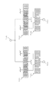
図30は、マルチバンド携帯電話など、異なる方式に対応した通信機160の要部ブロック図である。通信機160は、スイッチSWにより、受信周波数を切り替えることができるようになっている。 FIG. 30 is a principal block diagram of a communication device 160 that supports different systems, such as a multi-band mobile phone. The communication device 160 can switch the reception frequency by the switch SW.
アンテナ161に、デュプレクサ162が接続されている。デュプレクサ162には、スイッチSWを介して、2系統の受信回路が接続されている。すなわち、スイッチSWとIF段の弾性表面波フィルタ169,169aとの間には、受信側RF弾性表面波フィルタ164,164a、増幅器165,165a、及び受信側ミキサ163,163aが、それぞれ接続されている。また、デュプレクサ162と送信側のミキサ166との間には、RF段を構成する増幅器167及び送信側弾性表面波フィルタ168が接続されている。例えば、受信側RF弾性表面波フィルタ164,164aに、第1実施例や第5実施例の弾性表面波装置を用いれば、配線を短くして、通信機160の回路基板を小型化することができ、好適である。
A duplexer 162 is connected to the antenna 161. Two systems of receiving circuits are connected to the duplexer 162 via the switch SW. That is, receiving-side RF surface acoustic wave filters 164 and 164a,
なお、本発明の弾性表面波装置及び通信機は、上記実施例に限定されるものではなく、種々の態様で実施可能である。 The surface acoustic wave device and the communication device of the present invention are not limited to the above-described embodiments, and can be implemented in various modes.
100 圧電基板
101 弾性表面波フィルタ(第1の縦結合共振子型弾性表面波フィルタ)
102 弾性表面波フィルタ(第2の縦結合共振子型弾性表面波フィルタ)
103 弾性表面波フィルタ(第3の縦結合共振子型弾性表面波フィルタ)
104 弾性表面波フィルタ(第4の縦結合共振子型弾性表面波フィルタ)
105 不平衡信号端子(第1の端子)
106 平衡信号端子(第2の端子)
107 平衡信号端子(第3の端子)
108,109,110 IDT
118,119,120 IDT
201 端子(第1の外部端子)
202 端子(第2の外部端子)
203 端子(第3の外部端子)
204 端子(アース端子、第4の外部端子)
205 端子(アース端子)
206 端子(アース端子)
500 圧電基板
501 弾性表面波フィルタ(第1の縦結合共振子型弾性表面波フィルタ)
502 弾性表面波フィルタ(第2の縦結合共振子型弾性表面波フィルタ)
503 弾性表面波フィルタ(第3の縦結合共振子型弾性表面波フィルタ)
504 弾性表面波フィルタ(第4の縦結合共振子型弾性表面波フィルタ)
505 平衡信号端子(第1の端子)
506 平衡信号端子(第2の端子)
507 平衡信号端子(第3の端子)
508 平衡信号端子(第4の端子)
600,601 圧電基板
700 圧電基板
701 弾性表面波フィルタ(第1の縦結合共振子型弾性表面波フィルタ)
702 弾性表面波フィルタ(第2の縦結合共振子型弾性表面波フィルタ)
703 弾性表面波フィルタ(第1の弾性表面波共振子)
704 弾性表面波フィルタ(第2の弾性表面波共振子)
705 平衡信号端子(第1の端子)
706 平衡信号端子(第2の端子)
707 平衡信号端子(第3の端子)
800 圧電基板
801 弾性表面波フィルタ(第1の縦結合共振子型弾性表面波フィルタ)
802 弾性表面波フィルタ(第2の縦結合共振子型弾性表面波フィルタ)
803 弾性表面波共振子(第1の弾性表面波共振子)
804 弾性表面波共振子(第2の弾性表面波共振子)
805 平衡信号端子(第1の端子)
806 平衡信号端子(第2の端子)
807 平衡信号端子(第3の端子)
808 平衡信号端子(第4の端子)
100
102 surface acoustic wave filter (second longitudinally coupled resonator type surface acoustic wave filter)
103 surface acoustic wave filter (third longitudinally coupled resonator type surface acoustic wave filter)
104 surface acoustic wave filter (fourth longitudinally coupled resonator type surface acoustic wave filter)
105 Unbalanced signal terminal (first terminal)
106 Balance signal terminal (second terminal)
107 balanced signal terminal (third terminal)
108, 109, 110 IDT
118, 119, 120 IDT
201 terminal (first external terminal)
202 terminal (second external terminal)
203 terminal (third external terminal)
204 terminals (ground terminal, fourth external terminal)
205 terminal (ground terminal)
206 terminal (ground terminal)
500
502 surface acoustic wave filter (second longitudinally coupled resonator type surface acoustic wave filter)
503 SAW filter (third longitudinally coupled resonator type SAW filter)
504 surface acoustic wave filter (fourth longitudinally coupled resonator type surface acoustic wave filter)
505 Balance signal terminal (first terminal)
506 Balance signal terminal (second terminal)
507 Balanced signal terminal (third terminal)
508 Balance signal terminal (fourth terminal)
600, 601
702 surface acoustic wave filter (second longitudinally coupled resonator type surface acoustic wave filter)
703 surface acoustic wave filter (first surface acoustic wave resonator)
704 Surface acoustic wave filter (second surface acoustic wave resonator)
705 Balance signal terminal (first terminal)
706 Balance signal terminal (second terminal)
707 Balance signal terminal (third terminal)
800
802 surface acoustic wave filter (second longitudinally coupled resonator type surface acoustic wave filter)
803 surface acoustic wave resonator (first surface acoustic wave resonator)
804 surface acoustic wave resonator (second surface acoustic wave resonator)
805 Balance signal terminal (first terminal)
806 Balance signal terminal (second terminal)
807 Balance signal terminal (third terminal)
808 Balance signal terminal (fourth terminal)
Claims (9)
弾性表面波の伝搬方向に沿って配置された3つのIDTをそれぞれ有する第1乃至第4の縦結合共振子型弾性表面波フィルタと、
前記第1の縦結合共振子型弾性表面波フィルタの中央に配置された前記IDTの一端と、前記第3の縦結合共振子型弾性表面波フィルタの中央に配置された前記IDTの一端とに電気的に接続された第1の端子と、
前記第2の縦結合共振子型弾性表面波フィルタの中央に配置された前記IDTの一端に電気的に接続された第2の端子と、
前記第4の縦結合共振子型弾性表面波フィルタの中央に配置された前記IDTの一端に電気的に接続された第3の端子とが形成され、
前記第1の縦結合共振子型弾性表面波フィルタと前記第2の縦結合共振子型弾性表面波フィルタとが縦続接続され、
前記第3の縦結合共振子型弾性表面波フィルタと前記第4の縦結合共振子型弾性表面波フィルタとが縦続接続され、
前記第1乃至第4の縦結合共振子型弾性表面波フィルタのうち、1つの位相が他の3つの位相と180度異なる、素子チップを備えた弾性表面波装置であって、
前記第1乃至第4の縦結合共振子型弾性表面波フィルタは、それぞれの弾性表面波の伝搬方向が前記圧電基板の長辺と平行な方向となるように、前記圧電基板の短辺と平行な方向に並べて配置されたことを特徴とする、弾性表面波装置。 On a rectangular piezoelectric substrate,
First to fourth longitudinally coupled resonator type surface acoustic wave filters each having three IDTs arranged along the propagation direction of the surface acoustic wave;
One end of the IDT disposed at the center of the first longitudinally coupled resonator type surface acoustic wave filter and one end of the IDT disposed at the center of the third longitudinally coupled resonator type surface acoustic wave filter A first terminal electrically connected;
A second terminal electrically connected to one end of the IDT disposed in the center of the second longitudinally coupled resonator type surface acoustic wave filter;
A third terminal electrically connected to one end of the IDT disposed in the center of the fourth longitudinally coupled resonator type surface acoustic wave filter;
The first longitudinally coupled resonator type surface acoustic wave filter and the second longitudinally coupled resonator type surface acoustic wave filter are cascade-connected,
The third longitudinally coupled resonator type surface acoustic wave filter and the fourth longitudinally coupled resonator type surface acoustic wave filter are cascade-connected,
Of the first to fourth longitudinally coupled resonator type surface acoustic wave filters, a surface acoustic wave device including an element chip, wherein one phase is 180 degrees different from the other three phases,
The first to fourth longitudinally coupled resonator type surface acoustic wave filters are parallel to the short sides of the piezoelectric substrate so that the propagation directions of the respective surface acoustic waves are parallel to the long sides of the piezoelectric substrate. A surface acoustic wave device characterized by being arranged side by side in various directions.
弾性表面波の伝搬方向に沿って配置された3つのIDTをそれぞれ有する第1及び第2の縦結合共振子型弾性表面波フィルタと、
1つのIDTをそれぞれ有する第1及び第2の弾性表面波共振子と、
前記第1の縦結合共振子型弾性表面波フィルタの中央に配置された前記IDTの一端と、前記第2の縦結合共振子型弾性表面波フィルタの中央に配置された前記IDTの一端とに電気的に接続された第1の端子と、
前記第1の弾性表面波共振子の前記IDTの一端に電気的に接続された第2の端子と、
前記第2の弾性表面波共振子の前記IDTの一端に電気的に接続された第3の端子とが形成され、
前記第1の縦結合共振子型弾性表面波フィルタの両側に配置された前記IDTのそれぞれの一端が、前記第1の弾性表面波共振子の前記IDTの他端に接続され、
前記第2の縦結合共振子型弾性表面波フィルタの両側に配置された前記IDTのそれぞれの一端が、前記第2の弾性表面波共振子の前記IDTの他端に接続され、
前記第1及び第2の縦結合共振子型弾性表面波フィルタの位相が180度異なる、素子チップを備えた弾性表面波装置であって、
前記第1及び第2の縦結合共振子型弾性表面波フィルタと前記第1及び第2の弾性表面波共振子は、それぞれの弾性表面波の伝搬方向が前記圧電基板の長辺と平行な方向となるように、前記圧電基板の短辺と平行な方向に並べて配置されたことを特徴とする、弾性表面波装置。 On a rectangular piezoelectric substrate,
First and second longitudinally coupled resonator type surface acoustic wave filters each having three IDTs arranged along the propagation direction of the surface acoustic wave;
First and second surface acoustic wave resonators each having one IDT;
One end of the IDT disposed at the center of the first longitudinally coupled resonator type surface acoustic wave filter and one end of the IDT disposed at the center of the second longitudinally coupled resonator type surface acoustic wave filter A first terminal electrically connected;
A second terminal electrically connected to one end of the IDT of the first surface acoustic wave resonator;
A third terminal electrically connected to one end of the IDT of the second surface acoustic wave resonator;
One end of each of the IDTs disposed on both sides of the first longitudinally coupled resonator type surface acoustic wave filter is connected to the other end of the IDT of the first surface acoustic wave resonator,
One end of each of the IDTs disposed on both sides of the second longitudinally coupled resonator type surface acoustic wave filter is connected to the other end of the IDT of the second surface acoustic wave resonator,
A surface acoustic wave device including an element chip, wherein the phases of the first and second longitudinally coupled resonator type surface acoustic wave filters are different by 180 degrees,
The first and second longitudinally coupled resonator type surface acoustic wave filters and the first and second surface acoustic wave resonators have directions in which the propagation directions of the respective surface acoustic waves are parallel to the long sides of the piezoelectric substrate. The surface acoustic wave device is arranged side by side in a direction parallel to the short side of the piezoelectric substrate.
弾性表面波の伝搬方向に沿って配置された3つのIDTをそれぞれ有する第1乃至第4の縦結合共振子型弾性表面波フィルタと、
前記第1の縦結合共振子型弾性表面波フィルタの中央に配置された前記IDTの一端に電気的に接続された第1の端子と、
前記第3の縦結合共振子型弾性表面波フィルタの中央に配置された前記IDTの一端に電気的に接続された第2の端子と、
前記第2の縦結合共振子型弾性表面波フィルタの中央に配置された前記IDTの一端に電気的に接続された第3の端子と、
前記第4の縦結合共振子型弾性表面波フィルタの中央に配置された前記IDTの一端に電気的に接続された第4の端子とが形成され、
前記第1の縦結合共振子型弾性表面波フィルタと前記第2の縦結合共振子型弾性表面波フィルタとが縦続接続され、
前記第3の縦結合共振子型弾性表面波フィルタと前記第4の縦結合共振子型弾性表面波フィルタとが縦続接続され、
前記第1乃至第4の縦結合共振子型弾性表面波フィルタは、それぞれの弾性表面波の伝搬方向が前記圧電基板の長辺と平行な方向となるように、前記圧電基板の短辺と平行な方向に並べて配置されたことを特徴とする、弾性表面波装置。 On a rectangular piezoelectric substrate,
First to fourth longitudinally coupled resonator type surface acoustic wave filters each having three IDTs arranged along the propagation direction of the surface acoustic wave;
A first terminal electrically connected to one end of the IDT disposed in the center of the first longitudinally coupled resonator type surface acoustic wave filter;
A second terminal electrically connected to one end of the IDT disposed in the center of the third longitudinally coupled resonator type surface acoustic wave filter;
A third terminal electrically connected to one end of the IDT disposed in the center of the second longitudinally coupled resonator type surface acoustic wave filter;
A fourth terminal electrically connected to one end of the IDT disposed in the center of the fourth longitudinally coupled resonator type surface acoustic wave filter;
The first longitudinally coupled resonator type surface acoustic wave filter and the second longitudinally coupled resonator type surface acoustic wave filter are cascade-connected,
The third longitudinally coupled resonator type surface acoustic wave filter and the fourth longitudinally coupled resonator type surface acoustic wave filter are cascade-connected,
The first to fourth longitudinally coupled resonator type surface acoustic wave filters are parallel to the short sides of the piezoelectric substrate so that the propagation directions of the respective surface acoustic waves are parallel to the long sides of the piezoelectric substrate. A surface acoustic wave device characterized by being arranged side by side in various directions.
弾性表面波の伝搬方向に沿って配置された3つのIDTをそれぞれ有する第1及び第2の縦結合共振子型弾性表面波フィルタと、
1つのIDTをそれぞれ有する第1及び第2の弾性表面波共振子と、
前記第1の縦結合共振子型弾性表面波フィルタの中央に配置された前記IDTの一端に電気的に接続された第1の端子と、
前記第2の縦結合共振子型弾性表面波フィルタの中央に配置された前記IDTの一端に電気的に接続された第2の端子と、
前記第1の弾性表面波共振子の前記IDTの一端に電気的に接続された第3の端子と、
前記第2の弾性表面波共振子の前記IDTの一端に電気的に接続された第4の端子とが形成され、
前記第1の縦結合共振子型弾性表面波フィルタの両側に配置された前記IDTのそれぞれの一端が、前記第1の弾性表面波共振子の前記IDTの他端に接続され、
前記第2の縦結合共振子型弾性表面波フィルタの両側に配置された前記IDTのそれぞれの一端が、前記第2の弾性表面波共振子の前記IDTの他端に接続され、
前記第1及び第2の縦結合共振子型弾性表面波フィルタと前記第1及び第2の弾性表面波共振子は、それぞれの弾性表面波の伝搬方向が前記圧電基板の長辺と平行な方向となるように、前記圧電基板の短辺と平行な方向に並べて配置されたことを特徴とする、弾性表面波装置。 On a rectangular piezoelectric substrate,
First and second longitudinally coupled resonator type surface acoustic wave filters each having three IDTs arranged along the propagation direction of the surface acoustic wave;
First and second surface acoustic wave resonators each having one IDT;
A first terminal electrically connected to one end of the IDT disposed in the center of the first longitudinally coupled resonator type surface acoustic wave filter;
A second terminal electrically connected to one end of the IDT disposed in the center of the second longitudinally coupled resonator type surface acoustic wave filter;
A third terminal electrically connected to one end of the IDT of the first surface acoustic wave resonator;
A fourth terminal electrically connected to one end of the IDT of the second surface acoustic wave resonator;
One end of each of the IDTs disposed on both sides of the first longitudinally coupled resonator type surface acoustic wave filter is connected to the other end of the IDT of the first surface acoustic wave resonator,
One end of each of the IDTs disposed on both sides of the second longitudinally coupled resonator type surface acoustic wave filter is connected to the other end of the IDT of the second surface acoustic wave resonator,
The first and second longitudinally coupled resonator type surface acoustic wave filters and the first and second surface acoustic wave resonators have directions in which the propagation directions of the respective surface acoustic waves are parallel to the long sides of the piezoelectric substrate. The surface acoustic wave device is arranged side by side in a direction parallel to the short side of the piezoelectric substrate.
Priority Applications (1)
| Application Number | Priority Date | Filing Date | Title |
|---|---|---|---|
| JP2004102471A JP4403861B2 (en) | 2004-03-31 | 2004-03-31 | Surface acoustic wave device |
Applications Claiming Priority (1)
| Application Number | Priority Date | Filing Date | Title |
|---|---|---|---|
| JP2004102471A JP4403861B2 (en) | 2004-03-31 | 2004-03-31 | Surface acoustic wave device |
Publications (2)
| Publication Number | Publication Date |
|---|---|
| JP2005294891A true JP2005294891A (en) | 2005-10-20 |
| JP4403861B2 JP4403861B2 (en) | 2010-01-27 |
Family
ID=35327396
Family Applications (1)
| Application Number | Title | Priority Date | Filing Date |
|---|---|---|---|
| JP2004102471A Expired - Fee Related JP4403861B2 (en) | 2004-03-31 | 2004-03-31 | Surface acoustic wave device |
Country Status (1)
| Country | Link |
|---|---|
| JP (1) | JP4403861B2 (en) |
Cited By (5)
| Publication number | Priority date | Publication date | Assignee | Title |
|---|---|---|---|---|
| JP2007142654A (en) * | 2005-11-16 | 2007-06-07 | Kyocera Corp | Surface acoustic wave device |
| WO2011077773A1 (en) * | 2009-12-25 | 2011-06-30 | 株式会社村田製作所 | Branching filter |
| WO2011092876A1 (en) * | 2010-01-28 | 2011-08-04 | 株式会社村田製作所 | Branching filter |
| US8912866B2 (en) | 2010-06-11 | 2014-12-16 | Murata Manufacturing Co., Ltd. | Dual-band surface acoustic wave filter and composite high-frequency component |
| US9912318B2 (en) | 2013-06-13 | 2018-03-06 | Murata Manufacturing Co., Ltd. | Filter device and duplexer |
-
2004
- 2004-03-31 JP JP2004102471A patent/JP4403861B2/en not_active Expired - Fee Related
Cited By (8)
| Publication number | Priority date | Publication date | Assignee | Title |
|---|---|---|---|---|
| JP2007142654A (en) * | 2005-11-16 | 2007-06-07 | Kyocera Corp | Surface acoustic wave device |
| WO2011077773A1 (en) * | 2009-12-25 | 2011-06-30 | 株式会社村田製作所 | Branching filter |
| US8416036B2 (en) | 2009-12-25 | 2013-04-09 | Murata Manufacturing Co., Ltd. | Branching filter |
| WO2011092876A1 (en) * | 2010-01-28 | 2011-08-04 | 株式会社村田製作所 | Branching filter |
| JP5168360B2 (en) * | 2010-01-28 | 2013-03-21 | 株式会社村田製作所 | Duplexer |
| US8791774B2 (en) | 2010-01-28 | 2014-07-29 | Murata Manufacturing Co., Ltd. | Branching filter |
| US8912866B2 (en) | 2010-06-11 | 2014-12-16 | Murata Manufacturing Co., Ltd. | Dual-band surface acoustic wave filter and composite high-frequency component |
| US9912318B2 (en) | 2013-06-13 | 2018-03-06 | Murata Manufacturing Co., Ltd. | Filter device and duplexer |
Also Published As
| Publication number | Publication date |
|---|---|
| JP4403861B2 (en) | 2010-01-27 |
Similar Documents
| Publication | Publication Date | Title |
|---|---|---|
| US7902940B2 (en) | Duplexer | |
| JP3931767B2 (en) | Surface acoustic wave device, communication device | |
| CN101682312B (en) | elastic wave splitter | |
| US7190242B2 (en) | Surface acoustic wave filter and communication unit | |
| US7459997B2 (en) | Elastic wave filter device and duplexer | |
| JP3918698B2 (en) | Surface acoustic wave device, communication device | |
| US7116189B2 (en) | Surface acoustic wave device and communication apparatus including the same | |
| US7902716B2 (en) | Surface acoustic wave device and communication apparatus | |
| US6756867B2 (en) | Surface acoustic wave filter and communication apparatus | |
| CN102804601B (en) | Elastic wave device and duplexer | |
| JP2003124777A (en) | Surface acoustic wave device | |
| US6597262B2 (en) | Surface acoustic wave filter and communication apparatus incorporating the same | |
| CN100417019C (en) | surface acoustic wave device | |
| JP4412326B2 (en) | Balanced SAW filter | |
| JP4403861B2 (en) | Surface acoustic wave device | |
| WO2011092876A1 (en) | Branching filter | |
| JP4063273B2 (en) | Surface acoustic wave device | |
| JP4329557B2 (en) | Surface acoustic wave device, communication device | |
| CN100512000C (en) | Balanced SAW filter | |
| WO2011065048A1 (en) | Acoustic wave filter and branching filter |
Legal Events
| Date | Code | Title | Description |
|---|---|---|---|
| A621 | Written request for application examination |
Free format text: JAPANESE INTERMEDIATE CODE: A621 Effective date: 20061213 |
|
| A977 | Report on retrieval |
Free format text: JAPANESE INTERMEDIATE CODE: A971007 Effective date: 20090708 |
|
| A131 | Notification of reasons for refusal |
Free format text: JAPANESE INTERMEDIATE CODE: A131 Effective date: 20090717 |
|
| A521 | Request for written amendment filed |
Free format text: JAPANESE INTERMEDIATE CODE: A523 Effective date: 20090901 |
|
| TRDD | Decision of grant or rejection written | ||
| A01 | Written decision to grant a patent or to grant a registration (utility model) |
Free format text: JAPANESE INTERMEDIATE CODE: A01 Effective date: 20091013 |
|
| A01 | Written decision to grant a patent or to grant a registration (utility model) |
Free format text: JAPANESE INTERMEDIATE CODE: A01 |
|
| A61 | First payment of annual fees (during grant procedure) |
Free format text: JAPANESE INTERMEDIATE CODE: A61 Effective date: 20091026 |
|
| FPAY | Renewal fee payment (event date is renewal date of database) |
Free format text: PAYMENT UNTIL: 20121113 Year of fee payment: 3 |
|
| R150 | Certificate of patent or registration of utility model |
Ref document number: 4403861 Country of ref document: JP Free format text: JAPANESE INTERMEDIATE CODE: R150 |
|
| FPAY | Renewal fee payment (event date is renewal date of database) |
Free format text: PAYMENT UNTIL: 20121113 Year of fee payment: 3 |
|
| FPAY | Renewal fee payment (event date is renewal date of database) |
Free format text: PAYMENT UNTIL: 20131113 Year of fee payment: 4 |
|
| LAPS | Cancellation because of no payment of annual fees |