JP2005294883A - Radio antenna - Google Patents
Radio antenna Download PDFInfo
- Publication number
- JP2005294883A JP2005294883A JP2004102412A JP2004102412A JP2005294883A JP 2005294883 A JP2005294883 A JP 2005294883A JP 2004102412 A JP2004102412 A JP 2004102412A JP 2004102412 A JP2004102412 A JP 2004102412A JP 2005294883 A JP2005294883 A JP 2005294883A
- Authority
- JP
- Japan
- Prior art keywords
- substrate
- wireless
- antenna
- radio
- wireless antenna
- Prior art date
- Legal status (The legal status is an assumption and is not a legal conclusion. Google has not performed a legal analysis and makes no representation as to the accuracy of the status listed.)
- Pending
Links
- 239000000758 substrate Substances 0.000 claims abstract description 65
- 239000004020 conductor Substances 0.000 claims abstract description 33
- 230000005855 radiation Effects 0.000 claims abstract description 7
- 230000005540 biological transmission Effects 0.000 claims abstract description 5
- 230000002093 peripheral effect Effects 0.000 claims description 7
- 230000004048 modification Effects 0.000 description 11
- 238000012986 modification Methods 0.000 description 11
- 230000010354 integration Effects 0.000 description 2
- 238000004519 manufacturing process Methods 0.000 description 2
- -1 polytetrafluoroethylene Polymers 0.000 description 2
- 229920001343 polytetrafluoroethylene Polymers 0.000 description 2
- 239000004810 polytetrafluoroethylene Substances 0.000 description 2
- 238000000034 method Methods 0.000 description 1
- 230000035515 penetration Effects 0.000 description 1
- 238000009751 slip forming Methods 0.000 description 1
Images
Landscapes
- Waveguide Aerials (AREA)
Abstract
Description
本発明は、無線アンテナに関し、特に誘電体導波路構造を有する無線アンテナに関する。 The present invention relates to a radio antenna, and more particularly to a radio antenna having a dielectric waveguide structure.
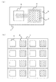
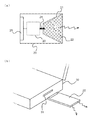
従来、無線モジュールからの電波を送受信する無線アンテナとして、例えば図1に示すような内部に導波路構造を有する無線アンテナ基板1が用いられてきた。代表的な無線アンテナ基板1には、平面基板の上面又は下面のいずれかに平面アンテナ2が設けられている。平面基板の内部には、壁構造体3によって囲まれた領域に導波路4が形成されており、平面アンテナ2はこの導波路4の領域内に配置される。このような構成によって、例えば平面アンテナ2で受信した電波は、導波路4内のみで伝達されることになる。そこで、無線アンテナ基板1に無線モジュール5を載置して無線モジュール5と導波路4とを例えば同軸ケーブル等の伝送路で接続すると、無線アンテナ基板1は、無線モジュールに対する送受信アンテナとしてだけでなく、無線モジュール5の固定基板としても機能することができる。
Conventionally, for example, a wireless antenna substrate 1 having a waveguide structure as shown in FIG. 1 has been used as a wireless antenna for transmitting and receiving radio waves from a wireless module. A typical wireless antenna substrate 1 is provided with a
また、現在では、図1(b)に示すように、例えばレーダシステム等に同一の無線モジュール5を複数アレイ化して用いる場合がある。このとき、図1(a)に示すような無線アンテナ基板1を用いれば、規則的に同一形状の安定したアレイ構造を構築することが可能となる。
Further, at present, as shown in FIG. 1B, for example, a plurality of the same
しかしながら、図1(a)に示すような従来の無線アンテナ基板1をアレイ化した場合、平面アンテナ2が設けられたアンテナ面側には無線モジュール5のための配置領域が合わせて必要となるため、集積度が低下してしまうという問題点があった。また、図1(b)のような集積度の低下を改善する方法として、平面アンテナ2を設ける面の裏面に無線モジュール5を設けることが考えられるが、この場合、通常はアンテナ面が取り付ける装置の外側を向くために無線モジュール5が取り付け面側に配置されることとなり、無線モジュール5の取り外しや調整が困難になってしまうという問題があった。
However, when the conventional wireless antenna substrate 1 as shown in FIG. 1A is arrayed, an arrangement area for the
そこで本発明は、上記のような問題を鑑み、無線モジュールを搭載しても全体の面積を小さくすることができる無線アンテナを提供することを目的とする。 In view of the above problems, an object of the present invention is to provide a wireless antenna that can reduce the entire area even when a wireless module is mounted.
かかる目的を達成するために、本発明は、請求項1記載のように、誘電体よりなる板状の基板と、前記基板の表面、裏面及び厚さ方向に設けられかつ前記基板と共に導波管モード伝送路を構成する周囲導体と、前記基板の厚さ方向の前記周囲導体が欠如した放射部とを有することを特徴とする無線アンテナである。このような構成によれば、板状の基板の端面を放射面とする放射部を備えているので、板状の基板の主面に垂直な方向に電波を送受信することができるとともに、主面上に、放射部の上部に位置するように無線モジュールなどの部品を搭載することができる。 In order to achieve this object, the present invention provides a plate-like substrate made of a dielectric, a waveguide provided along with the substrate, the front surface, the back surface and the thickness direction of the substrate. A radio antenna comprising a surrounding conductor constituting a mode transmission line and a radiating portion lacking the surrounding conductor in the thickness direction of the substrate. According to such a configuration, since the radiation portion having the radiation surface of the end surface of the plate-like substrate is provided, radio waves can be transmitted and received in a direction perpendicular to the principal surface of the plate-like substrate, and the principal surface A component such as a wireless module can be mounted on the upper portion of the radiating portion.
請求項1記載の無線アンテナは、請求項2記載のように、前記基板の厚さ方向の前記周囲導体は、前記基板中に伝送される電波の波長よりも短いピッチで離間して配置された複数の導体である構成とすることができる。 According to a first aspect of the present invention, in the wireless antenna according to the second aspect, the peripheral conductors in the thickness direction of the substrate are spaced apart at a pitch shorter than the wavelength of the radio wave transmitted in the substrate. It can be set as the structure which is a some conductor.
請求項1記載の無線アンテナは、請求項3記載のように、前記基板の厚さ方向の前記周囲導体は、前記基板の平面に直角な方向から見て矩形状に配置される構成とすることができる。 The wireless antenna according to claim 1 is configured such that the surrounding conductor in the thickness direction of the substrate is arranged in a rectangular shape when viewed from a direction perpendicular to the plane of the substrate. Can do.
請求項1記載の無線アンテナは、請求項4記載のように、前記基板の厚さ方向の前記周囲導体は、前記基板の平面に直角な方向から見て前記放射部に向かって幅が大きくなるように配置される構成とすることができる。 According to a first aspect of the present invention, in the wireless antenna according to the fourth aspect, the peripheral conductor in the thickness direction of the substrate increases in width toward the radiating portion when viewed from a direction perpendicular to the plane of the substrate. It can be set as the structure arrange | positioned.
請求項1記載の無線アンテナは、請求項5記載のように、前記基板の厚さ方向の前記周囲導体は、前記基板の平面に直角な方向から見て矩形状の領域と前記放射部に向かって幅が大きくなる領域とを有するように配置される構成とすることができる。 According to a first aspect of the present invention, in the wireless antenna according to the fifth aspect, the peripheral conductor in the thickness direction of the substrate faces the rectangular region and the radiating portion when viewed from a direction perpendicular to the plane of the substrate. In other words, it may be arranged so as to have a region with a large width.
請求項1記載の無線アンテナは、請求項6記載のように、前記基板の表面あるいは裏面に部品搭載面を含む構成とすることができる。 According to a first aspect of the present invention, the wireless antenna can include a component mounting surface on the front surface or the back surface of the substrate.
請求項6記載の無線アンテナは、請求項7記載のように、前記基板の表面あるいは裏面に部品が搭載されているように構成することができる。この部品は例えば、無線モジュールである。 According to a sixth aspect of the present invention, the wireless antenna according to the sixth aspect can be configured such that components are mounted on the front surface or the back surface of the substrate. This component is, for example, a wireless module.
本発明によれば、アンテナ面が基板の側端面に位置することから、基板の表面が自由に利用できる。例えば、基板表面に無線モジュールを搭載しても全体の面積を小さくすることが可能である。 According to the present invention, since the antenna surface is located on the side end surface of the substrate, the surface of the substrate can be freely used. For example, even if a wireless module is mounted on the substrate surface, the entire area can be reduced.
以下、本発明を実施するための最良の形態を図面と共に詳細に説明する。 Hereinafter, the best mode for carrying out the present invention will be described in detail with reference to the drawings.
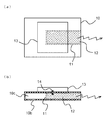
まず、本発明の実施例1について図面を用いて詳細に説明する。図2は、本実施例1による無線アンテナ基板10を示しており、図2(a)は正面図、図2(b)は断面図である。本実施例1による無線アンテナ基板10は板状であって、基板の周囲を囲む周囲導体10bとその内部を充填する誘電体10cとを含む。誘電体10cは、例えばポリテトラフルオロエチレン等の誘電体である。誘電体10cの一部には、壁部材11によって形成された導波路12が設けられている。壁部材11は、周囲導体10bと電気的に接続された導体であり、図2(a)に示すように連続的に形成される構造又は伝送する信号の波長よりも小さい間隔で導体を間欠的に配置する構造でも良い。導波路12は、壁部材11と周囲導体10bとに囲まれた閉空間となっており、かつ図示上右側の端面のみ周囲導体10bが形成されていない開放面を有している。このような構造によって、この内部に入力された電波又は信号は、開放面以外の部分から外部には漏出しないように構成されている。
First, Embodiment 1 of the present invention will be described in detail with reference to the drawings. 2A and 2B show the
無線アンテナ基板10の主面は部品搭載面となり、この上に無線モジュール13が載置されている。無線モジュール13の下面に設けられた給電部14は、導波路12内部に突出するように接続されている。導波路12は、給電部14からの入力を受けて共振器として振る舞い、開放面から電波を放出するアンテナとしての役割を果たす。このような構成とすることによって、電波の送受信を行うアンテナ面が端面側に設けられて無線モジュール13の搭載面と直交する方向となるため、無線アンテナ基板10の占有面積を小さくすることが可能となる。
The main surface of the
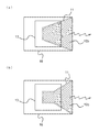
次に、本実施例1による無線アンテナ基板10の変形例について説明する。図3は、本実施例1による無線アンテナ基板10の変形例を示しており、図3(a)は第1の変形例、図3(b)は第2の変形例である。第1の変形例では、壁部材11が開放面側に向けて幅が広くなる略台形断面状に設けられた略台形導波路12bを形成している。第2の変形例では、壁部材11が中間部までは略矩形断面状でその後略台形断面状に設けられたいわゆるホーンアンテナ状導波路12cを形成している。このように形成することによって、第1の実施例による略台形導波路12b及び第2の実施例によるホーンアンテナ状導波路12cは、いずれも無線モジュール13から発信される電波をより広角度に放射することが可能となる。
Next, a modification of the
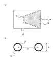
次に、本実施例1の第3の変形例について説明する。図4は、本実施例1による第3の変形例を示している。第3の変形例では、導波路12を形成する壁部材の代わりに複数の貫通孔15が等間隔に設けられている。貫通孔15は、図4(b)に示すように、直径dを有して距離D毎に設けられる。貫通孔15は内面に導体15bが被覆されるか又は導体15dの円筒を挿入して構成されており、無線アンテナ基板10の周囲導体10bと電気的に接続されている。2つの貫通孔の間の距離Dは、伝送する電波の波長λよりも十分に小さく、貫通孔15の直径dは距離Dよりも小さいものが用いられる。このような構成とすることによって、伝送される電波は、2つの貫通孔15の間を通過することができなくなる。つまり、複数の貫通孔15は擬似的な壁面とみなすことができる。複数の貫通孔15を設ける構造は、無線アンテナ基板10を製造した後に加工することが可能なため、製造工程が簡略化できるとともに、製造コストを削減することも可能となる。
Next, a third modification of the first embodiment will be described. FIG. 4 shows a third modification according to the first embodiment. In the third modification, a plurality of through
以上のような構成とすることによって、本実施例1による無線アンテナ基板10によれば、無線アンテナ基板10の端面を放射面とする導波路アンテナ構造を無線アンテナ基板10の内部に形成することによって、無線アンテナ基板10の上面に無線モジュール13を搭載しても全体の面積を小さくすることを実現できる。
With the configuration as described above, according to the
次に、本発明の実施例2について図面を用いて説明する。図5は、本実施例2による無線アンテナモジュール20を示す平面図である。本実施例2による無線アンテナモジュール20は、周囲を囲み筐体となる周囲導体と、無線モジュール23と、無線モジュール23の周囲を充填する誘電体と、外部の電子機器と接続されるコネクタ25とを含む。誘電体は、例えばポリテトラフルオロエチレン等である。誘電体には、壁部材21によって形成された導波路22が設けられている。壁部材21は、周囲導体と電気的に接続された導体であり、連続的に形成される構造、又は図4(b)に示すような伝送する信号の波長よりも小さい間隔Dで複数の貫通孔を配置する構造でも良い。導波路22は、壁部材21と周囲導体とに囲まれた閉空間となっており、かつ図示上右側の端面のみ周囲導体が形成されていない開放面を有している。このような構造によって、この内部に入力された電波又は信号は、開放面以外の部分から外部には漏出しないように構成されている。
Next,
無線モジュール23は、周囲導体の内部に設けられており、無線モジュール23に設けられた給電部24が、導波路22内部に突出するように接続されている。導波路22は、給電部24からの入力を受けて共振器として振る舞い、開放面から電波を放出するアンテナとしての役割を果たす。また、無線モジュール23は、その上面が周囲導体の上面と一致するように配置することもできる。コネクタ25は、無線アンテナモジュール20の表面にコネクタ端子が配置されるように設けられており、無線アンテナモジュール20の内部で無線モジュール23と電気的に接続されている。このような構成とすることによって、電波の送受信を行うアンテナ面が端面側に設けられるため、無線アンテナモジュール20の占有面積を小さくすることが可能となる。
The
また、図5に示した無線アンテナモジュール20は、図5(b)に示すように、導波路の放射面とコネクタとを相対する面に設けたカード型モジュールとして形成することによって、例えばパーソナルコンピュータ30等の機器への取り付け部31をスロット形状とすることも可能である。すなわち、無線モジュール及びアンテナがカード型の筐体内部に収納されることによって、取り付けられる機器側の接続部の構成も簡略化することが可能となる。
Further, as shown in FIG. 5B, the
以上のような構成とすることによって、本実施例2による無線アンテナモジュール20によれば、無線アンテナモジュール20の端面を放射面とする導波路アンテナ構造を無線アンテナモジュール20の内部に形成し、無線モジュール23及びコネクタ25を筐体となる周囲導体内部に設けることによって、無線アンテナモジュール20全体の面積を小さくすることを実現できる。また、本実施例2による無線アンテナモジュール20によれば、取り付けられる機器側の接続部の構成の簡略化も実現できる。
With the configuration as described above, according to the
以上の実施例から、本発明によれば、アンテナ面が基板の側端面に位置することから、基板の表面が自由に利用できる。例えば、基板表面に無線モジュールを搭載しても全体の面積を小さくすることが可能である。 From the above embodiments, according to the present invention, since the antenna surface is located on the side end surface of the substrate, the surface of the substrate can be used freely. For example, even if a wireless module is mounted on the substrate surface, the entire area can be reduced.
以上、説明した実施例は、本発明を実施するための最良の形態の一つにすぎず、本発明はその主旨を逸脱しない限り種々変化及び変形して実施可能である。 The embodiment described above is only one of the best modes for carrying out the present invention, and the present invention can be implemented with various changes and modifications without departing from the gist thereof.
10 無線アンテナ基板
10b 周囲導体
10c 誘電体
11、21 壁部材
12、12b、12c、22 導波路
13、23 無線モジュール
14、24 給電部
15 貫通孔
d 貫通孔15の直径
D 2つの貫通孔15の間の距離
λ 伝送される電波の波長
DESCRIPTION OF
Claims (7)
Priority Applications (1)
| Application Number | Priority Date | Filing Date | Title |
|---|---|---|---|
| JP2004102412A JP2005294883A (en) | 2004-03-31 | 2004-03-31 | Radio antenna |
Applications Claiming Priority (1)
| Application Number | Priority Date | Filing Date | Title |
|---|---|---|---|
| JP2004102412A JP2005294883A (en) | 2004-03-31 | 2004-03-31 | Radio antenna |
Publications (1)
| Publication Number | Publication Date |
|---|---|
| JP2005294883A true JP2005294883A (en) | 2005-10-20 |
Family
ID=35327389
Family Applications (1)
| Application Number | Title | Priority Date | Filing Date |
|---|---|---|---|
| JP2004102412A Pending JP2005294883A (en) | 2004-03-31 | 2004-03-31 | Radio antenna |
Country Status (1)
| Country | Link |
|---|---|
| JP (1) | JP2005294883A (en) |
Cited By (9)
| Publication number | Priority date | Publication date | Assignee | Title |
|---|---|---|---|---|
| JP2010278976A (en) * | 2009-06-01 | 2010-12-09 | National Institute Of Information & Communication Technology | Mm-wave antenna |
| JP2011109438A (en) * | 2009-11-18 | 2011-06-02 | Amushisu:Kk | Antenna module and radio device having the antenna module |
| JP2013179449A (en) * | 2012-02-28 | 2013-09-09 | Toshiba Corp | Radio device and information processing device and memory device including the same |
| JP2013247491A (en) * | 2012-05-25 | 2013-12-09 | Nippon Telegr & Teleph Corp <Ntt> | Mmic package integrating horn antenna and array antenna |
| JP2014075682A (en) * | 2012-10-04 | 2014-04-24 | Mitsubishi Electric Corp | Substrate integrated antenna module |
| US9166298B2 (en) | 2012-08-24 | 2015-10-20 | Kabushiki Kaisha Toshiba | Wireless device, and information processing apparatus and storage device including the wireless device |
| JP2016208495A (en) * | 2015-04-21 | 2016-12-08 | 京セラ株式会社 | Antenna board |
| JP2018046440A (en) * | 2016-09-15 | 2018-03-22 | 京セラ株式会社 | Antenna substrate |
| WO2024087841A1 (en) * | 2022-10-26 | 2024-05-02 | 深圳Tcl数字技术有限公司 | Millimeter-wave antenna assembly and display device |
-
2004
- 2004-03-31 JP JP2004102412A patent/JP2005294883A/en active Pending
Cited By (9)
| Publication number | Priority date | Publication date | Assignee | Title |
|---|---|---|---|---|
| JP2010278976A (en) * | 2009-06-01 | 2010-12-09 | National Institute Of Information & Communication Technology | Mm-wave antenna |
| JP2011109438A (en) * | 2009-11-18 | 2011-06-02 | Amushisu:Kk | Antenna module and radio device having the antenna module |
| JP2013179449A (en) * | 2012-02-28 | 2013-09-09 | Toshiba Corp | Radio device and information processing device and memory device including the same |
| JP2013247491A (en) * | 2012-05-25 | 2013-12-09 | Nippon Telegr & Teleph Corp <Ntt> | Mmic package integrating horn antenna and array antenna |
| US9166298B2 (en) | 2012-08-24 | 2015-10-20 | Kabushiki Kaisha Toshiba | Wireless device, and information processing apparatus and storage device including the wireless device |
| JP2014075682A (en) * | 2012-10-04 | 2014-04-24 | Mitsubishi Electric Corp | Substrate integrated antenna module |
| JP2016208495A (en) * | 2015-04-21 | 2016-12-08 | 京セラ株式会社 | Antenna board |
| JP2018046440A (en) * | 2016-09-15 | 2018-03-22 | 京セラ株式会社 | Antenna substrate |
| WO2024087841A1 (en) * | 2022-10-26 | 2024-05-02 | 深圳Tcl数字技术有限公司 | Millimeter-wave antenna assembly and display device |
Similar Documents
| Publication | Publication Date | Title |
|---|---|---|
| CN113889764B (en) | Dielectric resonator antenna module | |
| KR102505800B1 (en) | Wireless communication device with leaky wave phased array antenna | |
| JP4980306B2 (en) | Wireless communication device | |
| JP5712964B2 (en) | Antenna device | |
| CN110785893A (en) | Antenna modules and communication devices | |
| US7038622B2 (en) | Slot antenna array using LTCC technology | |
| JP7747654B2 (en) | Horn Antenna | |
| JP2014075682A (en) | Substrate integrated antenna module | |
| JPWO2018186065A1 (en) | High frequency module | |
| JP2006033699A (en) | Combination wireless unit-antenna and manufacturing method of combination wireless unit-antenna | |
| CN104185926B (en) | Antenna device | |
| KR101901101B1 (en) | Print type dipole antenna and electric device using the same | |
| JP2005294883A (en) | Radio antenna | |
| CN109728414B (en) | An antenna structure and terminal equipment | |
| WO2016056190A1 (en) | Antenna device | |
| JP2007013311A (en) | Antenna module and wireless apparatus | |
| JP2004072320A (en) | Antenna system | |
| US12308526B2 (en) | Array antenna | |
| KR20050075966A (en) | Omnidirectional antenna | |
| EP3918664B1 (en) | Redirecting structure for electromagnetic waves | |
| JP4227589B2 (en) | Active array antenna | |
| WO2020253938A1 (en) | Continuous beam steering antenna structure | |
| JP2018148334A (en) | Slot antenna | |
| JP4181085B2 (en) | Dielectric waveguide antenna | |
| WO2017168705A1 (en) | Antenna |
Legal Events
| Date | Code | Title | Description |
|---|---|---|---|
| A621 | Written request for application examination |
Effective date: 20060913 Free format text: JAPANESE INTERMEDIATE CODE: A621 |
|
| A977 | Report on retrieval |
Effective date: 20080516 Free format text: JAPANESE INTERMEDIATE CODE: A971007 |
|
| A131 | Notification of reasons for refusal |
Effective date: 20080527 Free format text: JAPANESE INTERMEDIATE CODE: A131 |
|
| A521 | Written amendment |
Free format text: JAPANESE INTERMEDIATE CODE: A523 Effective date: 20080701 |
|
| A131 | Notification of reasons for refusal |
Free format text: JAPANESE INTERMEDIATE CODE: A131 Effective date: 20081209 |
|
| A521 | Written amendment |
Effective date: 20090130 Free format text: JAPANESE INTERMEDIATE CODE: A523 |
|
| A02 | Decision of refusal |
Free format text: JAPANESE INTERMEDIATE CODE: A02 Effective date: 20090512 |