JP2005294861A - Semiconductor memory device and its manufacturing method - Google Patents
Semiconductor memory device and its manufacturing method Download PDFInfo
- Publication number
- JP2005294861A JP2005294861A JP2005155956A JP2005155956A JP2005294861A JP 2005294861 A JP2005294861 A JP 2005294861A JP 2005155956 A JP2005155956 A JP 2005155956A JP 2005155956 A JP2005155956 A JP 2005155956A JP 2005294861 A JP2005294861 A JP 2005294861A
- Authority
- JP
- Japan
- Prior art keywords
- thin film
- film
- concentration impurity
- insulating film
- gate
- Prior art date
- Legal status (The legal status is an assumption and is not a legal conclusion. Google has not performed a legal analysis and makes no representation as to the accuracy of the status listed.)
- Pending
Links
- 239000004065 semiconductor Substances 0.000 title claims abstract description 71
- 238000004519 manufacturing process Methods 0.000 title claims abstract description 49
- 238000005530 etching Methods 0.000 claims abstract description 89
- VYPSYNLAJGMNEJ-UHFFFAOYSA-N Silicium dioxide Chemical compound O=[Si]=O VYPSYNLAJGMNEJ-UHFFFAOYSA-N 0.000 claims abstract description 20
- 229910052814 silicon oxide Inorganic materials 0.000 claims abstract description 20
- 239000010408 film Substances 0.000 claims description 238
- 239000010409 thin film Substances 0.000 claims description 99
- 229910052581 Si3N4 Inorganic materials 0.000 claims description 64
- HQVNEWCFYHHQES-UHFFFAOYSA-N silicon nitride Chemical compound N12[Si]34N5[Si]62N3[Si]51N64 HQVNEWCFYHHQES-UHFFFAOYSA-N 0.000 claims description 64
- 239000012535 impurity Substances 0.000 claims description 41
- 238000000034 method Methods 0.000 claims description 35
- 238000002955 isolation Methods 0.000 claims description 24
- 239000000758 substrate Substances 0.000 claims description 20
- 230000015572 biosynthetic process Effects 0.000 claims description 17
- 239000004020 conductor Substances 0.000 claims description 9
- 239000011159 matrix material Substances 0.000 claims description 2
- 238000009751 slip forming Methods 0.000 claims 3
- 238000009792 diffusion process Methods 0.000 abstract description 31
- 230000010354 integration Effects 0.000 abstract description 11
- 238000005468 ion implantation Methods 0.000 abstract description 8
- 230000003647 oxidation Effects 0.000 abstract description 7
- 238000007254 oxidation reaction Methods 0.000 abstract description 7
- 239000010410 layer Substances 0.000 description 32
- 238000005516 engineering process Methods 0.000 description 19
- 239000000463 material Substances 0.000 description 14
- 229910021420 polycrystalline silicon Inorganic materials 0.000 description 14
- 229920005591 polysilicon Polymers 0.000 description 14
- 238000005229 chemical vapour deposition Methods 0.000 description 12
- 229910052785 arsenic Inorganic materials 0.000 description 10
- RQNWIZPPADIBDY-UHFFFAOYSA-N arsenic atom Chemical compound [As] RQNWIZPPADIBDY-UHFFFAOYSA-N 0.000 description 10
- 238000010438 heat treatment Methods 0.000 description 5
- WNUPENMBHHEARK-UHFFFAOYSA-N silicon tungsten Chemical compound [Si].[W] WNUPENMBHHEARK-UHFFFAOYSA-N 0.000 description 5
- 238000000151 deposition Methods 0.000 description 4
- 238000010586 diagram Methods 0.000 description 4
- 230000002093 peripheral effect Effects 0.000 description 4
- OAICVXFJPJFONN-UHFFFAOYSA-N Phosphorus Chemical compound [P] OAICVXFJPJFONN-UHFFFAOYSA-N 0.000 description 2
- XUIMIQQOPSSXEZ-UHFFFAOYSA-N Silicon Chemical compound [Si] XUIMIQQOPSSXEZ-UHFFFAOYSA-N 0.000 description 2
- 230000012447 hatching Effects 0.000 description 2
- 238000009413 insulation Methods 0.000 description 2
- 238000000059 patterning Methods 0.000 description 2
- 239000011574 phosphorus Substances 0.000 description 2
- 229910052698 phosphorus Inorganic materials 0.000 description 2
- 229910052710 silicon Inorganic materials 0.000 description 2
- 239000010703 silicon Substances 0.000 description 2
- XAGFODPZIPBFFR-UHFFFAOYSA-N aluminium Chemical compound [Al] XAGFODPZIPBFFR-UHFFFAOYSA-N 0.000 description 1
- 229910052782 aluminium Inorganic materials 0.000 description 1
- 238000000137 annealing Methods 0.000 description 1
- HAYXDMNJJFVXCI-UHFFFAOYSA-N arsenic(5+) Chemical compound [As+5] HAYXDMNJJFVXCI-UHFFFAOYSA-N 0.000 description 1
- 230000005684 electric field Effects 0.000 description 1
- 239000011229 interlayer Substances 0.000 description 1
- 238000004518 low pressure chemical vapour deposition Methods 0.000 description 1
- 238000002161 passivation Methods 0.000 description 1
- 230000000630 rising effect Effects 0.000 description 1
- 239000002356 single layer Substances 0.000 description 1
- WQJQOUPTWCFRMM-UHFFFAOYSA-N tungsten disilicide Chemical compound [Si]#[W]#[Si] WQJQOUPTWCFRMM-UHFFFAOYSA-N 0.000 description 1
- 229910021342 tungsten silicide Inorganic materials 0.000 description 1
Images


Landscapes
- Semiconductor Memories (AREA)
- Non-Volatile Memory (AREA)
Abstract
Description
この発明は、半導体記憶装置およびその製造方法に関し、特に、半導体記憶装置を高密度化するためのSAS(Self Aligned Source)技術に関する。 The present invention relates to a semiconductor memory device and a manufacturing method thereof, and more particularly, to a SAS (Self Aligned Source) technique for increasing the density of a semiconductor memory device.
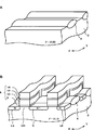
フラッシュEPROMなど不揮発性半導体記憶装置のメモリアレイを高密度化するための方法として、SAS技術が知られている。図24A〜図25Bに基づいて、SAS技術を用いたメモリアレイの製造方法を説明する。まず、図24Aに示すように、半導体基板2の上にX方向を長手方向とするストライプ状に、素子分離のためのフィールド酸化膜4を形成する。
SAS technology is known as a method for increasing the density of a memory array of a nonvolatile semiconductor memory device such as a flash EPROM. A memory array manufacturing method using the SAS technology will be described with reference to FIGS. 24A to 25B. First, as shown in FIG. 24A, a
つぎに、図24Bに示すように、ストライプ状のフィールド酸化膜4に直交するストライプ状(Y方向を長手方向とするストライプ状)に、積層ゲート6を形成する。積層ゲート6は、メモリセル(図25BのメモリセルMC参照)のチャネル形成領域CH上に、ゲート酸化膜8、フローティングゲート10、ONO膜12、コントロールゲート14をこの順に積層した構造を備えている。
Next, as shown in FIG. 24B, the
積層ゲート6のうち、ゲート酸化膜8、フローティングゲート10およびONO膜12は、各メモリセルごとに独立しているが、コントロールゲート14は、同一列を構成するメモリセル(Y方向に並んだ複数のメモリセル)をつなぐように形成されている。
Among the
つぎに、積層ゲート6およびフィールド酸化膜4に対して自己整合的にドレインDおよび、低濃度ソースLSを形成する。ドレインDおよび低濃度ソースLSは、それぞれ、行方向(X方向)に隣接する2つのメモリセル間で共用される。
Next, the drain D and the low concentration source LS are formed in a self-aligned manner with respect to the stacked
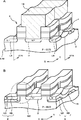
つぎに、図25Aに示すように、ドレインDを覆うようにレジスト16を形成し、レジスト16および積層ゲート6をマスクとしてシリコン酸化物に対する選択性の高いエッチングをおこなう。このエッチングをSASエッチングと呼ぶ。このSASエッチングによって、列方向(Y方向)に隣接する低濃度ソースLS間に介在していたフィールド酸化膜4が、選択的に除去される。
Next, as shown in FIG. 25A, a
この状態で、高濃度のヒ素(As)をイオン注入する。したがって、高濃度のヒ素は、行方向に隣接するメモリセル間で共用されるソース形成領域と、当該ソース形成領域を列方向につなぐ領域すなわち先程のSASエッチングによってフィールド酸化膜4が除去された領域とに注入される。
In this state, high concentration arsenic (As) is ion-implanted. Therefore, high-concentration arsenic is a source formation region shared between memory cells adjacent in the row direction and a region connecting the source formation region in the column direction, that is, a region where the
この後、加熱することにより、図25Bに示すように、メモリセルの高濃度ソースHSをY方向に連結した構造の拡散ソース配線15が形成される。このようにして、積層ゲート6に対し自己整合的に、拡散ソース配線15を形成することができる。これが、SAS技術である。SAS技術を用いることにより、半導体記憶装置の集積度を向上させることができる。
Thereafter, by heating, a
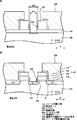
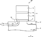
しかし、上記のSAS技術には、次のような問題点がある。図26に拡大して示すように、SASエッチングの際、メモリセルMCのゲート酸化膜8の端部やソースSの表面がある程度浸食されてしまう。
However, the above SAS technology has the following problems. As shown in an enlarged view in FIG. 26, during the SAS etching, the end portion of the
これでは、メモリセルMCに対する書込みや消去の際に重要な役割を果すゲートエッジ部19の形状や表面状態が不安定になっしまう。すなわち、メモリセルMCに対する書込みや消去に要する電圧や、当該電圧の印加時間に大きなバラ付きを生ずる。
This makes the shape and surface state of the
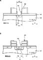
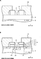
このような問題を解決するために、図27A〜図28Bに示すような改良されたSAS技術が提案されている(特開平7−312395参照)。図27A、図28Aは、図25Aの断面27Aに対応する部分の断面図であり、改良されたSAS技術にかかるものである。図27B、図28Bは、図25Aの断面27Bに対応する部分の断面図であり、改良されたSAS技術にかかるものである。
In order to solve such a problem, an improved SAS technology as shown in FIGS. 27A to 28B has been proposed (see Japanese Patent Laid-Open No. 7-312395). 27A and 28A are cross-sectional views of a portion corresponding to the
改良されたSAS技術においては、積層ゲート6を形成した後、積層ゲート6に対し自己整合的に、低濃度ソースLS、高濃度ソースHS、ドレインDを形成し、その後、SASエッチングする前に、図27Aおよび図27Bに示すように、積層ゲート6の側面にシリコン酸化物で構成されたサイドウォール18を形成する。
In the improved SAS technology, after forming the
サイドウォール18は、周辺回路を構成するLDD(Lightly Doped Drain)型のMOSFETを形成する工程において同時に形成される。すなわち、CVD法(化学的気相成長法)等によりシリコン酸化物を堆積させ、その後、異方性エッチングを行なう(エッチバックする)ことで、サイドウォール18が形成される。したがって、サイドウォール18は、X方向にかなりの厚さを有する厚膜となる。
The
その後、図28Aおよび図28Bに示すように、SASエッチングを行なう。サイドウォール18は、SASエッチングに際してある程度浸食されるものの、図28Bに示すように、ゲートエッジ部19の近傍は、SASエッチング終了に至るまで、サイドウォール18によって保護される。
Thereafter, as shown in FIGS. 28A and 28B, SAS etching is performed. Although the
その後、レジスト16、積層ゲート6および取り残されたサイドウォール18をマスクとして、高濃度のヒ素(As)をイオン注入し、加熱する。これにより、図29に平面図で示すように、メモリセルの高濃度ソースHSをY方向に連結した構造の拡散ソース配線15が形成される。
Thereafter, high-concentration arsenic (As) is ion-implanted and heated using the
しかしながら、上記のような従来のSAS技術にも、次のような問題点がある。上記のように改良されたSAS技術を用いることによって、図28Bに示すゲートエッジ部19はSASエッチングから保護されるものの、図29に示すように、拡散ソース配線15の幅が、部分的に狭く(幅w1)なってしまう。
However, the conventional SAS technology as described above has the following problems. Although the
これは、取り残されたサイドウォール18をマスクとして、高濃度のヒ素(As)をイオン注入するため、ヒ素イオンの注入幅が、当該サイドウォール18の幅(通常1500〜2000オングストローム程度)の2倍(3000〜4000オングストローム程度)に相当する分だけ、狭くなってしまうからである。
This is because ion implantation of high-concentration arsenic (As) is performed using the
したがって、幅の狭い部分がネックとなり、拡散ソース配線15の電気抵抗が大きくなってしまう。このため、特に、データの書込み等に際し大きなソース電流を流すタイプのメモリに適用した場合、各メモリ素子間で、電圧降下によるソース電位のバラ付きが大きくなり、動作が不安定になるおそれがある。
Therefore, the narrow portion becomes a bottleneck, and the electric resistance of the
このような場合、隣接する積層ゲート6の間隙w2を大きくすれば、幅w1も大きくなるため、このような問題は解決されるが、間隙w2を大きくすることにより、メモリの集積度が犠牲になってしまう。たとえば、0.35μm(3500オングストローム)のデザインルールを用いたメモリにおいて、間隙w2を3000〜4000オングストローム程度広げるとなると、メモリ素子部分の集積度は、1/2程度に落ちてしまう。
In such a case, if the gap w2 between the adjacent stacked
この発明は、このような問題点を解決し、集積度が高く、かつ、動作時の信頼性の高い半導体記憶装置およびその製造方法を提供することを目的とする。 An object of the present invention is to solve such problems and to provide a semiconductor memory device having a high degree of integration and high reliability during operation and a method for manufacturing the same.
請求項1の半導体記憶装置の製造方法においては、実質的に積層ゲートの側面を覆う絶縁性薄膜を形成し、選択エッチングによって、実質的に積層ゲートに対して自己整合的に素子分離用絶縁膜を除去し、素子分離用絶縁膜の除去された半導体領域を含む半導体領域に、実質的に積層ゲートに対して自己整合的に第1の高濃度不純物領域を形成することを特徴としている。 2. The method of manufacturing a semiconductor memory device according to claim 1, wherein an insulating thin film that substantially covers the side surface of the stacked gate is formed, and the insulating film for element isolation is substantially self-aligned with the stacked gate by selective etching. And a first high-concentration impurity region is formed in the semiconductor region including the semiconductor region from which the element isolation insulating film is removed substantially in a self-aligned manner with respect to the stacked gate.
したがって、積層ゲートを構成する下部絶縁膜の側面は絶縁性薄膜に覆われているため、選択エッチングによって浸食されることはない。このため、書込み時等動作時の信頼性が高い。 Therefore, since the side surface of the lower insulating film constituting the stacked gate is covered with the insulating thin film, it is not eroded by the selective etching. For this reason, the reliability at the time of operation, such as writing, is high.
また、絶縁性薄膜の厚さを薄く設定することにより、積層ゲートおよび絶縁性薄膜をマスクとして第1の高濃度不純物領域を形成する際、第1の高濃度不純物領域の幅の減少量を小さく抑えることができる。このため、隣接する積層ゲートの間隙を大きくすることなく、第1の高濃度不純物領域について所定幅を確保することができる。この結果、集積度を犠牲にすることなく、列方向に連続的に形成される第1の高濃度不純物領域の電気抵抗の増大を防ぐことができる。 In addition, by reducing the thickness of the insulating thin film, when the first high concentration impurity region is formed using the stacked gate and the insulating thin film as a mask, the amount of reduction in the width of the first high concentration impurity region is reduced. Can be suppressed. Therefore, a predetermined width can be secured for the first high-concentration impurity region without increasing the gap between adjacent stacked gates. As a result, it is possible to prevent an increase in electric resistance of the first high-concentration impurity region formed continuously in the column direction without sacrificing the degree of integration.
すなわち、集積度が高く、かつ、動作時の信頼性が高い半導体記憶装置を実現することができる。 In other words, it is possible to realize a semiconductor memory device having a high degree of integration and high reliability during operation.
請求項2の半導体記憶装置の製造方法においては、絶縁性薄膜を、シリコン酸化物を主成分とする薄膜としたことを特徴としている。
The method of manufacturing a semiconductor memory device according to
したがって、熱酸化法やCVD法(化学的気相成長法)などにより、薄い絶縁膜を容易に得ることができる。 Therefore, a thin insulating film can be easily obtained by a thermal oxidation method or a CVD method (chemical vapor deposition method).
請求項3の半導体記憶装置の製造方法においては、絶縁性薄膜を、シリコン窒化物を主成分とする薄膜としたことを特徴としている。 The method of manufacturing a semiconductor memory device according to claim 3 is characterized in that the insulating thin film is a thin film mainly composed of silicon nitride.
したがって、選択エッチングにおいてエッチングされにくいシリコン窒化物を用いることで、素子分離用絶縁膜の厚さに対する積層ゲートの高さの比率がより小さくなった場合であっても、選択エッチングにおいて、下部絶縁膜の側面を保護することができる。また、選択エッチングにおいて、積層ゲートの側面全体を保護することができるので、動作時の信頼性を、より高めることができる。 Therefore, even when the ratio of the height of the stacked gate to the thickness of the element isolation insulating film becomes smaller by using silicon nitride that is difficult to be etched in the selective etching, the lower insulating film is used in the selective etching. Can protect the sides. In addition, since the entire side surface of the stacked gate can be protected in the selective etching, the reliability during operation can be further improved.
請求項4の半導体記憶装置の製造方法においては、積層ゲートを形成した後、メモリアレイ部全体にシリコン窒化物を主成分とする薄膜を堆積し、異方性エッチングにより、堆積した厚さ分だけ当該薄膜を除去することにより、少なくとも選択エッチングによって除去すべき素子分離用絶縁膜の上にある当該薄膜を除去し、その後、選択エッチングを行なうことを特徴としている。 According to another aspect of the semiconductor memory device manufacturing method of the present invention, after the stacked gate is formed, a thin film mainly composed of silicon nitride is deposited on the entire memory array portion, and an anisotropic etching is performed for the deposited thickness. By removing the thin film, at least the thin film over the element isolation insulating film to be removed by selective etching is removed, and then selective etching is performed.
したがって、素子分離用絶縁膜の上にあるシリコン窒化物を主成分とする薄膜を除去して、当該素子分離用絶縁膜を露出させておくことにより、その後の選択エッチングによって、素子分離用絶縁膜を容易に除去することができる。 Therefore, by removing the thin film mainly composed of silicon nitride on the element isolation insulating film and exposing the element isolation insulating film, the element isolation insulating film is obtained by subsequent selective etching. Can be easily removed.
請求項5の半導体記憶装置の製造方法においては、絶縁性薄膜を、シリコン酸化物を主成分とし実質的に積層ゲートの側面を覆う第1の薄膜、およびシリコン窒化物を主成分とし実質的に第1の薄膜を覆う第2の薄膜、を用いて構成したことを特徴としている。 6. The method of manufacturing a semiconductor memory device according to claim 5, wherein the insulating thin film is substantially composed of silicon oxide as a main component, a first thin film substantially covering a side surface of the laminated gate, and silicon nitride as a main component. The second thin film covering the first thin film is used.
したがって、電荷を捕獲しにくいシリコン酸化物を主成分とする第1の薄膜を用いて積層ゲートの側面を覆うことで、積層ゲートの側面において不用意に電荷が捕獲されるのを防止することができる。また、選択エッチングにおいてエッチングされにくいシリコン窒化物を主成分とする第2の薄膜を用いて第1の薄膜を覆うことで、選択エッチングにおいて、確実に下部絶縁膜の側面を保護することができる上、積層ゲートの側面全体を保護することができる。このため、動作時の信頼性を、さらに高めることができる。 Therefore, by covering the side surface of the stacked gate with the first thin film mainly composed of silicon oxide that does not easily trap charges, it is possible to prevent the charge from being inadvertently captured on the side surface of the stacked gate. it can. Further, by covering the first thin film with the second thin film mainly composed of silicon nitride which is difficult to be etched in the selective etching, the side surface of the lower insulating film can be reliably protected in the selective etching. The entire side surface of the stacked gate can be protected. For this reason, the reliability at the time of operation | movement can further be improved.
請求項6の半導体記憶装置の製造方法においては、積層ゲートを形成する際、上部導電体層の上にさらにシリコン窒化物を主成分とする第3の薄膜を形成しておき、その後、実質的に積層ゲートの側面を覆うように第1の薄膜を形成し、その後、メモリアレイ部全体に前記第2の薄膜を堆積し、異方性エッチングにより、堆積した厚さ分だけ当該第2の薄膜を除去することにより、少なくとも選択エッチングによって除去すべき素子分離用絶縁膜の上にある第2の薄膜を除去し、その後、選択エッチングを行なうことを特徴としている。
In the method of manufacturing a semiconductor memory device according to
つまり、上記異方性エッチング前においては、積層ゲートの側面に形成された第1の薄膜の側面および上部は、第2の薄膜により覆われている。したがって、異方性エッチングにより、堆積した厚さ分だけ当該第2の薄膜を除去したとしても、第1の薄膜の側面および上部が露出することはない。このため、その後に行なわれる選択エッチングにおいて、第1の薄膜が浸食されることはない。すなわち、積層ゲートの側面を覆う第1の薄膜と、第1の薄膜を覆う第2の薄膜とを用いて構成される絶縁性薄膜を、容易に得ることができる。 That is, before the anisotropic etching, the side surface and the upper portion of the first thin film formed on the side surface of the stacked gate are covered with the second thin film. Therefore, even if the second thin film is removed by anisotropic etching by the deposited thickness, the side surface and the upper part of the first thin film are not exposed. For this reason, in the selective etching performed thereafter, the first thin film is not eroded. That is, it is possible to easily obtain an insulating thin film that is configured by using the first thin film that covers the side surface of the stacked gate and the second thin film that covers the first thin film.
請求項7の半導体記憶装置の製造方法においては、絶縁性薄膜の厚さを、下部絶縁膜の厚さと同程度の厚さないし下部絶縁膜の厚さの10倍程度の厚さとしたことを特徴としている。 The method of manufacturing a semiconductor memory device according to claim 7 is characterized in that the thickness of the insulating thin film is not as thick as the thickness of the lower insulating film or about 10 times the thickness of the lower insulating film. It is said.
したがって、第1の高濃度不純物領域から下部絶縁膜を介して下部導電体層に流れるべき電流が、絶縁性薄膜を介して下部導電体層に流れる可能性は極めて低く、かつ、第1の高濃度不純物領域の幅の減少量を小さく抑えることができる。すなわち、絶縁性薄膜の絶縁性を確保しつつ、第1の高濃度不純物領域の幅の減少量を小さく抑えることができる。 Therefore, it is very unlikely that the current that should flow from the first high-concentration impurity region to the lower conductor layer via the lower insulating film flows to the lower conductor layer via the insulating thin film. The amount of decrease in the width of the concentration impurity region can be kept small. That is, the amount of decrease in the width of the first high-concentration impurity region can be kept small while ensuring the insulating properties of the insulating thin film.
請求項8の半導体記憶装置の製造方法においては、選択エッチングの後、素子分離用絶縁膜の除去された半導体領域を含む半導体領域に、実質的に積層ゲートおよび除去されなかった素子分離用絶縁膜に対して自己整合的に、第1の高濃度不純物領域および第2の高濃度不純物領域を形成することを特徴としている。
9. The method of manufacturing a semiconductor memory device according to
したがって、第2の高濃度不純物領域、および、列方向に連続的に形成される第1の高濃度不純物領域を、同一工程で形成することが可能となる。このため、マスク工程等煩雑な工程を伴う不純物導入工程の数を低減することができる。すなわち、製造コストを低減することができる。 Therefore, the second high-concentration impurity region and the first high-concentration impurity region formed continuously in the column direction can be formed in the same process. For this reason, it is possible to reduce the number of impurity introduction steps involving complicated steps such as a mask step. That is, the manufacturing cost can be reduced.
請求項9の半導体記憶装置においては、積層ゲートの側面を少なくとも実質的に下部絶縁膜の上端まで覆う高さの絶縁性薄膜を備えたことを特徴としている。したがって、書込み等の動作時に重要な役割を果す下部絶縁膜の側面近傍を絶縁性薄膜で覆って保護することにより、より確実に、書込み等の動作の信頼性を高めることができる。 According to another aspect of the semiconductor memory device of the present invention, an insulating thin film having a height that covers at least substantially the side surface of the stacked gate to the upper end of the lower insulating film is provided. Therefore, by covering and protecting the vicinity of the side surface of the lower insulating film that plays an important role during the operation such as writing with the insulating thin film, the reliability of the operation such as writing can be more reliably improved.
なお、請求項において、「半導体基板に半導体領域を設ける」とは、半導体基板に接して半導体領域を形成する場合、半導体基板の上に形成した一層以上の別の層の上に半導体領域を形成する場合、および、半導体基板自体が半導体領域である場合を含む概念である。 In the claims, “providing a semiconductor region on a semiconductor substrate” means that when a semiconductor region is formed in contact with the semiconductor substrate, the semiconductor region is formed on one or more other layers formed on the semiconductor substrate. This is a concept including a case where the semiconductor substrate itself is a semiconductor region.
本発明の構成によれば、積層ゲートを構成する下部絶縁膜の側面は絶縁性薄膜に覆われているため、選択エッチングによって浸食されることはない。このため、書込み時等動作時の信頼性が高い。また、絶縁性薄膜の厚さを薄く設定することにより、積層ゲートおよび絶縁性薄膜をマスクとして第1の高濃度不純物領域を形成する際、第1の高濃度不純物領域の幅の減少量を小さく抑えることができる。このため、隣接する積層ゲートの間隙を大きくすることなく、第1の高濃度不純物領域について所定幅を確保することができる。この結果、集積度を犠牲にすることなく、列方向に連続的に形成される第1の高濃度不純物領域の電気抵抗の増大を防ぐことができる。すなわち、集積度が高く、かつ、動作時の信頼性が高い半導体記憶装置を実現することができる。 According to the configuration of the present invention, since the side surface of the lower insulating film constituting the stacked gate is covered with the insulating thin film, it is not eroded by the selective etching. For this reason, the reliability at the time of operation, such as writing, is high. In addition, by reducing the thickness of the insulating thin film, when the first high concentration impurity region is formed using the stacked gate and the insulating thin film as a mask, the amount of reduction in the width of the first high concentration impurity region is reduced. Can be suppressed. Therefore, a predetermined width can be secured for the first high-concentration impurity region without increasing the gap between adjacent stacked gates. As a result, it is possible to prevent an increase in electric resistance of the first high-concentration impurity region formed continuously in the column direction without sacrificing the degree of integration. In other words, it is possible to realize a semiconductor memory device having a high degree of integration and high reliability during operation.
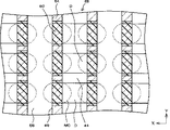
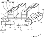
[第1の実施形態]図12に、この発明の一実施形態による半導体記憶装置であるフラッシュEPROMのメモリアレイ部の平面構成を概念的に表わした図面を示す。このフラッシュEPROMは、不揮発性の半導体記憶装置であり、メモリアレイ部26には、複数のメモリセルMC(図12において、破線で囲んだ部分)が、直交する行列状に配置されている。なお、メモリセルMCのX方向の並びを行、Y方向の並びを列と呼ぶ。
[First Embodiment] FIG. 12 conceptually shows a planar configuration of a memory array portion of a flash EPROM which is a semiconductor memory device according to an embodiment of the present invention. This flash EPROM is a non-volatile semiconductor memory device, and a plurality of memory cells MC (portions surrounded by broken lines in FIG. 12) are arranged in an orthogonal matrix form in the
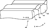
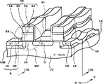
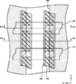
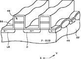
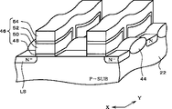
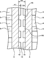
図6に、メモリアレイ部26の一部を表わす斜視図を示す。メモリセルMCは、P型(第1導電型)の半導体基板22(半導体領域)に設定されたチャネル形成領域CHと、チャネル形成領域CHを挟んで配置されたN型(第2導電型)のソースSおよびドレインD(第2の高濃度不純物領域)と、チャネル形成領域CHの上に形成された積層ゲート46を備えている。
FIG. 6 is a perspective view showing a part of the
ソースSは、N+型の高濃度ソースHSと、高濃度ソースHSを取り囲むように形成されたN-型の低濃度ソースLS(低濃度不純物領域)とを備えている。ドレインDおよびソースSは、それぞれ、行方向(X方向)に隣接する2つのメモリセル間で共用される。メモリセルのソースSのうち高濃度ソースHSは、列方向(Y方向)に連結され、拡散ソース配線55(第1の高濃度不純物領域)となっている。異なる行に属するメモリセルのドレインDは、フィールド酸化膜44(第1の素子分離用絶縁膜)によって電気的に分離されている。 The source S includes an N + type high concentration source HS and an N − type low concentration source LS (low concentration impurity region) formed so as to surround the high concentration source HS. The drain D and the source S are respectively shared between two memory cells adjacent in the row direction (X direction). Of the source S of the memory cell, the high concentration source HS is connected in the column direction (Y direction) to form a diffusion source wiring 55 (first high concentration impurity region). The drains D of the memory cells belonging to different rows are electrically isolated by a field oxide film 44 (first element isolation insulating film).
また、積層ゲート46は、ゲート酸化膜48(下部絶縁膜)、フローティングゲート50(下部導電体層)、ONO膜52(上部絶縁膜)、コントロールゲート54(上部導電体層)をこの順に積層した構成を備えている。積層ゲート46のうち、ゲート酸化膜48、フローティングゲート50およびONO膜52は、各メモリセルごとに独立しているが、コントロールゲート54は、同一列を構成するメモリセル(Y方向に並んだ複数のメモリセル)をつなぐように形成されている。なお、図12の右上がりのハッチング部(細線)がコントロールゲート54を表わし、右下がりのハッチング部(太線)がフローティングゲート50を表わす。
The
積層ゲート46の側面には、絶縁用薄膜である熱酸化膜58が形成されている。熱酸化膜58の厚さは、特に限定されるものではないが、ゲート酸化膜48の厚さと同程度の厚さないしゲート酸化膜48の厚さの10倍程度の厚さとするのが好ましい。この程度の厚さにすれば、ソースSからゲート酸化膜48を介してフローティングゲート50に流れるべき電流が、熱酸化膜58を介してフローティングゲート50に流れる可能性は極めて低く、かつ、拡散ソース配線55の幅の減少量を小さく抑えることができるからである。たとえば、ゲート酸化膜48の厚さを100オングストローム程度とすると、熱酸化膜58の厚さを100〜1000オングストローム程度にするのが好ましい。
A
熱酸化膜58の膜厚制御が容易であれば、より好ましくは、熱酸化膜58の厚さを、ゲート酸化膜48の厚さと同程度の厚さないしゲート酸化膜48の厚さの5倍程度の厚さ(上述の例では、100〜500オングストローム程度)とするのがよい。さらに好ましくは、熱酸化膜58の厚さを、ゲート酸化膜48の厚さと同程度の厚さないしゲート酸化膜48の厚さの2倍程度の厚さ(上述の例では、100〜200オングストローム程度)とするのがよい。
If the film thickness control of the
すなわち、熱酸化膜58の厚さは、熱酸化膜58を介してフローティングゲート50に流れる電流が無視できる程度の厚さであれば、薄いほうがよいことになる。
In other words, the thickness of the
ソースS側の熱酸化膜58は、後述するSASエッチングによりある程度除去されるものの、ゲート酸化膜48の側面を覆う程度には残存している。
Although the
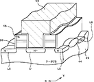
つぎに、このフラッシュEPROMの製造方法について説明する。図1〜図6は、この発明の一実施形態による半導体記憶装置であるフラッシュEPROMの製造工程を説明するための斜視図である。図7A〜図10Bは、各工程における主要部分の断面図である。 Next, a method for manufacturing the flash EPROM will be described. 1 to 6 are perspective views for explaining a manufacturing process of a flash EPROM which is a semiconductor memory device according to an embodiment of the present invention. 7A to 10B are cross-sectional views of main parts in the respective steps.
フラッシュEPROMを製造するには、図1R>1に示すように、まず、P型の半導体基板22を用意し、LOCOS法を用いて、メモリアレイ部26の素子分離領域42上に、フィールド酸化膜44を形成する。フィールド酸化膜44は、X方向を長手方向とするストライプ状に形成される。
In order to manufacture a flash EPROM, as shown in FIG. 1R> 1, first, a P-
なお、この実施形態においては、約1000℃の水蒸気雰囲気中で加熱することにより、3000オングストローム程度の膜厚を有するフィールド酸化膜44を形成している。
In this embodiment, the
つぎに、図2に示すように、ストライプ状のフィールド酸化膜44に直交するストライプ状(Y方向を長手方向とするストライプ状)に、積層ゲート46を形成する。積層ゲート46は、つぎのようにして形成する。
Next, as shown in FIG. 2, the
まず、半導体基板22の露出した素子形成領域40(図1参照)の表面に、ゲート酸化膜48となる熱酸化膜を形成する。なお、この実施形態においては、約900℃の乾燥雰囲気中で加熱することにより、当該熱酸化膜を形成するようにしている。
First, a thermal oxide film to be a
この上に、フローティングゲート50となるポリシリコン層を、X方向を長手方向とするストライプ状に形成する。この実施形態においては、当該ポリシリコン層を、約620℃の温度下でCVD法を用いて形成している。ポリシリコン層形成後、不純物であるリンを該ポリシリコン層にドープしておく。このポリシリコン層を覆うように、ONO膜52となるONO層を形成する。
On this, a polysilicon layer to be the floating
つぎに、コントロールゲート54となるポリシリコン層およびタングステンシリサイド(WSi)層を形成する。この実施形態においては、当該ポリシリコン層を、約620℃の温度下でCVD法を用いて形成している。最後に、このポリシリコン層、タングステンシリサイド(WSi)層および上述のONO層、X方向を長手方向とするストライプ状のポリシリコン層、熱酸化膜をパタニングすることによって、積層ゲート46が形成される。
Next, a polysilicon layer and a tungsten silicide (WSi) layer to be the
なお、この実施形態においては、積層ゲート46を構成する各層の厚さを、次のように設定している。すなわち、ゲート酸化膜48の厚さ:約100オングストローム、フローティングゲート50の厚さ:約1000オングストローム、ONO膜52の厚さ:約200オングストローム、コントロールゲートの厚さ:約3000オングストローム(内、タングステンシリサイドの厚さ:約1500オングストローム)である。
In this embodiment, the thickness of each layer constituting the stacked
つぎに、積層ゲート46に対して自己整合的に、N-型の低濃度ソースLSおよびN+型のドレインDを形成する。低濃度ソースLSを形成するために、ドレインDとなるべき領域をレジスト(図示せず)で覆った後、低濃度ソースLSとなるべき領域に低濃度のリン(P)を注入する。ドレインDを形成するために、低濃度ソースLSとなるべき領域をレジスト(図示せず)で覆った後、ドレインDとなるべき領域に高濃度のヒ素(As)を注入する。その後、アニール(加熱)工程を経て、低濃度ソースLSおよびドレインDが形成される。
Next, an N− type low concentration source LS and an N + type drain D are formed in a self-aligned manner with respect to the stacked
上述のように、低濃度ソースLSおよびドレインDは、それぞれ、行方向(X方向)に隣接する2つのメモリセル間で共用される。 As described above, the low-concentration source LS and the drain D are shared between two memory cells adjacent in the row direction (X direction).
なお、低濃度ソースLSおよびドレインDの形成工程と前後して、周辺回路を構成するNチャンネル型MOSFETやPチャンネル型MOSFET(図示せず)のLDD(Lightly Doped Drain)領域を形成しておく。 Before and after the process of forming the low concentration source LS and the drain D, an LDD (Lightly Doped Drain) region of an N channel type MOSFET or a P channel type MOSFET (not shown) constituting the peripheral circuit is formed.
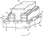
つぎに、図3に示すように、熱酸化を行なうことにより、積層ゲート46の上面および側面に、熱酸化膜58を形成する。絶縁性薄膜として熱酸化膜58を用いれば、膜厚の制御が容易である上、膜組織が緻密であるため絶縁性に優れており、好都合である。
Next, as shown in FIG. 3, a
この実施形態においては、熱酸化膜58の厚さを、200オングストローム程度、すなわち、ゲート酸化膜48の2倍程度の厚さに設定している。
In this embodiment, the thickness of the
したがって、ソースSからゲート酸化膜48を介してフローティングゲート50に流れるべき電流が、熱酸化膜58を介してフローティングゲートに流れる可能性は極めて低く、かつ、拡散ソース配線55の幅の減少量を小さく抑えることができる。すなわち、熱酸化膜58の絶縁性を確保しつつ、拡散ソース配線55の幅の減少量を小さく抑えることができる。
Therefore, the possibility that the current that should flow from the source S to the floating
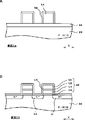
図3における断面7Aを図7Aに示す。また、図3における断面7Bを図7Bに示す。図7Bに示すように、熱酸化膜58は、積層ゲート46の上面および側面全体を覆うように形成されている。なお、半導体基板22のうち露出した部分にも、熱酸化膜58が形成される。
A
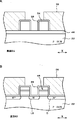
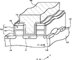
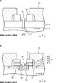
つぎに、図4に示すように、ドレインDおよび、積層ゲート46の一部を覆うように、Y方向を長手方向とするストライプ状に、レジスト56を形成する。図4における断面8Aを図8Aに示す。また、図4における断面8Bを図8Bに示す。
Next, as shown in FIG. 4, a resist 56 is formed in a stripe shape with the Y direction as the longitudinal direction so as to cover the drain D and part of the stacked
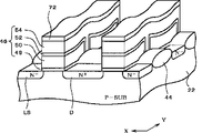
つぎに、図5に示すように、レジスト56、積層ゲート46および熱酸化膜58をマスクとしてシリコン酸化物に対する選択性の高い異方性エッチング(SASエッチング)を行なう。図5における断面9Aを図9Aに示す。また、図5における断面9Bを図9Bに示す。
Next, as shown in FIG. 5, anisotropic etching (SAS etching) with high selectivity to silicon oxide is performed using resist 56, stacked
図9Aに示すように、SASエッチングによって、低濃度ソースLS(図4参照)間にあったフィールド酸化膜44が、選択的に除去される。上述のように、積層ゲート46の側面に形成される熱酸化膜58の膜厚が薄いため、図9Aに示すように、除去されるフィールド酸化膜44の幅w3は、隣接する積層ゲート46の間隙w2に比し、それほど狭くなっていない。
As shown in FIG. 9A, the
SASエッチングに際し、フィールド酸化膜44と同時に、露出した熱酸化膜58も高さ方向に浸食され、図9Bのように、背が低くなる。しかし、SASエッチングは、上述のように、異方性エッチングであるから、高さ方向に直交する方向(図中X方向、およびY方向)には、あまり浸食されない。一方、上述のように、フィールド酸化膜44の膜厚(3000オングストローム程度)に比し、積層ゲート46の厚さ(4300オングストローム程度)がかなり厚い。
During the SAS etching, the exposed
したがって、フィールド酸化膜44の除去が終了した時点でも、熱酸化膜58は、ある程度残存することになる。つまり、SASエッチングが終了するまで、積層ゲート46のゲートエッジ部59は、熱酸化膜58によって覆われていることになる。
Accordingly, even when the removal of the
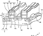
SASエッチングが終了すると、つぎに、レジスト56、積層ゲート46、および取り残された熱酸化膜58をマスクとして、高濃度のヒ素(As)をイオン注入する。上述のように、熱酸化膜58の膜厚が薄いため、イオン注入の際のマスクとしての熱酸化膜58のX方向の寸法(すなわち膜厚)は、SASエッチングの場合と同様に、ほとんど問題とならない。
When the SAS etching is completed, high concentration arsenic (As) is then ion-implanted using the resist 56, the stacked
イオン注入された部分を、図9Aおよび図9R>9Bの×印で示す。すなわち、図5に示すように、高濃度のヒ素は、低濃度ソースLSと、当該低濃度ソースLSをY方向につなぐ領域すなわち先程のSASエッチングによってフィールド酸化膜44が除去された領域とに注入される。
The ion-implanted portion is indicated by a cross in FIGS. 9A and 9R> 9B. That is, as shown in FIG. 5, high-concentration arsenic is implanted into the low-concentration source LS and the region connecting the low-concentration source LS in the Y direction, that is, the region where the
この後、レジスト56をはく離し、加熱することにより、図6に示すように、メモリセルの高濃度ソースHSが形成されるとともに、高濃度ソースHSをY方向に連結した構造の拡散ソース配線55が形成される。このようにして、実質的に積層ゲート46に対し自己整合的に、拡散ソース配線55を形成することができる。図6における断面10Aを図10Aに示す。また、図6における断面10Bを図10Bに示す。図10Aに示すように、拡散ソース配線55の幅w4は、隣接する積層ゲート46の間隙w2と同等程度あるいはそれ以上でであることが分る。
Thereafter, the resist 56 is peeled off and heated to form the high concentration source HS of the memory cell as shown in FIG. 6, and the
この後、上述の周辺回路を構成するNチャンネル型MOSFETやPチャンネル型MOSFET(図示せず)のゲート側面にサイドウォールが形成され、ゲートおよび該サイドウォールをマスクとして、該Nチャンネル型MOSFETのN+型のソース/ドレインやPチャンネル型MOSFETのP+型のソース/ドレインが形成される。 Thereafter, a sidewall is formed on the gate side surface of the N-channel MOSFET or P-channel MOSFET (not shown) constituting the peripheral circuit described above, and N of the N-channel MOSFET is formed using the gate and the sidewall as a mask. A + type source / drain and a P + type source / drain of a P channel type MOSFET are formed.
なお、周辺回路を構成するNチャンネル型MOSFETやPチャンネル型MOSFETのゲート側面にサイドウォールが形成される際、同時に、メモリセルの積層ゲート46の両側にも、サイドウォール(図示せず)が形成される。
When sidewalls are formed on the gate side surfaces of N-channel MOSFETs and P-channel MOSFETs constituting the peripheral circuit, sidewalls (not shown) are also formed on both sides of the stacked
最後に、図示しないが、層間膜形成工程、コンタクト形成工程、アルミ配線工程、パッシベーション膜形成工程等を経て、フラッシュEPROMが製造される。 Finally, although not shown, a flash EPROM is manufactured through an interlayer film forming process, a contact forming process, an aluminum wiring process, a passivation film forming process, and the like.
このように、この実施形態においては、積層ゲート46の側面を覆う熱酸化膜58を形成し、選択エッチングによって、実質的に積層ゲート46に対して自己整合的にフィールド酸化膜44を除去し、フィールド酸化膜44の除去された領域を含む半導体基板22に、実質的に積層ゲート46に対して自己整合的に、高濃度ソースHSをY方向に連結した構造の拡散ソース配線55を形成するようにしている。
Thus, in this embodiment, the
したがって、ゲート酸化膜48の側面を含むゲートエッジ部59(図9B参照)は熱酸化膜58に覆われているため、選択エッチングによって浸食されることはない。このため、メモリセルへの書込み時等動作時の信頼性が高い。
Therefore, since the gate edge portion 59 (see FIG. 9B) including the side surface of the
また、熱酸化膜58の膜厚が薄いので、積層ゲート46および該熱酸化膜58をマスクとして拡散ソース配線55を形成する際、拡散ソース配線55の幅の減少を抑制することができる。このため、隣接する積層ゲート46の間隙を大きくすることなく、拡散ソース配線55について所定幅を確保することができる。この結果、集積度を犠牲にすることなく、列方向に連続的に形成される拡散ソース配線55の電気抵抗の増大を防ぐことができる。
Further, since the
すなわち、集積度が高く、かつ、動作時の信頼性が高いフラッシュEPROM等のメモリ装置を実現することができる。 That is, a memory device such as a flash EPROM having a high degree of integration and high reliability during operation can be realized.
なお、この実施形態においては、絶縁性薄膜として、熱酸化膜58を用いたが、絶縁性薄膜として、シリコン酸化物を主成分とする薄膜であって熱酸化膜以外の薄膜、たとえば、CVD(化学的気相成長)法を用いて形成したシリコン酸化膜を用いてもよい。CVD法を用いてシリコン酸化膜を成膜することにより、比較的低温下で、容易にシリコン酸化膜を得ることができる。
In this embodiment, the
また、この実施形態においては、絶縁性薄膜として、シリコン酸化物を主成分とする薄膜を用いたが、絶縁性薄膜はこれに限定されるものではない。たとえば、絶縁性薄膜として、シリコン窒化物を主成分とする薄膜を用いることもできる。 In this embodiment, a thin film mainly composed of silicon oxide is used as the insulating thin film, but the insulating thin film is not limited to this. For example, a thin film mainly composed of silicon nitride can be used as the insulating thin film.
[第2の実施形態]絶縁性薄膜として、シリコン窒化物を主成分とする薄膜を用いた場合の製造方法の一例を、図13〜図16を用いて説明する。 [Second Embodiment] An example of a manufacturing method using a thin film mainly composed of silicon nitride as an insulating thin film will be described with reference to FIGS.
積層ゲート46を形成するまでの工程は、上述の実施形態と同様である(図1、図2参照)。その後、図13に示すように、絶縁性薄膜として、シリコン窒化膜68を形成する。シリコン窒化膜68は、CVD法を用いて、シリコン窒化物を薄膜状に堆積させることにより成膜する。
The steps until the stacked
したがって、積層ゲート46の側面のみならず、積層ゲート46の上面、露出した半導体基板22の上部、および、フィールド酸化膜44の上部に、薄膜状のシリコン窒化膜68が形成されることになる。なお、この実施形態においては、シリコン窒化膜68の膜厚を200オングストローム程度に設定しているが、上述の実施形態の場合と同様に、シリコン窒化膜68の膜厚は、特に限定されるものではない。
Therefore, a thin
つぎに、図14に示すように、ドレインDおよび、積層ゲート46の一部を覆うように、Y方向を長手方向とするストライプ状に、レジスト56を形成する。その後、レジスト56をマスクとして、シリコン窒化物に対する選択性の高い異方性エッチングを行ない、シリコン窒化膜68の膜厚分だけ、シリコン窒化膜68を除去する。これにより、フィールド酸化膜44の上部のシリコン窒化膜68が除去される。フィールド酸化膜44の上部にシリコン窒化膜68があると、次工程のSASエッチングにおいて、フィールド酸化膜44を除去できないからである。なお、露出した積層ゲート46の上面および半導体基板22の上部に形成されたシリコン窒化膜68も、同時に除去される。
Next, as shown in FIG. 14, a resist 56 is formed in a stripe shape with the Y direction as the longitudinal direction so as to cover the drain D and part of the stacked
つぎに、図15に示すように、レジスト56、積層ゲート46および側面に残されたシリコン窒化膜68をマスクとしてシリコン酸化物に対する選択性の高いSASエッチングを行なう。
Next, as shown in FIG. 15, SAS etching with high selectivity to silicon oxide is performed using the resist 56, the
図15に示すように、SASエッチングによって、低濃度ソースLS間にあったフィールド酸化膜44(図14参照)が、選択的に除去される。 As shown in FIG. 15, the field oxide film 44 (see FIG. 14) existing between the low-concentration sources LS is selectively removed by SAS etching.
絶縁性薄膜として熱酸化膜58を用いた上述の実施形態の場合と異なり、この実施形態においては、SASエッチングに際し、絶縁性薄膜であるシリコン窒化膜68はほとんど浸食されない。
Unlike the above-described embodiment using the
このように、SASエッチングにおいてエッチングされにくいシリコン窒化膜68を絶縁性薄膜として用いれば、仮に、フィールド酸化膜44の厚さに対する積層ゲート46の高さの比率がより小さくなった場合であっても、SASエッチングにおいて、積層ゲート46のゲートエッジ部59が露出することはなく、確実にゲートエッジ部59を保護することができる。また、SASエッチングにおいて、ONO膜52の側面を含め積層ゲート46の側面全体を保護することができるので、動作時の信頼性を、より高めることができる。
As described above, if the
SASエッチング終了後の工程は、前述の実施形態の場合と、ほぼ同様である。すなわち、レジスト56、積層ゲート46およびその側面に残されたシリコン窒化膜68をマスクとして、高濃度のヒ素(As)をイオン注入し、その後、レジスト56をはく離し、加熱することにより、図16に示すように、メモリセルの高濃度ソースHSが形成されるとともに、高濃度ソースHSをY方向に連結した構造の拡散ソース配線55が形成される。このようにして、前述の実施形態と同様に、実質的に積層ゲート46に対し自己整合的に、拡散ソース配線55を形成することができるのである。
The process after the SAS etching is completed is almost the same as that in the above-described embodiment. That is, high-concentration arsenic (As) is ion-implanted using the resist 56, the
[第3の実施形態]図17〜図22は、この発明のさらに他の実施形態による半導体記憶装置であるフラッシュEPROMの製造工程を説明するための斜視図である。この実施形態においては、絶縁性薄膜78として、第1の薄膜である熱酸化膜74および第2の薄膜であるシリコン窒化膜76を用いている。
[Third Embodiment] FIGS. 17 to 22 are perspective views for explaining a manufacturing process of a flash EPROM which is a semiconductor memory device according to still another embodiment of the present invention. In this embodiment, a
フィールド酸化膜44を形成する工程までは、上述の各実施形態と同様である(図1参照)。その後、図17に示すように、ストライプ状の積層ゲート46を形成するが、この実施形態においては、積層ゲート46の上部にシリコン窒化物により構成された第3の薄膜であるキャップ材72を形成するようにしている。キャップ材72を形成することにより、後述するように、SASエッチングにおいて、熱酸化膜74が浸食されるのを防止することができる(図21参照)。
The process up to the formation of the
積層ゲート46およびキャップ材72を形成する手順を説明する。コントロールゲート54となるポリシリコン層およびタングステンシリサイド(WSi)層を堆積させる工程までは、上述の実施形態と同様である。すなわち、ゲート酸化膜48となる熱酸化膜、フローティングゲート50となるポリシリコン層、ONO膜52となるONO層、コントロールゲート54となるポリシリコン層およびタングステンシリサイド(WSi)層を、この順に形成する。
A procedure for forming the
その後、キャップ材72となるシリコン窒化膜を、減圧CVD法等を用いて堆積させる。この実施形態においては、当該シリコン窒化膜の膜厚を800オングストローム程度に設定している。
Thereafter, a silicon nitride film to be the
つぎに、このシリコン窒化膜、ポリシリコン層およびタングステンシリサイド(WSi)層、ONO層、X方向を長手方向とするストライプ状のポリシリコン層、熱酸化膜をパタニングすることによって、積層ゲート46ならびにキャップ材72が形成される。なお、積層ゲート46を構成する各層の厚さは、上述の実施形態と同様であるが、特に限定されるものではない。
Next, by patterning the silicon nitride film, the polysilicon layer and the tungsten silicide (WSi) layer, the ONO layer, the stripe-like polysilicon layer whose longitudinal direction is the X direction, and the thermal oxide film, the stacked
つぎに、積層ゲート46に対して自己整合的に、N-型の低濃度ソースLSおよびN+型のドレインDを形成するが、この工程は、上述の実施形態と同様である。
Next, an N− type low concentration source LS and an N + type drain D are formed in a self-aligned manner with respect to the stacked
つぎに、図18に示すように、熱酸化を行なうことにより、積層ゲート46の側面に、熱酸化膜74を形成する。第1の薄膜として熱酸化膜74を用いれば、膜厚の制御が容易である上、膜組織が緻密であるため絶縁性に優れており、好都合である。
Next, as shown in FIG. 18, a
図18に示すように、熱酸化膜74は、半導体基板22のうち露出したシリコン部分にも形成される一方、シリコン窒化物で構成されたキャップ材72の側面や上部には、ほとんど形成されない。したがって、キャップ材72の側面等に極めて薄く熱酸化膜が形成されたとしても、実用上ほとんど問題はない。ただし、極く軽くエッチングを行なうことで、キャップ材72の側面等に形成された極く薄い熱酸化膜を除去するようにすれば、なおよい。
As shown in FIG. 18, the
その後、図19に示すように、第2の薄膜として、シリコン窒化膜76を形成する。シリコン窒化膜76は、CVD法を用いて、シリコン窒化物を薄膜状に堆積させることにより成膜する。
Thereafter, as shown in FIG. 19, a
したがって、積層ゲート46の側面に形成された上述の熱酸化膜74を覆うように、薄膜状のシリコン窒化膜76が形成されることになる。なお、キャップ材72の側面および上面、半導体基板22上に形成された熱酸化膜76の上部、ならびに、フィールド酸化膜44の上部にも、薄膜状のシリコン窒化膜76が形成されることになる。
Therefore, a thin
なお、この実施形態においては、熱酸化膜74の厚さを、100オングストローム程度とし、シリコン窒化膜76の膜厚を100オングストローム程度に設定している。すなわち、熱酸化膜74とシリコン窒化膜76とを合せた絶縁性薄膜78の厚さを200オングストローム程度に設定している。ただし、上述の各実施形態の場合と同様に、これら各膜厚は、特に限定されるものではない。
In this embodiment, the thickness of the
つぎに、図20に示すように、レジスト56を形成し、レジスト56をマスクとして、シリコン窒化物に対する選択性の高い異方性エッチングを行ない、シリコン窒化膜76の膜厚分だけ、シリコン窒化膜76を除去する。これにより、フィールド酸化膜44の上部のシリコン窒化膜76が除去される。
Next, as shown in FIG. 20, a resist 56 is formed, and anisotropic etching with high selectivity to silicon nitride is performed using the resist 56 as a mask, and the silicon nitride film is formed by the thickness of the
上述のように、積層ゲート46の側面に形成された熱酸化膜74の側面は、シリコン窒化膜76により覆われている。また、キャップ材72の側面(すなわち、積層ゲート46の側面に形成された熱酸化膜74の上部)にも、シリコン窒化膜76が形成されている。
As described above, the side surface of the
したがって、上記異方性エッチングによって、堆積した厚さ分だけシリコン窒化膜76を除去したとしても、積層ゲート46の側面に形成された熱酸化膜74の側面および上面が露出することはない。
Therefore, even if the
このため、その後に行なわれるSASエッチングにおいて、積層ゲート46の側面に形成された熱酸化膜74が浸食されることはない。すなわち、キャップ材72を形成しておくことにより、積層ゲート46の側面を覆う熱酸化膜74と、熱酸化膜74を覆うシリコン窒化膜76とを用いて構成される絶縁性薄膜78を、容易に得ることができるのである。
Therefore, in the subsequent SAS etching, the
なお、露出したキャップ材72の上面および半導体基板22上に形成された熱酸化膜76の上部に形成されたシリコン窒化膜76も、上記異方性エッチングによって、同時に除去される。
Note that the
つぎに、図21に示すように、レジスト56、キャップ材72、残された絶縁性薄膜78をマスクとしてシリコン酸化物に対する選択性の高いSASエッチングを行なう。
Next, as shown in FIG. 21, SAS etching with high selectivity to silicon oxide is performed using the resist 56, the
図21に示すように、SASエッチングによって、低濃度ソースLS間にあったフィールド酸化膜44(図20参照)が、選択的に除去される。一方、絶縁性薄膜78は、外側がシリコン窒化膜76により構成されているため、SASエッチングに際し、ほとんど浸食されない。
As shown in FIG. 21, the field oxide film 44 (see FIG. 20) existing between the low-concentration sources LS is selectively removed by SAS etching. On the other hand, since the insulating
このように、この実施形態においては、絶縁性薄膜78を、実質的に積層ゲート46の側面を覆う熱酸化膜74、および該熱酸化膜74を覆うシリコン窒化膜76を用いて構成している。
Thus, in this embodiment, the insulating
したがって、シリコン窒化膜に比し電荷をトラップ(捕獲)しにくい熱酸化膜74を用いて積層ゲート46の側面を直接覆うことで、フローティングゲート50に取込まれるべき電荷、あるいはフローティングゲート50から排出されるべき電荷が、不用意に絶縁性薄膜にトラップされるのを防止することができる。このため、電荷がトラップされることによる電界の好まざる変動(すなわち、書込み時、消去時等における不安定動作の発生)を防止することができる。
Therefore, by directly covering the side surface of the stacked
また、SASエッチングにおいてエッチングされにくいシリコン窒化膜76を用いて熱酸化膜74を覆うことで、SASエッチングにおいて、確実にゲートエッジ部59を保護することができる。また、SASエッチングにおいて、ONO膜52の側面を含め積層ゲート46の側面全体を保護することができるので、動作時の信頼性を、さらに高めることができる。
Further, by covering the
SASエッチング終了後の工程は、前述の各実施形態の場合と、ほぼ同様である。すなわち、レジスト56、キャップ材72、積層ゲート46の側面に残された絶縁性薄膜78をマスクとして、高濃度のヒ素(As)をイオン注入し、その後、レジスト56をはく離し、加熱することにより、図22に示すように、メモリセルの高濃度ソースHSが形成されるとともに、高濃度ソースHSをY方向に連結した構造の拡散ソース配線55が形成される。このようにして、前述の各実施形態と同様に、実質的に積層ゲート46に対し自己整合的に、拡散ソース配線55を形成することができるのである。
The steps after the SAS etching are almost the same as those in the above-described embodiments. That is, high-concentration arsenic (As) is ion-implanted using the resist 56, the
[その他の実施形態]なお、図13〜図16に示す実施形態、および、図17〜図22に示す実施形態においては、レジスト56を形成した後、シリコン窒化膜68またはシリコン窒化膜76を、その膜厚分だけ除去するようにしたが、シリコン窒化膜68またはシリコン窒化膜76をその膜厚分だけ除去する工程は、レジスト56形成後に限定されるものではない。たとえば、レジスト56形成前に、シリコン窒化膜68またはシリコン窒化膜76をその膜厚分だけ除去する工程を実施するようにしてもよい。
[Other Embodiments] In the embodiments shown in FIGS. 13 to 16 and the embodiments shown in FIGS. 17 to 22, after the resist 56 is formed, the
また、上述の各実施形態においては、SASエッチングを行なう前に、低濃度ソースLSおよびドレインDを形成するとともに、SASエッチング終了後に、高濃度ソースHSをY方向に連結した構造の拡散ソース配線55を形成するよう構成したが、低濃度ソースLS、ドレインD、拡散ソース配線55を形成する手順は、これに限定されるものではない。たとえば、ドレインDおよび拡散ソース配線55を同一工程で形成するようにしてもよい。
In each of the above-described embodiments, the low concentration source LS and the drain D are formed before the SAS etching, and the high concentration source HS is connected in the Y direction after the SAS etching is finished. However, the procedure for forming the low concentration source LS, the drain D, and the
ドレインDおよび拡散ソース配線55を同一工程で形成する場合の一例を、図1〜図12に示す実施形態の場合を例に説明する。
An example of the case where the drain D and the
まず、図1に示すように、フィールド酸化膜44を形成したあと、積層ゲート46を形成する。その後、図23に示すように、積層ゲート46に対して自己整合的に、N-型の低濃度ソースLSのみを形成する。
First, as shown in FIG. 1, after forming a
その後、SASエッチング終了までの工程は、上記図1〜図12に示す実施形態の場合とほぼ同様である。ただし、本実施形態においては、SASエッチング終了後、レジスト56をはく離し、その後、積層ゲート46および残存するフィールド酸化膜44をマスクとして、高濃度のヒ素(As)をイオン注入するようにしている。
Thereafter, the processes up to the end of the SAS etching are substantially the same as those in the embodiment shown in FIGS. However, in this embodiment, after the SAS etching is completed, the resist 56 is peeled off, and then high concentration arsenic (As) is ion-implanted using the stacked
したがって、その後の加熱により、図6に示すように、ドレインDと、高濃度ソースHSをY方向に連結した構造の拡散ソース配線55とが、同時に形成される。
Therefore, by subsequent heating, as shown in FIG. 6, the drain D and the
このように、この実施形態においては、SASエッチングの後、フィールド酸化膜44の除去された半導体領域を含む半導体基板22に、実質的に積層ゲート46および除去されなかったフィールド酸化膜44に対して自己整合的に、拡散ソース配線55およびドレインDを形成するようにしている。
Thus, in this embodiment, after the SAS etching, the
したがって、ドレインD、および、高濃度ソースHSをY方向に連結した構造のソース配線55を、同一工程で形成することが可能となる。このため、マスク工程等煩雑な工程を伴うイオン打込み工程の数を低減することができる。すなわち、製造コストを低減することができる。
Therefore, the
なお、この実施形態のように、SASエッチングに用いたレジスト56を除去した後にイオン注入工程を実施するような場合には、イオン注入工程に先立ち、軽い熱酸化工程を実施しておくと、なおよい。熱酸化膜を形成することで、半導体基板22の表面や積層ゲート46の表面が、イオン注入の際にダメージを受けるのを防止できるからである。
If the ion implantation process is performed after removing the resist 56 used for the SAS etching as in this embodiment, a light thermal oxidation process is performed prior to the ion implantation process. Good. This is because the formation of the thermal oxide film can prevent the surface of the
また、この実施形態においては、低濃度ソースLSは、SASエッチングの前に形成するようにしたが、拡散ソース配線55およびドレインD同様、低濃度ソースLSも、SASエッチングの後に形成するようにしてもよい。この場合には、SASエッチングの後に低濃度ソースLSを形成し、その後に、拡散ソース配線55およびドレインDを形成する工程を実施することになる。
In this embodiment, the low-concentration source LS is formed before the SAS etching. However, the low-concentration source LS is also formed after the SAS etching, like the
逆に、従来のように、SASエッチングの前に、低濃度ソースLS、高濃度ソースHSおよびドレインDを形成しておき、SASエッチングの後で、高濃度ソースHSをつないで拡散ソース配線55にするための工程を実施するようにしてもよい。
Conversely, as in the prior art, the low concentration source LS, the high concentration source HS, and the drain D are formed before the SAS etching, and the high concentration source HS is connected to the
なお、上述の各実施形態においては、絶縁性薄膜として、熱酸化膜、CVDにより形成したシリコン酸化薄膜、シリコン窒化膜、熱酸化膜とシリコン窒化膜とを重ねた積層薄膜を例示したが、絶縁性薄膜はこれに限定されるものではない。絶縁性薄膜として、たとえば、シリコン酸化窒化膜(シリコン酸化物とシリコン窒化物とが混在する薄膜)や、3層以上の積層薄膜などを用いることもできる。また、上述の各実施形態においては、上部絶縁膜としてONO膜52を例に説明したが、上部絶縁膜はONO膜に限定されるものではない。たとえば、単層のシリコン酸化膜により構成される上部絶縁膜等を用いた半導体記憶装置にも適用することができる。
In each of the above embodiments, the insulating thin film is exemplified by a thermal oxide film, a silicon oxide thin film formed by CVD, a silicon nitride film, and a laminated thin film in which a thermal oxide film and a silicon nitride film are stacked. However, the conductive thin film is not limited to this. As the insulating thin film, for example, a silicon oxynitride film (thin film in which silicon oxide and silicon nitride are mixed), a laminated thin film having three or more layers, or the like can be used. In each of the above-described embodiments, the
なお、上述の実施形態においては、半導体記憶装置としてフラッシュEPROMを例に説明したが、この発明はフラッシュEPROMに限定されるものではない。 In the above-described embodiment, the flash EPROM has been described as an example of the semiconductor memory device, but the present invention is not limited to the flash EPROM.
44・・・・・・フィールド酸化膜
46・・・・・・積層ゲート
56・・・・・・レジスト
58・・・・・・熱酸化膜
59・・・・・・ゲートエッジ部
LS・・・・・・低濃度ソース
w2・・・・・・隣接する積層ゲート46の間隙
w3・・・・・・フィールド酸化膜44の幅
44 ···
Claims (9)
The following (A) to (C), (A) a first conductivity type channel formation region set in a semiconductor region provided on a semiconductor substrate, and (B) a second conductivity type disposed across the channel formation region. A stacked gate having the following (c1) to (c4) formed on the first high-concentration impurity region, the second high-concentration impurity region, and (C) the channel formation region, A stacked gate with an insulating thin film with a height that covers at least substantially the upper side of the lower insulating film, (c1) a lower insulating film formed on the channel formation region, and (c2) formed on the lower insulating film A plurality of memory cells having a plurality of memory cells, wherein: (c3) an upper insulating layer formed on the lower conductive layer; and (c4) an upper conductive layer formed on the upper insulating layer. Arranged memory array portion, upper conductor layer of memory cells belonging to same column The first high-concentration impurity region and the second high-concentration impurity region of each memory cell are continuously formed between the memory cells adjacent in the row direction, and the first high-concentration impurity region is The first high-concentration impurity regions of the memory cells belonging to two columns adjacent to each other are continuously formed in the column direction, and the first high-concentration impurity regions of the memory cells belonging to two columns adjacent to each other with the second high-concentration impurity regions interposed therebetween. 2. A semiconductor memory device comprising: a memory array portion in which the high-concentration impurity regions are electrically isolated from each other in a column direction by an element isolation insulating film.
Priority Applications (1)
| Application Number | Priority Date | Filing Date | Title |
|---|---|---|---|
| JP2005155956A JP2005294861A (en) | 2005-05-27 | 2005-05-27 | Semiconductor memory device and its manufacturing method |
Applications Claiming Priority (1)
| Application Number | Priority Date | Filing Date | Title |
|---|---|---|---|
| JP2005155956A JP2005294861A (en) | 2005-05-27 | 2005-05-27 | Semiconductor memory device and its manufacturing method |
Related Parent Applications (1)
| Application Number | Title | Priority Date | Filing Date |
|---|---|---|---|
| JP10187707A Division JP2000022114A (en) | 1998-07-02 | 1998-07-02 | Semiconductor storage device and its manufacture |
Publications (1)
| Publication Number | Publication Date |
|---|---|
| JP2005294861A true JP2005294861A (en) | 2005-10-20 |
Family
ID=35327371
Family Applications (1)
| Application Number | Title | Priority Date | Filing Date |
|---|---|---|---|
| JP2005155956A Pending JP2005294861A (en) | 2005-05-27 | 2005-05-27 | Semiconductor memory device and its manufacturing method |
Country Status (1)
| Country | Link |
|---|---|
| JP (1) | JP2005294861A (en) |
-
2005
- 2005-05-27 JP JP2005155956A patent/JP2005294861A/en active Pending
Similar Documents
| Publication | Publication Date | Title |
|---|---|---|
| JP4870719B2 (en) | Nonvolatile memory device having monosgate structure | |
| KR100829034B1 (en) | Nonvolatile Semiconductor Memory and Manufacturing Method Thereof | |
| US7005328B2 (en) | Non-volatile memory device | |
| US8865546B2 (en) | Method for manufacturing a non-volatile semiconductor memory device having contact plug formed on silicided source/drain region | |
| CN101164169B (en) | Method for forming array source lines in NAND flash memory | |
| CN1351382A (en) | Semiconductor storage array self-alignment method and manufactured storage array of floating gate memory cells with control gate spacers | |
| US7606073B2 (en) | Nonvolatile semiconductor memory with dummy cell which is absence of a source/drain region | |
| KR20020050115A (en) | Semiconductor memory device with silicide layer formed selectively | |
| US7015542B2 (en) | MONOS memory device | |
| US7091090B2 (en) | Nonvolatile memory device and method of forming same | |
| JP4818061B2 (en) | Nonvolatile semiconductor memory | |
| JP2000022114A (en) | Semiconductor storage device and its manufacture | |
| CN100440485C (en) | Manufacturing method of nonvolatile semiconductor memory device | |
| US6872624B2 (en) | Method of fabricating nonvolatile semiconductor memory device | |
| JP6880595B2 (en) | Semiconductor devices and their manufacturing methods | |
| US9299569B2 (en) | Manufacturing method of semiconductor device | |
| JP2019102520A (en) | Semiconductor device manufacturing method | |
| KR100351051B1 (en) | Method for fabricating non-volatile memory cell having bilayered structured floating gate | |
| US8093645B2 (en) | Non-volatile semiconductor memory device | |
| JP2005294861A (en) | Semiconductor memory device and its manufacturing method | |
| JP2004103945A (en) | Method for manufacturing semiconductor device | |
| US20030157758A1 (en) | Non-volatile semiconductor memory device and manufacturing method therefor | |
| US20040135196A1 (en) | Semiconductor device and method of manufacturing the same | |
| KR100940644B1 (en) | Semiconductor device and manufacturing method | |
| JP5415135B2 (en) | Nonvolatile semiconductor memory device |
Legal Events
| Date | Code | Title | Description |
|---|---|---|---|
| A977 | Report on retrieval |
Free format text: JAPANESE INTERMEDIATE CODE: A971007 Effective date: 20090316 |
|
| A131 | Notification of reasons for refusal |
Free format text: JAPANESE INTERMEDIATE CODE: A131 Effective date: 20090512 |
|
| A02 | Decision of refusal |
Free format text: JAPANESE INTERMEDIATE CODE: A02 Effective date: 20091027 |