JP2005294779A - LED light source - Google Patents
LED light source Download PDFInfo
- Publication number
- JP2005294779A JP2005294779A JP2004111791A JP2004111791A JP2005294779A JP 2005294779 A JP2005294779 A JP 2005294779A JP 2004111791 A JP2004111791 A JP 2004111791A JP 2004111791 A JP2004111791 A JP 2004111791A JP 2005294779 A JP2005294779 A JP 2005294779A
- Authority
- JP
- Japan
- Prior art keywords
- led
- light source
- led light
- resin
- substrate
- Prior art date
- Legal status (The legal status is an assumption and is not a legal conclusion. Google has not performed a legal analysis and makes no representation as to the accuracy of the status listed.)
- Pending
Links
Images
Classifications
-
- H10W90/724—
Landscapes
- Led Device Packages (AREA)
Abstract
Description
本発明は静電耐圧の高いLED光源に関する。 The present invention relates to an LED light source having a high electrostatic withstand voltage.
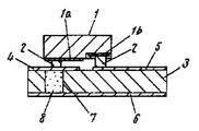
GaN系LEDは、GaAs系のLEDと比較して静電気に対する耐圧が低く、従来から多くの耐圧向上に関する検討が行われてきた。従来のLED光源(半導体発光装置)としては、高絶縁性の基板の表面に形成された正負の電極と半導体発光素子の正負の電極とをそれぞれ接続して構成された半導体発光装置において、基板内部に注入材注入部が形成され、その注入材注入部に所定の電気特性を有する注入材が注入され、正負の電極間が、注入材を介して接続されているものがあった(例えば、特許文献1)。図8は、特許文献1に記載された従来のLED光源を示すものである。 GaN-based LEDs have a lower withstand voltage against static electricity than GaAs-based LEDs, and many studies have been made on improving the withstand voltage. As a conventional LED light source (semiconductor light-emitting device), a semiconductor light-emitting device configured by connecting positive and negative electrodes formed on the surface of a highly insulating substrate and positive and negative electrodes of a semiconductor light-emitting element, respectively, An injection material injection portion is formed, an injection material having predetermined electrical characteristics is injected into the injection material injection portion, and positive and negative electrodes are connected via an injection material (for example, patents) Reference 1). FIG. 8 shows a conventional LED light source described in Patent Document 1. In FIG.
図8において、発光素子は1、基板は3、貫通孔は7、注入材は8、電極パタンは4、5で示される。
しかしながら、LED1個あたりの光量は少なく、特に照明などの用途に使用するには、多数のLEDを使用する必要がある。このため、LED数が多くなるとLED1個ごとに基板に孔を開けることは、基板加工プロセスが複雑になるため好ましくない。 However, the amount of light per LED is small, and it is necessary to use a large number of LEDs for use in applications such as lighting. For this reason, when the number of LEDs increases, it is not preferable to make a hole in the substrate for each LED because the substrate processing process becomes complicated.
本発明は、上記課題を解決するためになされ、その目的とするところは、基板上に孔を設けずに簡単な構成で、より実質的な静電耐圧の高いLED光源を提供することにある。 The present invention has been made to solve the above-described problems, and an object of the present invention is to provide an LED light source having a substantially higher electrostatic withstand voltage with a simple configuration without providing a hole on the substrate. .
上記従来の課題を解決するため、本発明に係るLED光源は、GaN系LEDの電極と基板上の配線パタンとがバンプによってフリップチップ実装されたLED光源であって、両電極間のバンプ間に比誘電率が10以上の材料を5wt%以上含む樹脂が配置されている。 In order to solve the above conventional problems, an LED light source according to the present invention is an LED light source in which an electrode of a GaN-based LED and a wiring pattern on a substrate are flip-chip mounted by a bump, and between the bumps between both electrodes. A resin containing 5 wt% or more of a material having a relative dielectric constant of 10 or more is disposed.
また、本発明に係るLED光源は、GaN系LEDの電極と基板上の配線パタンとがバンプによってフリップチップ実装されたLED光源であって、LEDチップ周囲は、比誘電率が10以上の材料を5wt%以上含む樹脂で覆われており、前記樹脂はLEDチップ側面のP型電極層およびN型電極層のどちらとも接触している。 The LED light source according to the present invention is an LED light source in which electrodes of a GaN-based LED and a wiring pattern on a substrate are flip-chip mounted by bumps, and the periphery of the LED chip is made of a material having a relative dielectric constant of 10 or more. The resin is covered with a resin containing 5 wt% or more, and the resin is in contact with both the P-type electrode layer and the N-type electrode layer on the side surface of the LED chip.
また、本発明に係るLED光源は、GaN系LEDの電極と基板上の配線パタンとがバンプによってフリップチップ実装されたLED光源であって、LEDチップの周囲は、比誘電率が10以上の材料を5wt%以上含む樹脂で覆われており、前記樹脂はLEDチップの両電極とも接触している。 The LED light source according to the present invention is an LED light source in which an electrode of a GaN-based LED and a wiring pattern on a substrate are flip-chip mounted by a bump, and the periphery of the LED chip is a material having a relative dielectric constant of 10 or more. Is covered with a resin containing 5 wt% or more, and the resin is in contact with both electrodes of the LED chip.
好適な実施形態において、前記比誘電率の材料は、TiO2(酸化チタン)、BaTiO3(チタン酸バリウム)のうち少なくとも1つを含む材料である。 In a preferred embodiment, the material of the relative dielectric constant is a material containing at least one of TiO 2 (titanium oxide) and BaTiO 3 (barium titanate).
以上のように、本発明は、GaN系LEDの電極と基板上の配線パタンとがバンプによってフリップチップ実装されLED光源であって、両電極間のバンプ間に比誘電率が10以上の材料を5wt%以上含む樹脂が配置されているという構成により、簡単な構成で、より実質的な静電耐圧の高いLED光源を提供することができる。 As described above, the present invention is an LED light source in which an electrode of a GaN-based LED and a wiring pattern on a substrate are flip-chip mounted by a bump, and a material having a relative dielectric constant of 10 or more is provided between the bumps between both electrodes. With a configuration in which a resin containing 5 wt% or more is arranged, an LED light source with a substantially higher electrostatic withstand voltage can be provided with a simple configuration.
以下、本発明の実施形態を、図面を参照しながら説明する。 Embodiments of the present invention will be described below with reference to the drawings.
(実施の形態1)
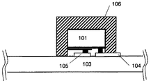
図1は、本発明の第1の実施の形態におけるLED光源のLED部分の断面図を示すものである。図1において、LED101はGaN系LEDであり、発光中心波長が350〜550nmのLEDである。LEDチップの大きさは、約0.3〜2mm角である。約3〜4Vで定格の光出力をする。LEDの定格電流は、発光面の面積に比例し、0.3mm角あたり10〜60mAの電流のものが適当である。本実施の形態のLED101は、発光中心波長が470nm、チップの大きさは、0.3mm角、定格は、3.6Vで20mAであるものを用いた。
(Embodiment 1)
FIG. 1 shows a cross-sectional view of an LED portion of an LED light source in the first embodiment of the present invention. In FIG. 1, an
102はバンプであり、基板103上にある配線パタン104、105とLED101の各電極とを接続している。基板103は、放熱性の高い材料を主材料としており、たとえば、アルミニウム、セラミック、銅などから選択される。なお、本実施の形態の場合は、アルミニウムを主成分としたコンポジット基板を選択した。
A
バンプ102は1つの電極に対して複数の場合もある。本実施の形態の場合は、両電極合計で3個のバンプの場合を選択した。
There may be a plurality of
LED両電極に対応するバンプ間には、樹脂106が存在する。樹脂106は、主成分がシリコーン樹脂であり、TiO2(酸化チタン)、BaTiO3(チタン酸バリウム)などの比誘電率が10以上の材料が含まれている。材料の比誘電率は、実用的には100以上のものが好ましい。また、上記材料は、少なくとも1種樹脂中に10〜70wt%含まれている。なお、本実施の形態の場合は、TiO2が20wt%含まれるものを選択した。本実施の形態の場合、LEDの両極の容量を測定すると、LED単体の容量が数〜30pF程度であったものが、樹脂106を設けることで100pF(1MHz、2V入力時、以下同様の条件で計測)に増加していた。なお、シリコーン樹脂の比誘電率は約3であり、酸化チタンの比誘電率は約100であり、チタン酸バリウムの比誘電率は約1200である。
図2は、図1においてLED101の基板103との接合面を基板側から見たLED101の背面図である。LED101の基板面のバンプ103位置と樹脂106の存在位置を示す。図中の201、202はLEDの電極である。図2中の破線で示した界面とは、N電極201とP電極202とが接触しないように、各電極と絶縁層との界面である。つまり、N電極201に接続されたバンプとP電極202に接続されたバンプ間に樹脂106が存在している。
FIG. 2 is a rear view of the
図3は、LED光源の概観を示したものである。アルミニウム、セラミック、銅などの熱伝導率の高い材料を主成分とした基板103上に、上記LED101が、フリップチップでバンプを介して直接実装されている。ここで、直接実装とは、基板上の配線パタンとLEDがバンプを介して実装されている状態のことを示す。基板上には、図1に示すLED光源が32個直列でかつ2並列構成されており、合計64個のLED101で構成されている。LEDが実装されている範囲は20mm角である。またこの部分の基板面積あたりの実装密度は、16個/cm2である。また、発光部の基板面積あたりの電力は、約1.2W/cm2である。なお、前記実装密度は、1〜100個/cm2程度が用いられる。また、前記基板面積あたりの電力は、0.1〜10W/cm2程度が用いられる。基板103は、大きさが約24×約29mmであり、厚みが約1mmである。厚みのほとんどはアルミニウムでできている。基板上には、給電用の電極端子301がLED実装面と同一面にあり、端子に電圧を印加することでLEDが点灯するようになっている。端子は2並列のため4個ある。32直列してあるLEDのそれぞれについてすべて図1に示す加工が施されている。また、図には示さないが、基板201上の配線パタンは、LEDと接続される部分と端子202の部分以外の表面は、絶縁層で覆われており、外部からの静電気が基板のパタン上に印加されないようになっている。
FIG. 3 shows an overview of the LED light source. The
このようにして、構成されたLED光源の静電破壊試験の内容を以下に説明する。この試験は、静電破壊試験の規格で決められているヒューマンボディーモデル(HBM:人体帯電モデル)の方法に基づいて行った。以下この実験方法について説明する。 The contents of the electrostatic breakdown test of the LED light source thus configured will be described below. This test was performed based on the method of the human body model (HBM: human body charging model) determined by the standard of the electrostatic breakdown test. This experimental method will be described below.
図4に試験装置の回路図を示す。図中の直流電源401の電圧を変化させ、スイッチ402を操作し、2つの端子間を1秒おきに3回往復させる。スイッチをCharge側にすると、電源401の電荷がコンデンサにチャージされ、スイッチ402をDischarge側にするとコンデンサに蓄えられた電荷が抵抗を通って、接続端子間403に接されたLED光源の給電用の電極端子301に電荷が流れる。
FIG. 4 shows a circuit diagram of the test apparatus. The voltage of the
図3のLED光源の2並列のうちの1つの端子301と、図3の端子403を接続し、静電気破壊試験を行った。チェックの方法は、32個の直列に接続されたLEDに定格20mAに対して、1mAの電流を流し、点灯しないLED素子があった場合は、LED素子が破損したものとして判断した。直流電源401の電圧を徐々に高くして、上記実験を繰り返し、LED素子が1つも破損しない最大の電圧(電源401の電圧)を、LED光源の静電耐圧とした。静電気を模擬した電圧を印加した。その後、LEDの損傷状況をチェックした。
One
その結果、電圧の印加する方向が順方向の場合、耐圧は4kV以上、逆方向が4kV以上となることがわかった。ここで、本実施の形態のLED光源は、一般照明など多様な用途に使用されることを考慮し、必要な耐圧は約1kVと考え検討を進めた。この結果より、十分な耐圧を持つ。 As a result, it was found that when the voltage application direction is the forward direction, the withstand voltage is 4 kV or more and the reverse direction is 4 kV or more. Here, considering that the LED light source according to the present embodiment is used for various purposes such as general lighting, the necessary breakdown voltage is about 1 kV, and the examination was advanced. From this result, it has a sufficient breakdown voltage.
これに対して、対策を施していないLED素子の耐圧を測定した。図には示さないが図1に示す本実施の形態のLED光源から樹脂106を抜いたものを同様に静電破壊試験したところ、順方向が4kV以上、逆方向が約600Vとなり、静電耐圧の要求を満たさない。このときLED光源の容量は数〜30pFであり、本実施の形態のLED光源と比べて容量が少ない。
On the other hand, the pressure resistance of the LED element to which no countermeasure was taken was measured. Although not shown in the figure, when the
(実施の形態2)
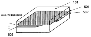
以下、実施の形態2について以下に説明する。実施の形態1と同様の構成で、樹脂106をLED101の周りにコートした場合について説明する。図5に示すようにLEDチップを覆うように樹脂106を厚み0.05〜0.5mmで塗布した。このとき、電極104と樹脂106は接触している。しかし、電極105と樹脂106も接触していないし、電極105上のバンプと樹脂106も接触していない。しかし、本構成の場合、図6に示すように、樹脂106は、LED101側面に露出している各電極層501、502間で接触している。そのため、誘電率の高い樹脂106は電極層501と502間で図10中の503に示すようなコンデンサ成分を持っていると考えられる。
(Embodiment 2)
Hereinafter, Embodiment 2 will be described. A case where the
上記構成のLED光源を実施の形態1と同様に静電破壊試験したところ、順方向が4kV以上、逆方向が約1.2kVとなり、静電耐圧が向上することがわかった。 When the LED light source having the above configuration was subjected to an electrostatic breakdown test in the same manner as in the first embodiment, it was found that the forward direction was 4 kV or more and the reverse direction was about 1.2 kV, and the electrostatic withstand voltage was improved.
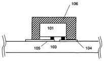
また、図7に示すように基板上の電極105と104のどちらもが樹脂106と接触している場合は、さらに効果的であり、静電耐圧は、順方向4kV以上、逆方向が約1.4kVにまで上昇した。
Further, as shown in FIG. 7, it is more effective when both of the
なお、樹脂厚を0.5mm以上にしても効果は変わらなかった。また、混入する材料をさらに比誘電率の高いチタン酸バリウムでも同様の効果を得ることが出来る。 The effect was not changed even when the resin thickness was 0.5 mm or more. Further, the same effect can be obtained even if the mixed material is barium titanate having a higher relative dielectric constant.
なお、LED101の1個だけの場合の耐圧は、逆方向で200Vである。本実施の形態のLED光源は、LEDが32個直列で接続されているため、理論的には、LED1個あたりの耐圧の32倍の耐圧を示すはずであるが、約3倍程度しか耐圧を持っていない。これは、静電破壊試験は、瞬間的に大きな電圧を印加するため、LEDのもつLもしくはC成分によって、LED32個に均等に電圧がかからずに、1部のLEDに偏って大きな電圧が印加されるためと考えられる。
Note that the withstand voltage in the case of only one
なお、図3に示す光源の発光部全域を上記樹脂で覆えば、より効率的に加工が可能である。 In addition, if the whole light emission part of the light source shown in FIG. 3 is covered with the said resin, it can process more efficiently.
なお、樹脂106は白色系ものを選択し、LEDと基板の間に配置した場合は、有色の基板と比較して光出力が向上するためより好ましい。
In addition, when the
なお、本実施の形態の樹脂106は、シリコーン樹脂を用いたが他の樹脂でもかまわない。ただし、シリコーン樹脂は、他の樹脂に比べると柔らかいので、熱による基板などの膨張に対して歪が小さく信頼性が高くなるという効果がある点、また青色光、紫外光などのエネルギーの高い光でも劣化が少なく寿命中の変化が少ないといった点で好ましい。
In addition, although the
なお、樹脂106に蛍光体を混入して、LEDからの放射光を波長変換してもよい。たとえば、LED101に、青色LEDを用いて、黄色に発光する蛍光体を含む樹脂106とすることで、特に図5、図7の構成の場合、白色光の出力を得ることが出来る。
Note that the
なお、本実施の形態では、比誘電率が3程度のシリコーン樹脂中に、比誘電率の高い材料を混入する方法について記載したが、比誘電率の高い樹脂、例えば比誘電率が3以上(好ましくは5以上)の樹脂を多くすることによって(好ましくは50wt%以上)も、上記と同様に電圧に対する耐性を高めることができる。 In this embodiment, a method of mixing a material having a high relative dielectric constant into a silicone resin having a relative dielectric constant of about 3 is described. However, a resin having a high relative dielectric constant, for example, a relative dielectric constant of 3 or more ( By increasing the amount of resin (preferably 5 or more) (preferably 50 wt% or more), the resistance to voltage can be increased in the same manner as described above.
本発明のLED光源は、静電耐圧が高いLED光源を簡単な構成でえることが出来るので、一般照明などの光源等として有用である。 The LED light source of the present invention can be used as a light source for general illumination because an LED light source having a high electrostatic withstand voltage can be obtained with a simple configuration.
101 LED
102 バンプ
103 基板
104,105,201,202,501,502 電極
106 樹脂
301 電極端子
401 直流電源
402 スイッチ
403 端子
101 LED
102
Claims (4)
両電極間のバンプ間に比誘電率が10以上の材料を5wt%以上含む樹脂が配置されている、LED光源。 An LED light source in which a GaN-based LED electrode and a wiring pattern on a substrate are flip-chip mounted by bumps,
An LED light source in which a resin containing 5 wt% or more of a material having a relative dielectric constant of 10 or more is disposed between bumps between both electrodes.
LEDチップ周囲は、比誘電率が10以上の材料を5wt%以上含む樹脂で覆われており、前記樹脂はLEDチップ側面のP型電極層およびN型電極層のどちらとも接触している、LED光源。 An LED light source in which a GaN-based LED electrode and a wiring pattern on a substrate are flip-chip mounted by bumps,
The periphery of the LED chip is covered with a resin containing 5 wt% or more of a material having a relative dielectric constant of 10 or more, and the resin is in contact with both the P-type electrode layer and the N-type electrode layer on the side surface of the LED chip. light source.
LEDチップの周囲は、比誘電率が10以上の材料を5wt%以上含む樹脂で覆われており、前記樹脂はLEDチップの両電極とも接触している、LED光源。 An LED light source in which a GaN-based LED electrode and a wiring pattern on a substrate are flip-chip mounted by bumps,
An LED light source in which the periphery of an LED chip is covered with a resin containing 5 wt% or more of a material having a relative dielectric constant of 10 or more, and the resin is in contact with both electrodes of the LED chip.
Priority Applications (1)
| Application Number | Priority Date | Filing Date | Title |
|---|---|---|---|
| JP2004111791A JP2005294779A (en) | 2004-04-06 | 2004-04-06 | LED light source |
Applications Claiming Priority (1)
| Application Number | Priority Date | Filing Date | Title |
|---|---|---|---|
| JP2004111791A JP2005294779A (en) | 2004-04-06 | 2004-04-06 | LED light source |
Publications (1)
| Publication Number | Publication Date |
|---|---|
| JP2005294779A true JP2005294779A (en) | 2005-10-20 |
Family
ID=35327330
Family Applications (1)
| Application Number | Title | Priority Date | Filing Date |
|---|---|---|---|
| JP2004111791A Pending JP2005294779A (en) | 2004-04-06 | 2004-04-06 | LED light source |
Country Status (1)
| Country | Link |
|---|---|
| JP (1) | JP2005294779A (en) |
Cited By (4)
| Publication number | Priority date | Publication date | Assignee | Title |
|---|---|---|---|---|
| KR100964370B1 (en) | 2008-04-10 | 2010-06-25 | 조인셋 주식회사 | LED chip package with instantaneous high voltage protection |
| KR101423929B1 (en) * | 2007-12-26 | 2014-08-04 | 삼성전자주식회사 | Light Emitting Diode device |
| JP2015028188A (en) * | 2014-11-10 | 2015-02-12 | 株式会社朝日ラバー | Silicone resin base material |
| WO2019003775A1 (en) * | 2017-06-29 | 2019-01-03 | 京セラ株式会社 | Circuit board and light-emitting device provided with same |
-
2004
- 2004-04-06 JP JP2004111791A patent/JP2005294779A/en active Pending
Cited By (7)
| Publication number | Priority date | Publication date | Assignee | Title |
|---|---|---|---|---|
| KR101423929B1 (en) * | 2007-12-26 | 2014-08-04 | 삼성전자주식회사 | Light Emitting Diode device |
| KR100964370B1 (en) | 2008-04-10 | 2010-06-25 | 조인셋 주식회사 | LED chip package with instantaneous high voltage protection |
| JP2015028188A (en) * | 2014-11-10 | 2015-02-12 | 株式会社朝日ラバー | Silicone resin base material |
| WO2019003775A1 (en) * | 2017-06-29 | 2019-01-03 | 京セラ株式会社 | Circuit board and light-emitting device provided with same |
| CN110800118A (en) * | 2017-06-29 | 2020-02-14 | 京瓷株式会社 | Circuit board and light-emitting device provided with same |
| JPWO2019003775A1 (en) * | 2017-06-29 | 2020-04-02 | 京セラ株式会社 | Circuit board and light emitting device including the same |
| CN110800118B (en) * | 2017-06-29 | 2022-10-28 | 京瓷株式会社 | Circuit board and light-emitting device provided with same |
Similar Documents
| Publication | Publication Date | Title |
|---|---|---|
| CN105428385B (en) | Light sources utilizing segmented LEDs to compensate for manufacturing process variations in light output of individual segmented LEDs | |
| US7544524B2 (en) | Alternating current light-emitting device | |
| US7531843B2 (en) | Structure of AC light-emitting diode dies | |
| US8390021B2 (en) | Semiconductor light-emitting device, light-emitting module, and illumination device | |
| US7675087B1 (en) | Surface mount light emitting device | |
| JP2011146353A (en) | Lighting apparatus | |
| US20110089443A1 (en) | Packaging Structure of AC light-emitting diodes | |
| JP5655302B2 (en) | Lighting device | |
| JP2005276979A (en) | LED light source | |
| CN108140696A (en) | Micro wire containing temperature measuring equipment or nanowire LED light source | |
| JP2004014899A (en) | Series structure of light emitting diode chips | |
| CN104081548A (en) | Light emission device and illumination device | |
| US20110199021A1 (en) | Light-emitting device and lighting apparatus provided with the same | |
| JP5516956B2 (en) | Light emitting device and lighting device | |
| TWI398971B (en) | Light emitting diode package structure | |
| JPWO2009104645A1 (en) | Lighting equipment | |
| JP6939740B2 (en) | Semiconductor module | |
| JP2005294779A (en) | LED light source | |
| TWI428536B (en) | LED light bar | |
| TWM310457U (en) | Light emitting diode module and apparatus thereof | |
| JP2020061325A (en) | Light emitting device with power generation function, lighting device, and display device | |
| JP2005303174A (en) | LED light source | |
| JP2012094661A (en) | Light-emitting device and lighting device | |
| JP2005303175A (en) | LED light source | |
| US8633639B2 (en) | Multichip package structure and light bulb of using the same |