JP2005294776A - Position detecting apparatus and position detecting method - Google Patents
Position detecting apparatus and position detecting method Download PDFInfo
- Publication number
- JP2005294776A JP2005294776A JP2004111753A JP2004111753A JP2005294776A JP 2005294776 A JP2005294776 A JP 2005294776A JP 2004111753 A JP2004111753 A JP 2004111753A JP 2004111753 A JP2004111753 A JP 2004111753A JP 2005294776 A JP2005294776 A JP 2005294776A
- Authority
- JP
- Japan
- Prior art keywords
- alignment
- value
- dimensional shape
- signal waveform
- mark
- Prior art date
- Legal status (The legal status is an assumption and is not a legal conclusion. Google has not performed a legal analysis and makes no representation as to the accuracy of the status listed.)
- Withdrawn
Links
Images


Landscapes
- Length Measuring Devices By Optical Means (AREA)
- Exposure And Positioning Against Photoresist Photosensitive Materials (AREA)
- Exposure Of Semiconductors, Excluding Electron Or Ion Beam Exposure (AREA)
Abstract
【課題】 正確な位置合わせを可能とする位置合わせ方法とそれを用いた露光装置と、それに好適なオフセット計測装置を提供する。
【解決手段】 ウエハ上のマークの位置検出装置において、マークのレジスト塗布前後の各立体形状の測定データを用いて、シミュレータによりレジスト塗布後のアライメント信号波形を計算により求め、該計算により求めたアライメント信号波形を用いてレジスト塗布後のアライメント値のオフセットを求める時、レジスト塗布前後のマークの立体形状の相対位置をアライメントスコープを用いて得られたアライメント検出値と合致させる為に、レジスト塗布前のマークの立体形状とレジスト塗布後のマークの立体形状の該相対位置を調整してシミュレータにより計算する。
【選択図】 図9
PROBLEM TO BE SOLVED: To provide an alignment method capable of accurate alignment, an exposure apparatus using the alignment method, and an offset measuring apparatus suitable for the alignment method.
In a mark position detection apparatus on a wafer, an alignment signal waveform after resist application is obtained by calculation using a simulator using measurement data of each three-dimensional shape before and after resist application of the mark, and the alignment obtained by the calculation is obtained. When calculating the offset of the alignment value after resist application using the signal waveform, in order to match the relative position of the three-dimensional shape of the mark before and after resist application with the alignment detection value obtained using the alignment scope, The relative position of the three-dimensional shape of the mark and the three-dimensional shape of the mark after application of the resist is adjusted and calculated by the simulator.
[Selection] Figure 9
Description
本発明は、例えば半導体製造用の露光装置において、第1物体としてのレチクル面上に形成されているIC、LSI、VLSI等の微細な電子回路パターンと、第2物体としてのウエハとの相対的な位置合わせ(アライメント)をおこなう為の位置合わせ方法及び露光装置に関するものである。また本発明は、特にウエハプロセス誤差であるWIS(Wafer Induced Shift)が発生しうる状況においてアライメントをおこなう必要がある位置合わせ方法及び露光装置に関するものである。 For example, in an exposure apparatus for manufacturing a semiconductor, the present invention relates to a relative relationship between a fine electronic circuit pattern such as an IC, LSI, VLSI or the like formed on a reticle surface as a first object and a wafer as a second object. The present invention relates to an alignment method and an exposure apparatus for performing accurate alignment. The present invention also relates to an alignment method and an exposure apparatus that require alignment in a situation where WIS (Wafer Induced Shift), which is a wafer process error, can occur.
半導体製造用の投影露光装置には、集積回路の高密度化に伴いレチクル面上の回路パターンをウエハ面上に、より高い解像力で投影露光することが要求されている。回路パターンの投影解像力を向上させる手段としては、露光光の波長を固定して投影光学系のNAを大きくしたり、露光光をより短波長化して露光する方法がとられている。 2. Description of the Related Art A projection exposure apparatus for semiconductor manufacturing is required to project and expose a circuit pattern on a reticle surface onto a wafer surface with higher resolution as the integrated circuit has a higher density. As means for improving the projection resolving power of the circuit pattern, a method is adopted in which the exposure light wavelength is fixed to increase the NA of the projection optical system, or the exposure light is made to have a shorter wavelength for exposure.
一方、回路パターンの微細化に伴い電子回路パターンが形成されているレチクルとウエハとの高精度アライメントに対する要求もますます厳しくなっている。 On the other hand, with the miniaturization of circuit patterns, the demand for high-precision alignment between a reticle on which an electronic circuit pattern is formed and a wafer is becoming stricter.
レチクルとウエハの位置合わせには、ウエハ面上に塗布されたレジストを感光させる露光光を使用する場合と、感光させない非露光光、例えばHe−Neレーザの発振波長である633nm を使用する場合があるが、現状の実用化されているアライメントの使用波長は、非露光光がほとんどである。これは非露光光が半導体製造プロセスの影響を受けにくいことが大きな理由であり、特にレジストに対する透過率が高い為、ウエハマークをレジスト特性に関係なく観察できるというメリットを持っているためである。 For alignment between the reticle and the wafer, there are a case where exposure light for exposing the resist coated on the wafer surface is used and a case where non-exposure light that is not exposed, for example, 633 nm which is the oscillation wavelength of a He—Ne laser is used. However, most of the wavelengths used for the alignment that are currently in practical use are non-exposure light. This is mainly because the non-exposure light is not easily affected by the semiconductor manufacturing process. In particular, since the transmittance with respect to the resist is high, the wafer mark can be observed regardless of the resist characteristics.
非露光光を用いた位置合わせ装置の出願が、例えば特許文献1や特許文献2等で提案され、実際に製品化されて効果が確認されている。
An application for an alignment apparatus using non-exposure light has been proposed in, for example, Patent Document 1 and
前記、従来公知のアライメント技術は非露光光TTL(Through The Lens)Off−axis方式と呼ばれ、レチクルパターンをウエハ上に転写投影する投影光学系に非露光光を通したとき発生する色収差をアライメント光学系で補正している。 The conventionally known alignment technique is called non-exposure light TTL (Through The Lens) Off-axis method, and aligns chromatic aberration generated when non-exposure light is passed through a projection optical system for transferring and projecting a reticle pattern onto a wafer. Corrected by optical system.
また、現在実際に使用されているアライメント方法のほとんどは、ウエハ上のアライメントマークの光学像をCCD カメラ等の撮像素子上に結像して得られる電気信号を画像処理し、ウエハ位置を検出する方法が採用されている。ここで画像処理とは特許文献3等で紹介されている対称性マッチング法、あるいはテンプレートマッチング法等を用いてもよい。 In addition, most of the alignment methods that are actually used at present detect the wafer position by performing image processing on an electrical signal obtained by forming an optical image of the alignment mark on the wafer on an image sensor such as a CCD camera. The method is adopted. Here, as the image processing, a symmetry matching method or a template matching method introduced in Patent Document 3 or the like may be used.
前述の画像処理を使用した非露光光TTL Off−axis方式はi線ステッパ−には使用されているが、エキシマレーザを光源とするエキシマステッパ−には採用されていない。理由は、エキシマステッパ−の投影光学系の場合、非露光光、例えばHe−Neレーザの発振波長である633nmで発生する投影光学系の色収差が非常に大きく、アライメント光学系での補正を高NAでおこなうことができないからである。 The non-exposure light TTL Off-axis method using the image processing described above is used for an i-line stepper, but is not used for an excimer stepper using an excimer laser as a light source. The reason is that in the case of the excimer stepper projection optical system, non-exposure light, for example, the chromatic aberration of the projection optical system generated at 633 nm, which is the oscillation wavelength of the He-Ne laser, is very large, and correction in the alignment optical system can This is because it cannot be done.
このためエキシマステッパ−においては、前述の非露光光TTL Off−axis方式に代わり、投影光学系を通さないOff−axis顕微鏡を設け、非露光波長で観察をおこなう非露光光Off−axis方式の画像処理方式の検出系がほとんどである。 Therefore, in the excimer stepper, in place of the above-described non-exposure light TTL Off-axis method, an off-axis microscope that does not pass through the projection optical system is provided, and an image of the non-exposure light Off-axis method that performs observation at a non-exposure wavelength. Most detection systems are processing methods.
非露光光Off−axis方式は投影光学系を通らない方式、即ちTTLではなくnon TTL Off−axis方式であるため、Off−axis顕微鏡と投影光学系との距離、いわゆるベースラインの変動が精度劣化の要因となる。ベースラインの変動を抑え、高精度アライメントを達成するため、非露光光Off−axis方式では熱的に影響されにくい部材を使用したり、頻繁にベースライン補正をおこなうことが必要とされる。 Since the non-exposure light off-axis method is a method that does not pass through the projection optical system, that is, a non-TTL off-axis method, not TTL, the accuracy of the distance between the off-axis microscope and the projection optical system, that is, the so-called baseline fluctuation It becomes a factor of. In order to suppress baseline fluctuation and achieve high-precision alignment, the non-exposure light off-axis method requires the use of a member that is not easily affected by heat, and frequent baseline correction.
また、エキシマステッパーにおける非露光光TTL Off−axis方式では、画像処理方式以外のものも採用されている。画像処理以外の方式とはアライメントマークからの直接反射光を検出せず、限られた回折光の光のみ使用する暗視野検出方式であり、ヘテロダイン検出と呼ばれる方式も当てはまる。 Further, in the excimer stepper, the non-exposure light TTL Off-axis method employs other than the image processing method. A method other than image processing is a dark field detection method that does not detect directly reflected light from the alignment mark but uses only limited diffracted light, and a method called heterodyne detection is also applicable.
限られた回折光を検出する非露光光TTL Off−axis方式は既に提案されている。この方式はベースラインが短い為、TTLでない非露光光Off−axis方式の欠点は解消しているが、暗視野検出の為、明視野検出に比較すると検出率に問題が存在する。 A non-exposure light TTL Off-axis method for detecting limited diffracted light has already been proposed. Since this method has a short base line, the disadvantage of the non-exposure light off-axis method that is not TTL is solved. However, there is a problem in detection rate compared with bright field detection because of dark field detection.
現状の製造においては、上記の画像処理方式、画像処理方式以外の検出方式それぞれの短所、長所をプロセスに応じて見極めて選択し、使用する事で、要求される高精度の位置合わせを可能としている。 In the current manufacturing, the disadvantages and advantages of each of the above image processing methods and detection methods other than the image processing method are determined and used according to the process, enabling the required high-precision alignment. Yes.
しかしながら、現在要求されているアライメントのさらなる高精度の要求に対しては、前述の二方式を用いても、半導体プロセスの誤差に対してまだ解決されない問題が存在する。最も大きな問題は、プロセスによりアライメントマーク形状が非対称になる事に対する対応がなされていない点である。 However, there is a problem that is still unresolved with respect to errors in the semiconductor process even if the above-described two methods are used for the demand for higher accuracy of alignment currently required. The biggest problem is that no measures are taken against the fact that the alignment mark shape becomes asymmetric due to the process.
一例としてはメタルCMP(Chemical Mechanical Polishing)工程等における平坦化プロセスを挙げることができる。該CMP工程ではアライメントマークの構造が非対称となり、グローバルアライメントにおいて、回転エラーや、倍率エラーが発生し、精度が低下することが大きなが問題となっている。平坦化プロセスによるウエハのアライメントマークの構造の歪は、暗視野検出方式に誤差として大きく発生しやすく、精度低下の原因となる。従ってベースラインの安定性を画像処理方式以外の非露光光TTL Off−axis方式で達成しても、プロセス敏感度が高いことで、実際には使用されているケースが少ないのが現実である。 As an example, a planarization process in a metal CMP (Chemical Mechanical Polishing) process or the like can be given. In the CMP process, the structure of the alignment mark becomes asymmetric, and in the global alignment, a rotation error and a magnification error occur, and the accuracy is seriously lowered. The distortion of the structure of the alignment mark on the wafer due to the flattening process is likely to occur as a large error in the dark field detection method, causing a reduction in accuracy. Therefore, even if the stability of the baseline is achieved by the non-exposure light TTL Off-axis method other than the image processing method, the fact is that there are few cases where it is actually used due to the high process sensitivity.
このプロセスによるアライメントマーク形状の非対称化したことによるアライメントオフセット値の検出を、プロファイラ−と光学シミュレータ(以下、シミュレータと呼ぶ)を用いることによりおこなうオフセットアナライザーと呼ぶ装置を用いた補正方法が、特許文献4として本出願人が提案しており、効果が確認されている。
しかしながら、特許文献4においては、プロファイラ−で測定したアライメントマークの立体形状を用いて、アライメント信号波形を計算する際の、レジスト塗布前後におけるアライメントマークの立体形状の相対位置関係の決定は、アライメントスコープで得られたアライメント信号波形とシミュレータにより得られたアライメント信号波形の形状を一致させる方法が述べられているが、この方法では概略の相対位置決めはできるが、詳細な位置決めはできない方法であった。本発明は、上述従来例に鑑み、より正確な位置合わせを可能とする位置合わせ方法とそれを用いた露光装置と、それに好適なオフセット計測装置を提供することを目的とする。
However, in
本発明は、ウエハ上のアライメントマークの位置検出装置において、ウエハ上のアライメントマークのレジスト塗布前後の各立体形状の測定データを用いて、シミュレータによりレジスト塗布後のアライメント信号波形を計算により求め、該計算により求めたアライメント信号波形を用いてレジスト塗布後のアライメント値のオフセットを求める時、
前記レジスト塗布後のアライメント信号波形を計算により求める際、
レジスト塗布前のアライメントマークの立体形状と、
レジスト塗布後のアライメントマークの立体形状、
の相対位置を、
アライメントスコープを用いて得られたアライメント検出値と合致させる為に、レジスト塗布前のアライメントマークの立体形状とレジスト塗布後のアライメントマークの立体形状の該相対位置を調整してシミュレータにより計算する時、該相対位置を以下のようにして決定する。
In the alignment mark position detection apparatus on the wafer, the alignment signal waveform after resist application is calculated by a simulator using a measurement data of each three-dimensional shape before and after resist application of the alignment mark on the wafer. When calculating the offset of the alignment value after resist application using the alignment signal waveform obtained by calculation,
When obtaining the alignment signal waveform after the resist coating by calculation,
Three-dimensional shape of alignment mark before resist application,
Three-dimensional shape of alignment mark after resist application,
Relative position of
In order to match with the alignment detection value obtained using the alignment scope, when calculating the relative position of the three-dimensional shape of the alignment mark before resist coating and the three-dimensional shape of the alignment mark after resist coating and calculating by the simulator, The relative position is determined as follows.
1.ライメントスコープを用いて、ウエハ上のアライメントマークに対するアライメント値を検出する。 1. An alignment value with respect to the alignment mark on the wafer is detected by using the alignment scope.
2.該アライメントスコープによるアライメント値の検出は、少なくとも2つ以上の照明光を用いておこない、第1の波長を有する照明光と第2の波長を有する照明光を順次アライメントマークに照射し、各波長の照明光を照射した状態毎に、アライメントスコープを用いて少なくとも2つのアライメント値を求め、該少なくとも2つのアライメント値間の差分を計算し、第1の差分値を求める。 2. The alignment value is detected by the alignment scope using at least two or more illumination lights, the illumination light having the first wavelength and the illumination light having the second wavelength are sequentially irradiated to the alignment mark, For each state irradiated with illumination light, at least two alignment values are obtained using an alignment scope, a difference between the at least two alignment values is calculated, and a first difference value is obtained.
3.レジスト塗布前後で測定した前記アライメントマークの立体形状を合成して、該合成した立体形状を用いて、シミュレータによりアライメント値を計算する。 3. A three-dimensional shape of the alignment mark measured before and after resist application is synthesized, and an alignment value is calculated by a simulator using the synthesized three-dimensional shape.
4.該合成した立体形状を、該相対位置のずれ量が異なる状態の物を少なくとも2つ以上用意する。 4). At least two or more of the synthesized three-dimensional shapes are prepared in different states of the relative position shift amount.
5.該合成した立体形状のうち、第1の立体形状に対して、該第1の波長を有する照明光と該第2の波長を有する照明光の状態をシミュレータ内に設定し、各照明状態毎にアライメント値を計算し、少なくとも2つのアライメント値間の差分を計算し、第2の差分値を求める。 5). Among the synthesized three-dimensional shapes, the state of the illumination light having the first wavelength and the illumination light having the second wavelength is set in the simulator with respect to the first three-dimensional shape. An alignment value is calculated, a difference between at least two alignment values is calculated, and a second difference value is obtained.
6.該合成した立体形状のうち、第2の立体形状に対して、該第1の波長を有する照明光と該第2の波長を有する照明光の状態をシミュレータ内に設定し、各照明状態毎にアライメント値を計算し、少なくとも2つのアライメント値間の差分を計算し、第3の差分値を求める。 6). Among the synthesized three-dimensional shapes, the illumination light having the first wavelength and the illumination light having the second wavelength are set in the simulator with respect to the second three-dimensional shape. An alignment value is calculated, a difference between at least two alignment values is calculated, and a third difference value is obtained.
7.該第1の差分値と、該第2の差分値、該第3の差分値を比較し、該アライメントスコープから得られた差分値に対し、シミュレータから得られる差分値が同等になる合成状態である立体形状を求め、該相対位置を決定する。
ことを特徴としている。
7). The first difference value is compared with the second difference value and the third difference value, and the difference value obtained from the simulator is equivalent to the difference value obtained from the alignment scope. A certain three-dimensional shape is obtained and the relative position is determined.
It is characterized by that.
また、該少なくとも2つ以上のアライメント照明光において、各照明光の波長は単一波長からなる光であり、各照明光の波長は互いに異なることを特徴としている。 Further, in the at least two or more alignment illumination lights, the wavelength of each illumination light is a light having a single wavelength, and the wavelengths of each illumination light are different from each other.
また、該少なくとも2つ以上のアライメント照明光において、少なくとも1つはブロードバンドの波長領域を有する照明光であり、その他の照明光は、単一波長を有する照明光であることを特徴としている。 Further, at least one of the at least two alignment illumination lights is illumination light having a broadband wavelength region, and the other illumination light is illumination light having a single wavelength.
また、該少なくとも2つ以上のアライメント照明光毎にアライメント信号波形を求め、各計算により求めたアライメント信号波形からアライメント値を求める際、アライメント値を測定する時のアライメント検出光学系の照明系のコヒーレンシの値が互いに異なることを特徴としている。 Further, when the alignment signal waveform is obtained for each of the at least two alignment illumination lights and the alignment value is obtained from the alignment signal waveform obtained by each calculation, the coherency of the illumination system of the alignment detection optical system when measuring the alignment value is obtained. The values of are different from each other.
また、該少なくとも2つ以上のアライメント照明光毎にアライメント信号波形を求め、各計算により求めたアライメント信号波形からアライメント値を求める際、アライメント値を測定する時のアライメント検出光学系に対するアライメントマークのフォーカス位置が互いに異なることを特徴としている。 In addition, when the alignment signal waveform is obtained for each of the at least two alignment illumination lights, and the alignment value is obtained from the alignment signal waveform obtained by each calculation, the alignment mark is focused on the alignment detection optical system when measuring the alignment value. The positions are different from each other.
また、該少なくとも2つ以上のアライメント照明光毎にアライメント信号波形を求め、各計算により求めたアライメント信号波形からアライメント値を求める際、アライメント値を測定する時のアライメント検出光学系の開口数(NA)が互いに異なることを特徴としている。 Further, when obtaining an alignment signal waveform for each of the at least two alignment illumination lights and obtaining an alignment value from the alignment signal waveform obtained by each calculation, the numerical aperture (NA) of the alignment detection optical system when measuring the alignment value is obtained. ) Are different from each other.
また、該少なくとも2つ以上のアライメント照明光毎にアライメント信号波形を求め、各計算により求めたアライメント信号波形からアライメント値を求める際、アライメント値を測定する時のアライメント検出光学系の照明系の偏光条件が互いに異なることを特徴としている。 Further, when the alignment signal waveform is obtained for each of the at least two alignment illumination lights and the alignment value is obtained from the alignment signal waveform obtained by each calculation, the polarization of the illumination system of the alignment detection optical system when measuring the alignment value It is characterized by different conditions.
また、該計算により求めたアライメント信号波形から、ウエハプロセス要因で生じるアライメントオフセットを求めて、アライメントスコープによるアライメント検出の際、前記アライメントオフセットを考慮しアライメントをおこなうことを特徴としている。 Further, an alignment offset caused by a wafer process factor is obtained from an alignment signal waveform obtained by the calculation, and alignment is performed in consideration of the alignment offset when detecting an alignment by an alignment scope.
本発明によれば、ウエハプロセスによるウエハ上のアライメントマークの立体形状の変化によって生じるアライメントオフセットエラーを、プロファイラーとシミュレータにより求める時、プロファイラーによるレジスト塗布前後のアライメントマークの立体形状測定値の相対位置決めを精度よくおこなうことが可能となる。 According to the present invention, when the alignment offset error caused by the change in the three-dimensional shape of the alignment mark on the wafer due to the wafer process is obtained by the profiler and the simulator, the profiler measures the relative positioning of the three-dimensional shape measurement value of the alignment mark before and after resist application. It is possible to perform with high accuracy.
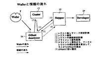
先ず、本発明の第1の実施形態を説明する。図5はオフセットアナライザー、位置合わせ装置を有する露光装置、及び周辺装置における、ウエハと各装置で得られる情報の流れを示した図である。なお、オフセットアナライザーは特許文献4にも紹介されているが、実施例の説明を容易に進める為、オフセットアナライザーの構成、及び測定原理を記載しながら説明を進める。また、以下の説明では露光装置をステッパー、露光装置に搭載されている位置合わせ装置の位置合わせ検出系をアライメントスコープと呼ぶ。また、オフセットアナライザーの構成エレメントの一つである、アライメントマークの立体形状を測定する測定装置は、光学方式を採用した測定器を用いることができるが、特許公報2735632号公報に示されている走査型トンネル顕微鏡や、特開平5−217861号公報に示されている原子間力顕微鏡(Atomic Force Microscope:AFM)等の分解能の高い方式を用いることもできる。本発明の実施形態では、アライメントマークの立体形状の検出には、AFMを用いた形態を代表として記述する。
First, a first embodiment of the present invention will be described. FIG. 5 is a diagram showing the flow of information obtained by the wafer and each apparatus in the offset analyzer, the exposure apparatus having the alignment apparatus, and the peripheral apparatus. Although the offset analyzer is also introduced in
図5において、ウエハWはまず工程(1)で示す様に、レジストを塗布する前にオフセットアナライザーOAに運ばれ、レジスト塗布前のアライメントマークの立体形状をAFMで測定する。 In FIG. 5, the wafer W is first transported to the offset analyzer OA before applying the resist as shown in step (1), and the three-dimensional shape of the alignment mark before applying the resist is measured by AFM.
次に工程(2)でウエハWはコーターCTに運ばれてレジストが塗布され、工程(3)で再度オフセットアナライザーOAに運ばれてアライメントマーク上のレジストの立体形状をAFMで測定する。 Next, in step (2), the wafer W is transported to the coater CT and applied with a resist, and in step (3), it is transported again to the offset analyzer OA, and the three-dimensional shape of the resist on the alignment mark is measured by AFM.
ウエハWは次に工程(4)でステッパ−STに運ばれてアライメントスコープによりアライメントマークの信号が検出され、工程(5)でステッパ−STからアライメントマークの信号情報をオフセットアナライザーOAに送る。 The wafer W is then transferred to the stepper ST in step (4), and an alignment mark signal is detected by the alignment scope. In step (5), the alignment mark signal information is sent from the stepper ST to the offset analyzer OA.
続く工程(6)では、予めオフセットアナライザーOAでレジスト塗布前後で求めたレジストとウエハマークとの3次元的な相対位置関係より、アライメントスコープにより得られたアライメントマーク信号とウエハマーク位置との関係を求めてアライメント計測のオフセットを算出し、ステッパ−STに送る。ステッパ−STでは送られてきたオフセットをもとにグローバルアライメントをおこない、その後、露光をおこない、全てのショットの露光終了後、ウエハWは現像のためデベロッパーDVへ搬送される。現像後、いくつかの処理を経て回路を形成し、最終的に半導体デバイスが製造される。 In the following step (6), the relationship between the alignment mark signal obtained by the alignment scope and the wafer mark position is obtained from the three-dimensional relative positional relationship between the resist and the wafer mark obtained before and after applying the resist by the offset analyzer OA. The offset of alignment measurement is calculated and sent to the stepper ST. The stepper ST performs global alignment based on the offset sent, and then performs exposure. After exposure of all shots is completed, the wafer W is transferred to the developer DV for development. After development, a circuit is formed through several processes, and finally a semiconductor device is manufactured.
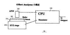
図6はオフセットアナライザーの構成を示したものである。 FIG. 6 shows the configuration of the offset analyzer.
オフセットアナライザーは、ウエハWを支持するチャック101、前記チャック101を三次元的に移動させるXYZステージ102、レジスト塗布前/塗布後の状態でのアライメントマークの立体形状を計測するAFM103、オフセットアナライザー全体を制御し、かつ検出された立体形状からアライメントオフセットを算出するシミュレータを有したCPU104から構成されている。なお、図6ではウエハ搬送系やウエハの三次元位置検出系は不図示となっている。
The offset analyzer includes a chuck 101 that supports the wafer W, an
次に、図1〜図4、図8〜図9を用いて、オフセットアナライザーでおこなわれている、工程(1)(図5)のレジスト無しでのマーク形状計測と、工程(3)(図5)のレジストの表面形状計測のデータからアライメント信号波形をシミュレータにより求め、その信号波形から、レジスト塗布後のアライメント値の変化量を求める過程を説明する。以下に説明する過程は、図9に示す流れ図に従っているものとする。 Next, using FIG. 1 to FIG. 4 and FIG. 8 to FIG. 9, mark shape measurement without a resist in step (1) (FIG. 5), which is performed by an offset analyzer, and step (3) (FIG. The process of obtaining the alignment signal waveform from the resist surface shape measurement data of 5) using a simulator and obtaining the change amount of the alignment value after resist application from the signal waveform will be described. Assume that the process described below follows the flowchart shown in FIG.
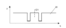
図2(a)は、ウエハW上のアライメントマークの概略図であり、図2(b)は、図2(a)のアライメントマークの断面図である。図2(a)の破線で囲った部分のマークの立体形状をAFMで先ず測定をする(工程7)。その立体形状20の測定結果の概略を図3に示す。ここで、図3の結果を基に、シミュレータにより、レジスト塗布前のアライメント信号波形を計算により求め、その波形に対して画像処理をおこない、レジスト塗布前のアライメントマークから得られるシミュレータによるアライメント値A1を求める(工程8)。
2A is a schematic view of the alignment mark on the wafer W, and FIG. 2B is a cross-sectional view of the alignment mark in FIG. First, the three-dimensional shape of the mark surrounded by the broken line in FIG. 2A is first measured by AFM (step 7). The outline of the measurement result of the three-
本発明で述べるシミュレータとは、Maxwell方程式を時間と空間について差分化し、その差分方程式を領域内の電磁場が安定するまで、磁界と電界について交互に計算する時間領域差分法(FDTD法)を用いたTEMPESTにより、アライメントマーク近傍でのアライメント信号光の位相と振幅値を計算し、これらの値を、EM−Series(光学像計算プログラム)、CODE V(光学設計、評価プログラム)等の市販ソフトウエアに取り込み、検出面上でのアライメント信号波形を計算するものである。 The simulator described in the present invention uses a time-domain difference method (FDTD method) in which the Maxwell equation is differentiated with respect to time and space, and the difference equation is alternately calculated for a magnetic field and an electric field until the electromagnetic field in the region is stabilized. TEMPEST calculates the phase and amplitude values of the alignment signal light near the alignment mark, and these values are used for commercial software such as EM-Series (optical image calculation program) and CODE V (optical design and evaluation program). The alignment signal waveform on the capture and detection surface is calculated.
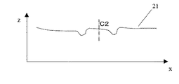
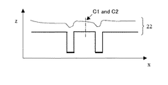
次に、レジスト塗布後のアライメントマークの立体形状21を図4に示す(工程9)。そしてレジスト塗布前のアライメントマークの立体形状(図3)とレジスト塗布後のアライメントマークの立体形状(図4)を合成し(工程10)、この合成した立体形状22に対してシミュレータを用いてアライメント信号波形を計算し、レジストが塗布されている状態でのアライメントマークから得られるアライメント信号波形として、その波形からアライメント値A2を求める(工程11)。そして、A1とA2の差を取ることにより、レジスト塗布によるアライメント値の変化(=WIS)の値を求めることができる(工程12)。
Next, the three-
しかし、前述の図3と図4に示す立体形状20、21の合成時(図9の工程10)に、その合成後の立体形状22が、現実のウエハ上での形状と同等でなければ、得られる波形、及びその波形から得られるアライメント値は正しい値は示さない。以下、本出願で提案する、AFMで測定したレジスト塗布前後の立体形状20、21の合成を、現実のウエハ上での形状と同等の状態で重ね合わせる方法を述べる。
However, when the three-
図10は、図9の工程10の部分を更に詳細に説明する図であり、AFMで測定したレジスト塗布前後の立体形状20、21の合成方法を示す流れ図である。
FIG. 10 is a diagram for explaining the part of
先ず、レジスト塗布前後で、AFMで測定したアライメントマークを有するウエハWは、ステッパ−に送られ、ステッパ−内のアライメントスコープを用いてアライメント信号が検出され、検出されたアライメント信号に対して画像処理検出をおこない、アライメント値が算出される。 First, the wafer W having alignment marks measured by AFM before and after resist coating is sent to a stepper, an alignment signal is detected using an alignment scope in the stepper, and image processing is performed on the detected alignment signal. Detection is performed and an alignment value is calculated.
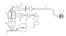
図7はアライメントスコープの構成を示す図であり、光源が、ハロゲンランプ5以外に複数用意されており(不図示)、光源からの光はファイバー7に導かれている。ファイバー7から出た光は、照明光学系8、ビームスプリッタ−9、及びレンズ10を通過し、ウエハ1上のアライメントマーク3を明視野照明する。アライメントマークからのアライメント信号光は、レンズ10、ビームスプリッタ9、結像光学系11、12を通り、CCD13の撮像面上に結像され、CCD13から得られた画像信号に対してアライメント値を求める。また、不図示のアパーチャの大きさ(開口の直径)を変えることにより、照明光学系のNAと、検像光学系のNAの比率(=σ)を変えて、アライメント信号波形の検出をおこなってもよい。
FIG. 7 is a diagram showing the configuration of the alignment scope. A plurality of light sources other than the halogen lamp 5 are prepared (not shown), and light from the light sources is guided to the fiber 7. The light emitted from the fiber 7 passes through the illumination
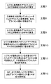
アライメント信号の検出は、アライメントマークに対する照明光の波長を少なくとも2つ設定して、設定したアライメント波長毎にアライメント信号を検出し、アライメント値を算出する(工程13)。ここでは、例えば照明光の波長をλ1=554nm、λ2=626nmと設定し、各波長毎に検出したアライメント値を、それぞれXλ1、Xλ2とし、その差分をΔX1=Xλ1−Xλ2とし、ΔX1の値をCPU104に記憶する(工程14)。 In the detection of the alignment signal, at least two wavelengths of illumination light for the alignment mark are set, the alignment signal is detected for each set alignment wavelength, and an alignment value is calculated (step 13). Here, for example, the wavelength of the illumination light is set as λ1 = 554 nm and λ2 = 626 nm, the alignment values detected for each wavelength are X λ1 and X λ2 , respectively, and the difference is ΔX1 = X λ1 −X λ2 , The value of ΔX1 is stored in the CPU 104 (step 14).
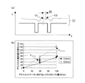
次に、図3、図4に示す立体形状20、21を合成し、合成した立体形状を基にシミュレータを用いて計算によりアライメント信号を求める。まず、図3、図4で表される立体形状を、図8に示すように、例えば個々の立体形状の重心位置が一致するように合成する(工程15)。この状態での立体形状20、21互いの相対位置ずれ量Sfを0とし、この合成状態での立体形状を基に、シミュレータを用いてアライメント信号波形、及び、アライメント値を求める(工程16)。次に、図1(a)に示すように、Sf≠0の状態を離散的に複数設定し、各設定毎の合成された立体形状23を用いて、そこから得られるアライメント信号、及びアライメント値をシミュレータを用いて求める(工程18)。シミュレータによりアライメント値を求める際は、工程13で述べた、アライメントスコープを用いてアライメント値を求めた時と同じ波長λ1、λ2を計算パラメータとして用いて計算をする。図1(b)は工程17で述べたシミュレータによるアライメント値をグラフ化したものであり、X軸は図1(a)の立体形状の重心位置の相対位置ずれ量Sf、Y軸は、Sf=0の時のアライメント値を基準とした時の、立体形状20、21の相対位置ずれ量Sfに依存して変化するアライメント値を示す。例えば、図1(b)において、シミュレータ内で、Sf=60nmの合成状態で得られるλ1、λ2の照明光によるアライメント値の計算結果を、d1λ1、d1λ2とし、Sf=120nmの合成状態で得られるλ1、λ2の照明光によるアライメント値の計算結果を、d2λ1、d2λ2とする。この時、各Sfの位置での差分値は、XSf1=d1λ1―d1λ2、XSf2=d2λ1―d2λ2となる。
Next, the
次に、工程14のアライメントスコープにより求めた差分値ΔX1と、工程18のシミュレータにより求めた差分値XSf1、XSf2との比較をおこない、例えばΔX1=XSf21であった場合、その時のSfの値が、実際のウエハ上でのアライメントマークに対するレジストの塗布状態を表しているものといえる(工程19)。そして、そのSfの状態を有する立体形状23を基にシミュレータで得られたアライメント値と、レジスト塗布前の立体形状(図3)から得られるシミュレータによるアライメント値の差分を計算すれば、その値がレジスト塗布によるアライメントオフセット値ということができ、ステッパ−でアライメントをおこなう際、前述のアライメントオフセット値を考慮してアライメントをおこなえば、WISの影響を受けないアライメントをおこなうことができる。
Next, the difference value ΔX1 obtained by the alignment scope in step 14 is compared with the difference values X Sf1 and X Sf2 obtained by the simulator in step 18, and if, for example, ΔX1 = X Sf2 1, then Sf at that time Can be said to represent the application state of the resist to the alignment marks on the actual wafer (step 19). Then, if the difference between the alignment value obtained by the simulator based on the three-
本実施例では、アライメントスコープで測定する際の照明波長、及び、シミュレーションをおこなう際の照明波長であるλ1、λ2を互いに異なる単一波長として説明したが、照明波長がブロードバンド幅を有する光に対して、アライメント値が変化するのであれば、少なくともどちらか一方がブロードバンド幅を有する照明光であってもよい。また、本発明では図3、図4の合成をおこなう際、Sfのみについて説明したが、レジストの厚さ、及び、傾きをパラメータとしてシミュレータに与えてもよい。 In this embodiment, the illumination wavelength when measuring with the alignment scope and the illumination wavelength when performing simulation are described as λ1 and λ2 as different single wavelengths, but the illumination wavelength is for light having a broadband width. As long as the alignment value changes, at least one of them may be illumination light having a broadband width. In the present invention, only Sf has been described when the synthesis of FIGS. 3 and 4 is performed. However, the resist thickness and inclination may be given to the simulator as parameters.
また本実施例では、アライメントスコープにより求めた複数波長間のアライメント検出値の差分値と、シミュレータにより求めた複数波長間のアライメント検出値の差分値が一致した場合を述べたが、シミュレーションにより求める差分値を離散的に求め、求めた差分値を用いて内挿、及び外挿計算により求めてもよい。 In the present embodiment, the difference value of the alignment detection value between the plurality of wavelengths obtained by the alignment scope and the difference value of the alignment detection value between the plurality of wavelengths obtained by the simulator are described. The value may be obtained discretely, and may be obtained by interpolation and extrapolation using the obtained difference value.
次に図11を用いて、本発明の第2の実施例について説明する。図11のグラフは、Si段差120nmのアライメントマークに対して、厚さ464nmのレジストが塗布されている状態において、アライメントマークに対してレジストが相対的にSf=60nm、120nmずれた時の各状態でのアライメント信号波形をシミュレータにより求め、得られた信号波形からアライメント値を計算し、それをグラフ化したものである。計算時に用いた主なパラメータは、照明波長は633nmで固定し、照明系のコヒーレンシーを0.9と0.4で計算したものである。実施例1と同様に、各Sf位置での差分値XSf3、XSf4を求め、一方、アライメントスコープによるアライメント信号波形の検出も照明系のコヒーレンシーを0.9と0.4でおこない、検出したアライメント信号波形から得られる各アライメント値間の差分とを比較すれば、実施例1と同様に、シミュレーションにより求めたアライメント値を、実際のアライメントマークから得られるアライメント値と同等にすることができる。 Next, a second embodiment of the present invention will be described with reference to FIG. The graph of FIG. 11 shows each state when the resist is shifted relative to the alignment mark by Sf = 60 nm and 120 nm in a state where a resist having a thickness of 464 nm is applied to the alignment mark having a Si step of 120 nm. The alignment signal waveform is obtained by a simulator, the alignment value is calculated from the obtained signal waveform, and is graphed. The main parameters used in the calculation are those where the illumination wavelength is fixed at 633 nm and the coherency of the illumination system is calculated at 0.9 and 0.4. Similar to the first embodiment, the difference values X Sf3 and X Sf4 at the respective Sf positions are obtained. On the other hand, the alignment signal waveform is detected by the alignment scope by detecting the coherency of the illumination system at 0.9 and 0.4. If the difference between the alignment values obtained from the alignment signal waveform is compared, the alignment value obtained by the simulation can be made equal to the alignment value obtained from the actual alignment mark, as in the first embodiment.
実施例1では、アライメントマークに対するレジストの相対位置ずれに応じて生じるアライメント値の変化を、照明波長をパラメータとして、シミュレータ、及び、アライメントスコープを用いて求めた。実施例2では、アライメントマークを照明する照明光学系のコヒーレンシーをパラメータとした。更にその他のパラメータとして、アライメントスコープの光学系のNA、照明光の偏光状態、及びアライメントスコープに対するアライメントマークのフォーカス位置等の各パラメータ値の違いに対して、シミュレータにより求めたアライメント値の変化を検出することができれば、そのパラメータを基に、シミュレータ、及びアライメントスコープによるアライメント値の差分値を比較してもよい。 In Example 1, the change in the alignment value that occurs according to the relative positional deviation of the resist with respect to the alignment mark was obtained using a simulator and an alignment scope with the illumination wavelength as a parameter. In Example 2, the coherency of the illumination optical system that illuminates the alignment mark was used as a parameter. In addition, as other parameters, changes in the alignment values obtained by the simulator are detected for differences in parameter values such as the NA of the alignment scope optical system, the polarization state of the illumination light, and the focus position of the alignment mark with respect to the alignment scope. If possible, the difference values of the alignment values by the simulator and the alignment scope may be compared based on the parameters.
1 ウエハ
3 アライメントマーク
5 光源
6 光束
7 ファイバー
8 照明光学系
9 ビームスプリッタ
10 レンズ
11、12 結像光学系
13 CCD
15 画像処理装置
15 エレクター
20、23 立体形状
101 ウエハチャック
102 XYZステージ
103 AFM
104 CPU
DESCRIPTION OF SYMBOLS 1 Wafer 3 Alignment mark 5
DESCRIPTION OF
104 CPU
Claims (8)
前記レジスト塗布後のアライメント信号波形を計算により求める際、
レジスト塗布前のアライメントマークの立体形状と、
レジスト塗布後のアライメントマークの立体形状の相対位置を、
アライメントスコープを用いて得られたアライメント検出値と合致させる為に、レジスト塗布前のアライメントマークの立体形状とレジスト塗布後のアライメントマークの立体形状の該相対位置を調整してシミュレータにより計算する時、該相対位置を以下のようにして決定する。
1.アライメントスコープを用いて、ウエハ上のアライメントマークに対するアライメント値を検出する。
2.該アライメントスコープによるアライメント値の検出は、少なくとも2つ以上の照明光を用いておこない、第1の波長を有する照明光と第2の波長を有する照明光を順次アライメントマークに照射し、各波長の照明光を照射した状態毎に、アライメントスコープを用いて少なくとも2つのアライメント値を求め、該少なくとも2つのアライメント値間の差分を計算し、第1の差分値を求める。
3.レジスト塗布前後で測定した該アライメントマークの立体形状を合成して、該合成した立体形状を用いて、シミュレータによりアライメント値を計算する。
4.該合成した立体形状は、該相対位置のずれ量が異なる状態の物を少なくとも2つ以上用意する。
5.該合成した立体形状のうち、第1の立体形状に対して、該第1の波長を有する照明光と該第2の波長を有する照明光の状態をシミュレータ内に設定し、各照明状態毎にアライメント値を計算し、得られた2つのアライメント値間の差分を計算し、第2の差分値を求める。
6.該合成した立体形状のうち、第2の立体形状に対して、該第1の波長を有する照明光と該第2の波長を有する照明光の状態をシミュレータ内に設定し、各照明状態毎にアライメント値を計算し、得られた2つアライメント値間の差分を計算し、第3の差分値を求める。
7.該第1の差分値と、該第2の差分値、該第3の差分値を比較し、該アライメントスコープから得られた差分値に対し、シミュレータから得られる差分値が同等になる合成状態となる立体形状を求め、該相対位置を決定する。
ことを特徴とした位置検出方法、及び装置。 In the alignment mark position detection apparatus on the wafer, the alignment signal waveform after the resist coating is obtained by calculation using a simulator using the measurement data of each three-dimensional shape before and after the resist coating of the alignment mark on the wafer. When obtaining the offset of the alignment value after resist application using the alignment signal waveform,
When obtaining the alignment signal waveform after the resist coating by calculation,
Three-dimensional shape of alignment mark before resist application,
The relative position of the three-dimensional shape of the alignment mark after applying the resist
In order to match with the alignment detection value obtained using the alignment scope, when calculating the relative position of the three-dimensional shape of the alignment mark before resist coating and the three-dimensional shape of the alignment mark after resist coating and calculating by the simulator, The relative position is determined as follows.
1. An alignment value for the alignment mark on the wafer is detected using the alignment scope.
2. The alignment value is detected by the alignment scope using at least two or more illumination lights, the illumination light having the first wavelength and the illumination light having the second wavelength are sequentially irradiated to the alignment mark, For each state irradiated with illumination light, at least two alignment values are obtained using an alignment scope, a difference between the at least two alignment values is calculated, and a first difference value is obtained.
3. The three-dimensional shape of the alignment mark measured before and after the resist coating is synthesized, and the alignment value is calculated by a simulator using the synthesized three-dimensional shape.
4). As the synthesized three-dimensional shape, at least two objects having different relative positional shift amounts are prepared.
5). Among the synthesized three-dimensional shapes, the state of the illumination light having the first wavelength and the illumination light having the second wavelength is set in the simulator with respect to the first three-dimensional shape. An alignment value is calculated, a difference between the two obtained alignment values is calculated, and a second difference value is obtained.
6). Among the synthesized three-dimensional shapes, the illumination light having the first wavelength and the illumination light having the second wavelength are set in the simulator with respect to the second three-dimensional shape. An alignment value is calculated, a difference between the two obtained alignment values is calculated, and a third difference value is obtained.
7). The first difference value is compared with the second difference value and the third difference value, and the difference value obtained from the simulator is equivalent to the difference value obtained from the alignment scope; and A three-dimensional shape is obtained and the relative position is determined.
And a position detecting method and apparatus.
Priority Applications (1)
| Application Number | Priority Date | Filing Date | Title |
|---|---|---|---|
| JP2004111753A JP2005294776A (en) | 2004-04-06 | 2004-04-06 | Position detecting apparatus and position detecting method |
Applications Claiming Priority (1)
| Application Number | Priority Date | Filing Date | Title |
|---|---|---|---|
| JP2004111753A JP2005294776A (en) | 2004-04-06 | 2004-04-06 | Position detecting apparatus and position detecting method |
Publications (1)
| Publication Number | Publication Date |
|---|---|
| JP2005294776A true JP2005294776A (en) | 2005-10-20 |
Family
ID=35327327
Family Applications (1)
| Application Number | Title | Priority Date | Filing Date |
|---|---|---|---|
| JP2004111753A Withdrawn JP2005294776A (en) | 2004-04-06 | 2004-04-06 | Position detecting apparatus and position detecting method |
Country Status (1)
| Country | Link |
|---|---|
| JP (1) | JP2005294776A (en) |
Cited By (2)
| Publication number | Priority date | Publication date | Assignee | Title |
|---|---|---|---|---|
| US11181831B2 (en) | 2018-12-12 | 2021-11-23 | Samsung Electronics Co., Ltd. | Methods of manufacturing semiconductor device |
| US11967564B2 (en) | 2018-07-30 | 2024-04-23 | Denso Corporation | Method for manufacturing semiconductor device |
-
2004
- 2004-04-06 JP JP2004111753A patent/JP2005294776A/en not_active Withdrawn
Cited By (2)
| Publication number | Priority date | Publication date | Assignee | Title |
|---|---|---|---|---|
| US11967564B2 (en) | 2018-07-30 | 2024-04-23 | Denso Corporation | Method for manufacturing semiconductor device |
| US11181831B2 (en) | 2018-12-12 | 2021-11-23 | Samsung Electronics Co., Ltd. | Methods of manufacturing semiconductor device |
Similar Documents
| Publication | Publication Date | Title |
|---|---|---|
| EP1006413B1 (en) | Alignment method and exposure apparatus using the same | |
| JP4095391B2 (en) | Position detection method | |
| JP5084558B2 (en) | Surface shape measuring apparatus, exposure apparatus, and device manufacturing method | |
| CN112180696B (en) | Detection device, exposure device and article manufacturing method | |
| US7576858B2 (en) | Position detecting method | |
| US10031429B2 (en) | Method of obtaining position, exposure method, and method of manufacturing article | |
| US20240184221A1 (en) | Alignment method and associated alignment and lithographic apparatuses | |
| JP2003007598A (en) | Focus monitor method, focus monitor device, and semiconductor device manufacturing method | |
| CN116648675A (en) | Metrology system and photolithography system | |
| JP2001093807A (en) | Position measuring method and position measuring device | |
| JP2009224523A (en) | Exposure method, exposure apparatus, and method of manufacturing device | |
| JPH1022205A (en) | Pattern formation state detection apparatus and projection exposure apparatus using the same | |
| JP2007335493A (en) | Measuring method and apparatus, exposure apparatus, and device manufacturing method | |
| US11927892B2 (en) | Alignment method and associated alignment and lithographic apparatuses | |
| JP2004119477A (en) | Overlay inspection method and apparatus | |
| TW200941147A (en) | Exposure apparatus, detection method, and method of manufacturing device | |
| JP4677183B2 (en) | Position detection apparatus and exposure apparatus | |
| JP4724558B2 (en) | Measuring method and apparatus, exposure apparatus | |
| JP2005294776A (en) | Position detecting apparatus and position detecting method | |
| JP4072407B2 (en) | Exposure method | |
| TW200428157A (en) | Method of measuring the performance of an illumination system | |
| JP4383945B2 (en) | Alignment method, exposure method, and exposure apparatus | |
| JP2004087562A (en) | Position detecting method and apparatus, exposure method and apparatus, and device manufacturing method | |
| JP2005064394A (en) | Detection method, exposure method, exposure apparatus, and device manufacturing method | |
| JP2003257841A (en) | Mark position detecting method and apparatus, position detecting method and apparatus, exposure method and apparatus, and device manufacturing method |
Legal Events
| Date | Code | Title | Description |
|---|---|---|---|
| A300 | Withdrawal of application because of no request for examination |
Free format text: JAPANESE INTERMEDIATE CODE: A300 Effective date: 20070703 |