JP2005294764A - Method for etching protection film at outer peripheral part of semiconductor wafer, its device, and rotary fixture for etching - Google Patents
Method for etching protection film at outer peripheral part of semiconductor wafer, its device, and rotary fixture for etching Download PDFInfo
- Publication number
- JP2005294764A JP2005294764A JP2004111471A JP2004111471A JP2005294764A JP 2005294764 A JP2005294764 A JP 2005294764A JP 2004111471 A JP2004111471 A JP 2004111471A JP 2004111471 A JP2004111471 A JP 2004111471A JP 2005294764 A JP2005294764 A JP 2005294764A
- Authority
- JP
- Japan
- Prior art keywords
- etching
- outer peripheral
- semiconductor wafer
- wafer
- annular groove
- Prior art date
- Legal status (The legal status is an assumption and is not a legal conclusion. Google has not performed a legal analysis and makes no representation as to the accuracy of the status listed.)
- Granted
Links
- 238000005530 etching Methods 0.000 title claims abstract description 196
- 230000002093 peripheral effect Effects 0.000 title claims abstract description 116
- 239000004065 semiconductor Substances 0.000 title claims abstract description 90
- 238000000034 method Methods 0.000 title claims abstract description 21
- 239000007788 liquid Substances 0.000 claims abstract description 17
- 230000001681 protective effect Effects 0.000 claims description 70
- 229920003002 synthetic resin Polymers 0.000 claims description 12
- 239000000057 synthetic resin Substances 0.000 claims description 12
- 239000004615 ingredient Substances 0.000 claims 1
- XUIMIQQOPSSXEZ-UHFFFAOYSA-N Silicon Chemical compound [Si] XUIMIQQOPSSXEZ-UHFFFAOYSA-N 0.000 abstract description 25
- 229910052710 silicon Inorganic materials 0.000 abstract description 25
- 239000010703 silicon Substances 0.000 abstract description 25
- VYPSYNLAJGMNEJ-UHFFFAOYSA-N Silicium dioxide Chemical compound O=[Si]=O VYPSYNLAJGMNEJ-UHFFFAOYSA-N 0.000 abstract description 22
- 229910052814 silicon oxide Inorganic materials 0.000 abstract description 22
- 235000012431 wafers Nutrition 0.000 description 155
- 238000003780 insertion Methods 0.000 description 4
- 230000037431 insertion Effects 0.000 description 4
- 239000000463 material Substances 0.000 description 4
- 239000011148 porous material Substances 0.000 description 4
- 229920001903 high density polyethylene Polymers 0.000 description 3
- 239000004700 high-density polyethylene Substances 0.000 description 3
- JBRZTFJDHDCESZ-UHFFFAOYSA-N AsGa Chemical compound [As]#[Ga] JBRZTFJDHDCESZ-UHFFFAOYSA-N 0.000 description 1
- JOYRKODLDBILNP-UHFFFAOYSA-N Ethyl urethane Chemical compound CCOC(N)=O JOYRKODLDBILNP-UHFFFAOYSA-N 0.000 description 1
- 229910001218 Gallium arsenide Inorganic materials 0.000 description 1
- 239000004698 Polyethylene Substances 0.000 description 1
- 239000004699 Ultra-high molecular weight polyethylene Substances 0.000 description 1
- 238000010521 absorption reaction Methods 0.000 description 1
- 230000015572 biosynthetic process Effects 0.000 description 1
- 238000007796 conventional method Methods 0.000 description 1
- 239000006260 foam Substances 0.000 description 1
- 238000005187 foaming Methods 0.000 description 1
- 230000014759 maintenance of location Effects 0.000 description 1
- 239000002245 particle Substances 0.000 description 1
- -1 polyethylene Polymers 0.000 description 1
- 229920000573 polyethylene Polymers 0.000 description 1
- 239000000126 substance Substances 0.000 description 1
- 229920000785 ultra high molecular weight polyethylene Polymers 0.000 description 1
- 239000011800 void material Substances 0.000 description 1
- XLYOFNOQVPJJNP-UHFFFAOYSA-N water Substances O XLYOFNOQVPJJNP-UHFFFAOYSA-N 0.000 description 1
Images


Landscapes
- Weting (AREA)
Abstract
Description
この発明は半導体ウェーハの外周部の保護膜エッチング方法およびその装置ならびにエッチング用回転治具、詳しくは半導体ウェーハの外周部におけるウェーハ半径方向のエッチング幅の均一化が可能な半導体ウェーハの外周部の保護膜エッチング技術に関する。 BACKGROUND OF THE INVENTION 1. Field of the Invention The present invention relates to a method and apparatus for etching a protective film on the outer periphery of a semiconductor wafer, an etching rotary jig, and more specifically, protection of the outer periphery of a semiconductor wafer capable of making the etching width uniform in the wafer radial direction The present invention relates to a film etching technique.
通常、シリコンウェーハは、インゴットからスライシングしたのち、ラッピングを経て、ウェーハ外周部を面取り用砥石により面取りしている。また、ウェーハ外周部にノッチ部が存在する場合には、ノッチ面取り用砥石によりこのノッチ部を面取りしている。
ところで、シリコン酸化膜が形成されたシリコンウェーハの場合、面取りを施すと、ウェーハ外周部を被覆したシリコン酸化膜の外周部が、ノッチ部を含めて除去される。このとき、ウェーハ表裏両面を被覆するシリコン酸化膜も、面取り用砥石とノッチ面取り用砥石とにより機械的に除去されることになる。そのため、シリコン酸化膜の外周縁が粗れてしまい、パーティクルの発生、熱ひずみの発生の原因となっていた。
Usually, after slicing a silicon wafer from an ingot, the outer peripheral portion of the wafer is chamfered with a chamfering grindstone after lapping. Further, when a notch portion exists on the outer peripheral portion of the wafer, the notch portion is chamfered by a notch chamfering grindstone.
By the way, in the case of a silicon wafer on which a silicon oxide film is formed, when chamfering is performed, the outer peripheral portion of the silicon oxide film covering the outer peripheral portion of the wafer is removed including the notch portion. At this time, the silicon oxide films covering both the front and back surfaces of the wafer are also mechanically removed by the chamfering grindstone and the notch chamfering grindstone. For this reason, the outer peripheral edge of the silicon oxide film is rough, which causes generation of particles and thermal strain.
そこで、これを改善する従来手段として、例えば特許文献1に記載されたものが知られている。
従来法では、HF溶液のエッチング液が付着したエッチングローラを、ウェーハ外周部の面取り面に押し付け状態で転動させ、シリコン酸化膜の外周部をエッチングし、その外周縁の粗れを除去していた。
また、ウェーハ外周部に形成されたノッチ部におけるシリコン酸化膜のエッチングの場合には、まずノッチ部と略同じ形状の作用部を有するノッチエッチング片を用意する。次に、ノッチエッチング片にエッチング液を供給しながら、作用部をシリコンウェーハのノッチ部に差し込む。これにより、作用部を介してエッチング液がノッチ部に供給され、シリコン酸化膜のノッチ部分がエッチングされる。
In the conventional method, the etching roller with the HF solution etchant is rolled against the chamfered surface of the wafer outer peripheral portion to etch the outer peripheral portion of the silicon oxide film and remove the roughness of the outer peripheral edge. It was.
In the case of etching a silicon oxide film at a notch portion formed on the outer peripheral portion of the wafer, first, a notch etching piece having an action portion having substantially the same shape as the notch portion is prepared. Next, the action part is inserted into the notch part of the silicon wafer while supplying the etching solution to the notch etching piece. As a result, the etching solution is supplied to the notch portion through the action portion, and the notch portion of the silicon oxide film is etched.
しかしながら、従来のシリコン酸化膜のエッチング方法では、ウェーハ外周部のシリコン酸化膜のエッチング時(以下、酸化膜エッチング時)、シリコンウェーハの面取り面にエッチングローラ(エッチング用回転冶具)が押し付けられていた。また、ノッチ部の酸化膜エッチング時には、ノッチ部にノッチエッチング片の作用部が押し付けられていた。このような押し付けを伴うエッチングにより、ノッチを含むウェーハ外周部が損傷し、エッチング液のウェーハ面取り面への付着量も安定せず、ウェーハ半径方向のエッチング幅が、ウェーハの全周にわたって不均一となっていた。また、回転治具を押しつけるため、溝深さが徐々に広くなり、結果として除去幅が広くなりすぎるという問題もあった。 However, in the conventional silicon oxide film etching method, an etching roller (rotating jig for etching) is pressed against the chamfered surface of the silicon wafer when etching the silicon oxide film on the outer periphery of the wafer (hereinafter referred to as oxide film etching). . In addition, when the oxide film is etched at the notch portion, the action portion of the notch etching piece is pressed against the notch portion. Etching with such pressing damages the outer periphery of the wafer including the notch, the amount of etching liquid deposited on the chamfered surface of the wafer is not stable, and the etching width in the wafer radial direction is not uniform over the entire circumference of the wafer. It was. In addition, since the rotating jig is pressed, the groove depth gradually increases, resulting in a problem that the removal width becomes too wide.
そこで、発明者は、鋭意研究の結果、ウェーハ外周部の保護膜エッチング中、ウェーハ外周部の最外周縁とエッチング用の治具とを非接触状態に保持すれば、従来の保護膜エッチング時のように、ノッチを含むウェーハ外周部が損傷せず、しかもエッチング用の治具に付着したエッチング液が過剰にウェーハ外周部に供給され、ウェーハ半径方向のエッチング幅が不均一になり難いことを知見し、この発明を完成させた。 Therefore, as a result of diligent research, the inventor maintained the outer peripheral edge of the wafer outer peripheral portion and the etching jig in a non-contact state during etching of the protective film on the outer peripheral portion of the wafer. As can be seen, the outer periphery of the wafer including the notch is not damaged, and the etching solution adhering to the etching jig is excessively supplied to the outer periphery of the wafer, so that the etching width in the wafer radial direction is unlikely to be uneven. The present invention was completed.
この発明は、ウェーハ外周部の保護膜エッチング時にノッチを含むウェーハ外周部が損傷せず、しかもウェーハ外周部の全周にわたって、ウェーハ半径方向のエッチング幅の均一化を図ることができる半導体ウェーハの外周部の保護膜エッチング方法およびその装置ならびにエッチング用回転治具を提供することを目的としている。
また、この発明は、半導体ウェーハの外周部の全域にわたって保護膜のウェーハ半径方向のエッチング幅を均一化することができる半導体ウェーハの外周部の保護膜エッチング方法および半導体ウェーハの外周部の保護膜エッチング装置を提供することを目的としている。
さらに、この発明は、ノッチ部の全域にわたって、ノッチ部の外縁に直交する保護膜のエッチング幅を略均一にすることができる半導体ウェーハの外周部の保護膜エッチング装置およびエッチング用回転治具を提供することを目的としている。
The present invention provides an outer periphery of a semiconductor wafer in which the outer peripheral portion of the wafer including the notch is not damaged when the protective film is etched on the outer peripheral portion of the wafer, and the etching width in the wafer radial direction can be made uniform over the entire outer periphery of the wafer. It is an object of the present invention to provide a method and apparatus for etching a protective film of a portion and an etching rotary jig.
The present invention also provides a method for etching a protective film on the outer periphery of a semiconductor wafer, and a method for etching a protective film on the outer periphery of a semiconductor wafer, in which the etching width in the wafer radial direction of the protective film can be made uniform over the entire outer periphery of the semiconductor wafer. The object is to provide a device.
Furthermore, the present invention provides a protective film etching apparatus and an etching rotary jig for the outer peripheral portion of a semiconductor wafer capable of making the etching width of the protective film perpendicular to the outer edge of the notch portion substantially uniform over the entire area of the notch portion. The purpose is to do.
請求項1に記載の発明は、外周部に保護膜を有する半導体ウェーハのその保護膜をエッチングする方法であって、略円柱体または略円筒体であるエッチング回転治具の外周面に形成された前記半導体ウェーハの厚さと溝幅が略等しい環状溝に、その環状溝の奥壁との間に常時空隙を有して上記半導体ウェーハの外周部を挿入し、この環状溝にエッチング液を供給しながら、上記エッチング回転治具をその軸線回りに回転させる半導体ウェーハの外周部の保護膜エッチング方法である。 The invention according to claim 1 is a method of etching a protective film of a semiconductor wafer having a protective film on the outer peripheral portion, which is formed on the outer peripheral surface of an etching rotary jig that is a substantially cylindrical body or a substantially cylindrical body. Insert an outer peripheral portion of the semiconductor wafer into an annular groove having a groove width substantially equal to the thickness of the semiconductor wafer and a gap between the annular groove and the inner wall of the annular groove, and supply an etching solution to the annular groove. However, this is a method for etching a protective film on the outer peripheral portion of a semiconductor wafer in which the etching rotating jig is rotated about its axis.
半導体ウェーハとしてはシリコンウェーハ、ガリウム砒素ウェーハなどがある。
保護膜としては、例えば半導体ウェーハがシリコンウェーハの場合、シリコン酸化膜となる。保護膜の厚さは、例えば1000Å〜10000Åである。
エッチングに使用されるエッチング液は、保護膜の素材に応じて適宜選択される。例えば、保護膜がシリコン酸化膜の場合、HF溶液となる。HF溶液中のHF濃度は25〜50重量%、エッチング時間は0.5〜2分間である。
エッチング液の環状溝への供給量は、例えば0.05〜1cc/分である。
Semiconductor wafers include silicon wafers and gallium arsenide wafers.
For example, when the semiconductor wafer is a silicon wafer, the protective film is a silicon oxide film. The thickness of the protective film is, for example, 1000 to 10000 mm.
The etching solution used for etching is appropriately selected according to the material of the protective film. For example, when the protective film is a silicon oxide film, it becomes an HF solution. The HF concentration in the HF solution is 25 to 50% by weight, and the etching time is 0.5 to 2 minutes.
The supply amount of the etching liquid to the annular groove is, for example, 0.05 to 1 cc / min.
エッチング回転治具は、略円柱体または略円筒体からなり、その軸線を中心にして回転するウェーハ外周部のエッチング用の治具である。エッチング回転治具によるウェーハ外周部のエッチング領域は、ウェーハ外周部の全周でもよい。また、ノッチ部またはオリエンテーションフラット部だけでもよい。
エッチング回転治具の素材は限定されない。ただし、エッチング液に対して耐薬品性を有していなければならない。エッチング回転治具の回転速度は、例えば10〜1000rpm、好ましくは30〜300rpmである。10rpm未満では除去に時間がかかる。また、1000rpmを超えると回転治具の摩耗が早くなる。
The etching rotation jig is a jig for etching the outer peripheral portion of the wafer which is made of a substantially cylindrical body or a substantially cylindrical body and rotates around its axis. The etching area on the outer periphery of the wafer by the etching rotating jig may be the entire periphery of the outer periphery of the wafer. Moreover, only a notch part or an orientation flat part may be sufficient.
The material of the etching rotation jig is not limited. However, it must have chemical resistance to the etching solution. The rotation speed of the etching rotating jig is, for example, 10 to 1000 rpm, preferably 30 to 300 rpm. If it is less than 10 rpm, removal takes time. Moreover, when it exceeds 1000 rpm, wear of a rotating jig will be accelerated.
エッチング回転治具の軸線方向から視た環状溝の形状は、常時、半導体ウェーハの外周部と環状溝の奥壁とが非接触状態であるため、限定されない。例えば、円形状、三角形状または四角形状以上の多角形状でもよい。
エッチング回転治具の外周面に対する環状溝の形成本数は1本でもよい。また、複数枚の半導体ウェーハを同時に処理できるように、エッチング回転治具の軸線方向に互いに離間した2本以上の環状溝を形成してもよい。
環状溝の幅は、処理される半導体ウェーハの厚さに応じて適宜変更される。溝幅が半導体ウェーハの厚さに対して大きすぎると、環状溝に供給されたエッチング液が溢れて、ウェーハ外周部の全周にわたるウェーハ半径方向のエッチング幅の均一化が図れないおそれがある。
The shape of the annular groove viewed from the axial direction of the etching rotating jig is not limited because the outer peripheral portion of the semiconductor wafer and the inner wall of the annular groove are always in a non-contact state. For example, it may be a circular shape, a triangular shape, or a polygonal shape having a quadrangular shape or more.
The number of annular grooves formed on the outer peripheral surface of the etching rotating jig may be one. Further, two or more annular grooves spaced apart from each other in the axial direction of the etching rotating jig may be formed so that a plurality of semiconductor wafers can be processed simultaneously.
The width of the annular groove is appropriately changed according to the thickness of the semiconductor wafer to be processed. If the groove width is too large with respect to the thickness of the semiconductor wafer, the etching solution supplied to the annular groove overflows, and there is a possibility that the etching width in the wafer radial direction cannot be made uniform over the entire circumference of the outer periphery of the wafer.
半導体ウェーハの厚さと環状溝の溝幅が略等しいとは、ウェーハの厚さと溝幅が同じか、それより若干溝幅の方が狭いことを意味する。従って、エッチング回転治具の素材として、半導体ウェーハと接触しても半導体ウェーハを損傷しない硬度を有する必要がある。例えば、発泡性合成樹脂製または多孔質性合成樹脂などである。
ウェーハの外周部の最外周縁と、環状溝の奥壁との間に形成される空隙の大きさは限定されない。例えば0.05〜5mm、好ましくは0.05〜1mmである。0.05mm未満では治具がウェーハ外周部と接触するおそれがあり、5mmを超えるとエッチング液が溜まり、エッチング液が溢れ出してくる。
That the thickness of the semiconductor wafer and the groove width of the annular groove are substantially equal means that the wafer thickness and the groove width are the same or slightly smaller than that. Therefore, it is necessary that the material of the etching rotation jig has a hardness that does not damage the semiconductor wafer even if it contacts the semiconductor wafer. For example, it is made of foamable synthetic resin or porous synthetic resin.
The size of the gap formed between the outermost peripheral edge of the outer peripheral portion of the wafer and the inner wall of the annular groove is not limited. For example, it is 0.05 to 5 mm, preferably 0.05 to 1 mm. If the thickness is less than 0.05 mm, the jig may come into contact with the outer peripheral portion of the wafer. If the thickness exceeds 5 mm, the etching solution accumulates and the etching solution overflows.
請求項2に記載の発明は、前記エッチング回転治具は、前記半導体ウェーハの外周部形状に倣って移動しながら保護膜をエッチングする請求項1に記載の半導体ウェーハ外周部の保護膜エッチング方法である。
半導体ウェーハの外周部形状に倣い動かして保護膜をエッチングする場合には、半導体ウェーハの中心線の位置を固定し、回転中のエッチング回転治具をウェーハ外周部に沿って移動させてもよい。また、回転中のエッチング回転治具の軸線位置を固定し、半導体ウェーハをその中心線の回りに回転させてもよい。
The invention according to claim 2 is the method for etching the protective film of the outer peripheral portion of the semiconductor wafer according to claim 1, wherein the etching rotating jig etches the protective film while moving following the shape of the outer peripheral portion of the semiconductor wafer. is there.
When etching the protective film by following the outer peripheral shape of the semiconductor wafer, the position of the center line of the semiconductor wafer may be fixed, and the rotating etching rotating jig may be moved along the outer peripheral portion of the wafer. Alternatively, the axis position of the rotating etching rotating jig may be fixed, and the semiconductor wafer may be rotated around the center line.
請求項3に記載の発明は、溝幅が半導体ウェーハの厚さと略等しい環状溝を外周面に有する略円柱体または略円筒体からなるエッチング回転治具と、このエッチング回転治具をその軸線回りに回転させる回転手段と、半導体ウェーハの外周部の最外周縁と環状溝の奥壁との間に空隙を形成するように、この半導体ウェーハの外周部を環状溝内に挿入する手段と、前記環状溝にエッチング液を供給するエッチング液供給手段とを備えた半導体ウェーハ外周部の保護膜エッチング装置である。 According to a third aspect of the present invention, there is provided an etching rotary jig comprising a substantially cylindrical body or a substantially cylindrical body having an annular groove on the outer peripheral surface thereof, the groove width being substantially equal to the thickness of the semiconductor wafer, and the etching rotary jig around its axis. Rotating means for rotating the semiconductor wafer, means for inserting the outer peripheral portion of the semiconductor wafer into the annular groove so as to form a gap between the outermost peripheral edge of the outer peripheral portion of the semiconductor wafer and the inner wall of the annular groove, A protective film etching apparatus for an outer peripheral portion of a semiconductor wafer, comprising an etching solution supply means for supplying an etching solution to an annular groove.
エッチング回転治具の回転手段としては、例えば電動モータを採用することができる。半導体ウェーハの外周部の環状溝への挿入は、エッチング回転治具だけを移動させてもよい。また、半導体ウェーハだけを移動させてもよい。さらには、エッチング回転治具と半導体ウェーハとの両方を同時に移動させてもよい。
また、移動の手段は、常時、半導体ウェーハの外周部の最外周縁と環状溝の奥壁との間に空隙が形成されるように、適宜位置にストッパを設けてもよい。また、エッチング回転治具およびまたは半導体ウェーハの移動距離を適宜調整する移動距離調整装置を設けてもよい。
エッチング液供給手段は限定されない。例えば、0.01cc/shot以下のエッチング液を供給可能なディスペンサや電磁定量ポンプなどを採用することができる。
For example, an electric motor can be employed as the rotating means of the etching rotating jig. Only the etching rotating jig may be moved for insertion into the annular groove on the outer peripheral portion of the semiconductor wafer. Further, only the semiconductor wafer may be moved. Furthermore, both the etching rotating jig and the semiconductor wafer may be moved simultaneously.
The moving means may be provided with a stopper at an appropriate position so that a gap is always formed between the outermost peripheral edge of the outer peripheral portion of the semiconductor wafer and the inner wall of the annular groove. Moreover, you may provide the movement distance adjustment apparatus which adjusts the etching rotation jig | tool and / or the movement distance of a semiconductor wafer suitably.
The etching solution supply means is not limited. For example, a dispenser capable of supplying an etching solution of 0.01 cc / shot or less, an electromagnetic metering pump, or the like can be employed.
請求項4に記載の発明は、前記エッチング回転治具を半導体ウェーハの外周部に沿って動かして、この半導体ウェーハの外周部の保護膜をエッチングする倣い手段を有する請求項3に記載の半導体ウェーハ外周部の保護膜エッチング装置である。
倣い手段は、例えば半導体ウェーハを回転させる回転モータなどの回転駆動部、または、エッチング回転治具を半導体ウェーハの外周部形状に沿って移動させる治具旋回部で構成することができる。
According to a fourth aspect of the present invention, there is provided the semiconductor wafer according to the third aspect, further comprising a copying unit that moves the etching rotating jig along the outer peripheral portion of the semiconductor wafer to etch the protective film on the outer peripheral portion of the semiconductor wafer. It is the protective film etching apparatus of an outer peripheral part.
The copying unit can be constituted by a rotation driving unit such as a rotation motor that rotates the semiconductor wafer, or a jig turning unit that moves the etching rotation jig along the outer peripheral shape of the semiconductor wafer.
請求項5に記載の発明は、前記エッチング回転治具は円柱形状を有し、該エッチング回転治具の環状溝の奥壁部分の半径が、前記半導体ウェーハの外周部に形成されたノッチ部のウェーハ半径方向の最大長さより短い請求項3または請求項4に記載の半導体ウェーハ外周部の保護膜エッチング装置である。
エッチング回転治具の環状溝の奥壁部分の半径は、ノッチ部のウェーハ半径方向の長さの50〜99%であり、50%未満ではエッチング回転治具の強度が保てない。
According to a fifth aspect of the present invention, the etching rotary jig has a cylindrical shape, and the radius of the back wall portion of the annular groove of the etching rotary jig is a notch portion formed in the outer peripheral portion of the semiconductor wafer. 5. The protective film etching apparatus for an outer peripheral part of a semiconductor wafer according to claim 3, wherein the protective film etching part is shorter than a maximum length in a wafer radial direction.
The radius of the back wall portion of the annular groove of the etching rotating jig is 50 to 99% of the length of the notch portion in the wafer radial direction, and if it is less than 50%, the strength of the etching rotating jig cannot be maintained.
請求項6に記載の発明は、その軸線を中心に回転する略円柱体または略円筒体からなる治具本体と、この治具本体の外周面に、その溝幅が半導体ウェーハの厚さと略等しくなるように形成され、エッチング液が供給されるとともに、保護膜を有する半導体ウェーハの外周部が挿入される環状溝とを備え、半導体ウェーハの外周部がその最外周縁と前記環状溝の奥壁との間に空隙を形成するようこの環状溝に挿入され、環状溝に供給されたエッチング液により、半導体ウェーハの外周部の保護膜がエッチングされるエッチング用回転治具である。
治具本体の素材としては、各種の合成樹脂を採用することが望ましい。
According to the sixth aspect of the present invention, there is provided a jig body made of a substantially columnar body or a substantially cylindrical body that rotates about the axis thereof, and the groove width of the jig body is substantially equal to the thickness of the semiconductor wafer. And an annular groove into which an outer peripheral part of a semiconductor wafer having a protective film is inserted, and the outer peripheral part of the semiconductor wafer is the outermost peripheral edge and the inner wall of the annular groove. In this etching jig, the protective film on the outer peripheral portion of the semiconductor wafer is etched by the etchant that is inserted into the annular groove so as to form a gap therebetween.
As the material for the jig body, it is desirable to employ various synthetic resins.
請求項7に記載の発明は、前記治具本体が、発泡性合成樹脂製または多孔質性合成樹脂製である請求項6に記載のエッチング用回転治具である。
発泡性合成樹脂または多孔質性の種類は限定されない。例えばウレタンフォーム、発泡性ポリエチレン、具体的には高密度ポリエチレンや超高分子量ポリエチレンなどを採用することができる。発泡性合成樹脂の空孔径または多孔質性合成樹脂の空孔径は5〜50μm、好ましくは5〜15μmである。発泡性合成樹脂の空孔率または多孔質性合成樹脂の空孔径は30〜70%、好ましくは30〜50%である。空孔径及び空孔率は大きすぎると、エッチング処理液の保持(保水)性が悪くなり、小さすぎると液を供給できなくなる。
The invention according to claim 7 is the rotating jig for etching according to claim 6, wherein the jig body is made of a foamable synthetic resin or a porous synthetic resin.
The kind of foaming synthetic resin or porous property is not limited. For example, urethane foam, expandable polyethylene, specifically high-density polyethylene or ultrahigh molecular weight polyethylene can be employed. The pore diameter of the foamable synthetic resin or the pore diameter of the porous synthetic resin is 5 to 50 μm, preferably 5 to 15 μm. The porosity of the foamable synthetic resin or the pore diameter of the porous synthetic resin is 30 to 70%, preferably 30 to 50%. When the pore diameter and the porosity are too large, the retention (water retention) of the etching treatment liquid is deteriorated, and when it is too small, the liquid cannot be supplied.
請求項8に記載の発明は、前記治具本体は円柱形状を有し、該治具本体の環状溝の奥壁部分の半径は、前記半導体ウェーハの外周部に形成されたノッチ部のウェーハ半径方向の最大長さより短い請求項6または請求項7に記載のエッチング用回転治具である。 According to an eighth aspect of the present invention, the jig body has a cylindrical shape, and the radius of the inner wall of the annular groove of the jig body is a wafer radius of a notch formed in the outer peripheral portion of the semiconductor wafer. The etching rotating jig according to claim 6 or 7, wherein the rotating jig is shorter than a maximum length in the direction.
請求項1に記載された半導体ウェーハの外周部の保護膜エッチング方法および請求項3に記載された保護膜エッチング装置ならびに請求項6に記載されたエッチング用回転治具によれば、半導体ウェーハの外周部の最外周縁と環状溝の奥壁とを非接触状態に保持し、この状態のままエッチング回転治具を回転させながら環状溝にエッチング液を供給し、半導体ウェーハの外周部の保護膜をエッチングする。これにより、ウェーハ外周部の最外周縁と環状溝の奥壁とが接触する従来の保護膜エッチング時のように、ノッチ部を含むウェーハ外周部が損傷しない。また、環状溝の奥壁が摩耗せず、治具を押しつけて除去する場合のように、除去幅が徐々に広くなっていく問題が無くなり、保護膜のウェーハ半径方向のエッチング幅の均一化が図れる。しかも、環状溝とウェーハの間隔を変更することにより、環状溝深さの異なる回転治具と交換することがなく、エッチング幅を変更することが可能となる。 According to the protective film etching method of the outer peripheral part of the semiconductor wafer described in claim 1, the protective film etching apparatus described in claim 3, and the rotating jig for etching described in claim 6, the outer periphery of the semiconductor wafer The outermost peripheral edge of the part and the inner wall of the annular groove are kept in a non-contact state, and while this state is maintained, the etching solution is supplied to the annular groove while rotating the etching rotary jig, and the protective film on the outer peripheral part of the semiconductor wafer is Etch. Thereby, the wafer outer peripheral part including the notch part is not damaged as in the conventional protective film etching in which the outermost peripheral edge of the wafer outer peripheral part contacts the inner wall of the annular groove. Also, the inner wall of the annular groove does not wear, and there is no problem that the removal width gradually increases as in the case of removing by pressing a jig, and the etching width of the protective film in the wafer radial direction is made uniform. I can plan. In addition, by changing the interval between the annular groove and the wafer, it is possible to change the etching width without replacing the rotating jig with a different annular groove depth.
特に、請求項2に記載された半導体ウェーハの外周部の保護膜エッチング方法および請求項4に記載された半導体ウェーハの外周部の保護膜エッチング装置によれば、回転中のエッチング回転治具を、半導体ウェーハの外周部形状に倣い動かして保護膜をエッチングする。これにより、半導体ウェーハの外周部の全域にわたって保護膜のウェーハ半径方向のエッチング幅の均一化が可能になる。 In particular, according to the protective film etching method of the outer peripheral portion of the semiconductor wafer described in claim 2 and the protective film etching apparatus of the outer peripheral portion of the semiconductor wafer described in claim 4, the rotating etching rotating jig is The protective film is etched following the shape of the outer periphery of the semiconductor wafer. As a result, the etching width of the protective film in the wafer radial direction can be made uniform over the entire periphery of the semiconductor wafer.
また、請求項5に記載された半導体ウェーハの外周部の保護膜エッチング装置および請求項8に記載されたエッチング用回転治具によれば、エッチング回転治具の環状溝の奥壁部分の半径が、半導体ウェーハの外周部に形成されたノッチ部のウェーハ半径方向の長さより短い。これにより、ノッチ部の内部空間におけるエッチング回転治具の自由度が大きくなる。その結果、ノッチ部の保護膜エッチング中、エッチング回転治具の外周部がノッチ部に接触するおそれが低減する。よって、ノッチ部の全域にわたって、ノッチ部の外縁に直交する保護膜のエッチング幅を略均一にすることができる。 According to the protective film etching apparatus for the outer peripheral portion of the semiconductor wafer described in claim 5 and the etching rotary jig described in claim 8, the radius of the back wall portion of the annular groove of the etching rotary jig is The length of the notch portion formed in the outer peripheral portion of the semiconductor wafer is shorter than the length in the wafer radial direction. Thereby, the freedom degree of the etching rotation jig | tool in the internal space of a notch part becomes large. As a result, the possibility that the outer peripheral portion of the etching rotating jig contacts the notch portion during the etching of the protective film of the notch portion is reduced. Therefore, the etching width of the protective film orthogonal to the outer edge of the notch can be made substantially uniform over the entire area of the notch.
請求項1に記載された半導体ウェーハの外周部の保護膜エッチング方法および請求項3に記載された保護膜エッチング装置ならびに請求項6に記載されたエッチング用回転治具によれば、ウェーハ外周部の最外周縁と環状溝の奥壁とを非接触状態にしたまま、ウェーハ外周部の保護膜をエッチングするので、ノッチ部を含むウェーハ外周部が損傷しない。また、環状溝の奥壁が摩耗せず、治具を押しつけて除去する場合のように、除去幅が除々に広くなっていく問題がなくなり、保護膜のウェーハ半径方向のエッチング幅の均一化が図れる。 According to the protective film etching method for the outer peripheral portion of the semiconductor wafer described in claim 1, the protective film etching apparatus according to claim 3, and the rotating jig for etching according to claim 6, Since the protective film on the outer peripheral portion of the wafer is etched while the outermost peripheral edge and the inner wall of the annular groove are not in contact with each other, the outer peripheral portion of the wafer including the notch portion is not damaged. In addition, the inner wall of the annular groove does not wear, and there is no problem that the removal width gradually increases as in the case of removing by pressing a jig, and the etching width of the protective film in the wafer radial direction is made uniform. I can plan.
特に、請求項2に記載された半導体ウェーハの外周部の保護膜エッチング方法および請求項4に記載された半導体ウェーハの外周部の保護膜エッチング装置によれば、エッチング回転治具をウェーハ外周部形状に倣い動かして保護膜をエッチングするので、ウェーハ外周部の全域にわたって保護膜のウェーハ半径方向のエッチング幅を均一化することができる。 In particular, according to the method for etching a protective film on the outer peripheral portion of the semiconductor wafer according to claim 2 and the apparatus for etching a protective film on the outer peripheral portion of the semiconductor wafer according to claim 4, the etching rotating jig is formed in the shape of the outer peripheral portion of the wafer. Therefore, the etching width of the protective film in the wafer radial direction can be made uniform over the entire area of the outer periphery of the wafer.
また、請求項5に記載された半導体ウェーハの外周部の保護膜エッチング装置および請求項8に記載されたエッチング用回転治具によれば、エッチング回転治具の環状溝の奥壁部分の半径が、ノッチ部のウェーハ半径方向の長さより短いので、ノッチ部の全域にわたってノッチ部の外縁に直交する保護膜のエッチング幅を均一化することができる。 According to the protective film etching apparatus for the outer peripheral portion of the semiconductor wafer described in claim 5 and the etching rotary jig described in claim 8, the radius of the back wall portion of the annular groove of the etching rotary jig is Since the length of the notch portion is shorter than the length in the wafer radial direction, the etching width of the protective film perpendicular to the outer edge of the notch portion can be made uniform over the entire area of the notch portion.
以下、この発明の実施例を図面を参照して説明する。 Embodiments of the present invention will be described below with reference to the drawings.
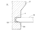
図1において、10はこの発明の一実施例に係る半導体ウェーハの外周部の保護膜エッチング装置(以下、保護膜エッチング装置)で、この保護膜エッチング装置10は、装置架台11と、溝幅がシリコンウェーハWの厚さと略等しい環状溝12aを外周面に有するエッチング回転治具12と、エッチング回転治具12の回転モータ(回転手段)13と、エッチング回転治具12とシリコンウェーハWとを相対的に移動し、常時、シリコンウェーハWの外周部の最外周縁と環状溝12aの奥壁12bとの間に空隙aを形成して(図2)、シリコンウェーハWの外周部を環状溝12aに配置するXYテーブル(移動手段、倣い手段)14と、環状溝12aにエッチング液を供給するディスペンサ(エッチング液供給手段)15とを備えている。シリコンウェーハWは、厚さ725μm、直径200mmで、シリコン酸化膜Waが形成されている。
In FIG. 1,
装置架台11は、正面視してコの字形を有する部材で、その上面に回転モータ13が固着されている。装置架台11の上部には、貫通孔11aが形成されている。貫通孔11aを通して、回転モータ13の出力シャフト13aが下方に向かって突出している。出力シャフト13aの先端部には、ジョイント16を介して、長尺な回転シャフト17が着脱自在に連結されている。回転シャフト17の下端部は大径化され、この大径部分にエッチング液を貯留する上戸形状の貯液部18が形成されている。この貯液部18の形状は密閉型のスリップリングとしても良い。また、回転シャフト17の大径部分には、その軸線に沿って、エッチング回転治具12が着脱自在に挿着される治具挿着孔17aが形成されている。治具挿着孔17aの上端は、貯液部18の下部位置まで達している。この回転シャフト17の貯液部18の下部には、治具挿着孔17aの上端部と連通する液導出孔17bが形成されている。貯液部18には、微細な吐出管19を介して、ディスペンサ15から吐出されたエッチング液が供給される。ディスペンサ15には、供給量0.0001cc/shotのピエゾポンプが採用されている。エッチング液は50重量%、HF溶液である。回転シャフト17の大径部分の側壁には、1つのねじ孔17cが形成されている。ねじ孔17cには、エッチング回転治具12を側方から締結する固定ねじ20が螺合されている。
The
エッチング回転治具12は、軸線を中心に回転する円柱形状の治具本体21を有している。治具本体21としては、直径3mm、空孔径5μm、空孔率35%の高密度ポリエチレンが採用されている。治具本体21の下端部の外周面には、前記環状溝12aが形成されている。治具本体21の環状溝12aの奥壁12b部分の直径は1.8mm、環状溝12aの溝幅は、シリコンウェーハWの厚さより若干狭い700μm、環状溝12aの深さは0.6mmである。この深さは、ウェーハ外周部のシリコン酸化膜Waのエッチング時に、常時、環状溝12aに配置されたウェーハ外周部の最外周縁と、環状溝12aの奥壁12bとの間に空隙aが形成される長さである(図2)。また、エッチング回転治具12の環状溝12aの奥壁12b部分の半径は、シリコンウェーハWの外周部に形成されたノッチ部nのウェーハ半径方向の長さ0.9mmより若干短い。
The
エッチング回転治具12の直径と環状溝12aの奥部分の直径との関係は、シリコン酸化膜Waがエッチングされる膜除去幅の狙い値に応じて適宜変更される。
XYテーブル14の上部には、シリコンウェーハWを真空吸着する小径なウェーハ保持板22を回転するウェーハ回転モータ23が固着されている。
The relationship between the diameter of the etching
A
次に、一実施例に係る保護膜エッチング装置10を用いた半導体ウェーハの外周部の保護膜エッチング方法を説明する。
Next, a method for etching a protective film on the outer periphery of a semiconductor wafer using the protective
回転モータ13によりエッチング回転治具12を60rpmで回転させながら、ディスペンサ15より0.001cc/shotでエッチング液を貯液部18に間欠供給する。貯液部18のエッチング液は、液導出孔17bを介してエッチング回転治具12の上端部に供給される。エッチング回転治具12は吸水性が高い高密度ポリエチレンである。よって、エッチング液はそのまま徐々に下降し、環状溝12aが形成された下端部まで伝わる。こうして、エッチング液は環状溝12aの形成壁から、環状溝12aの内部空間に徐々に染み出す。
While rotating the etching
また、シリコンウェーハWはウェーハ保持板22に真空吸着され、ウェーハ回転モータ23により10rpmで回転される。その後、回転中のシリコンウェーハWは、XYテーブル14によりエッチング回転治具12に近接され、そのウェーハ外周部がエッチング回転治具12の環状溝12aに挿入される。このとき、ウェーハ外周部の最外周縁と環状溝12aの奥壁12bとの間には、常時、空隙aが形成され、シリコンウェーハWとエッチング回転治具12とが非接触状態で保持される(図3)。この状態のまま、シリコンウェーハWの外周部のシリコン酸化膜Waをエッチングする。ウェーハ全周のエッチング時間は70秒、このうちノッチ部nのエッチングに要する時間は10秒である。
また、酸化膜エッチング中、エッチング回転治具12およびシリコンウェーハWを回転させながら、XYテーブル14によりシリコンウェーハWのエッチング回転治具12に対する距離を調整する。これにより、エッチング回転治具12をシリコンウェーハWの外周部形状に倣い動かして酸化膜エッチングすることができる。その結果、シリコンウェーハWの外周部の全域にわたってシリコン酸化膜Waのウェーハ半径方向のエッチング幅の均一化が可能になる。
Further, the silicon wafer W is vacuum-sucked on the
Further, the distance between the silicon wafer W and the
このように、ウェーハ外周部の最外周縁と環状溝12aの奥壁12bとを非接触状態にしたまま、ウェーハ外周部のシリコン酸化膜Waをエッチングするので、ノッチ部nを含むウェーハ外周部が損傷しない。また、環状溝12aの奥壁12bが摩耗しないため、溝深さが一定のままシリコン酸化膜Waのウェーハ半径方向のエッチング幅の均一化が図れる。
さらに、エッチング回転治具12の環状溝12aの奥壁12b部分の半径は、ノッチ部nのウェーハ半径方向の最大長さより短い。そのため、例えばエッチング回転治具12の環状溝12aの奥壁12b部分の半径を、ノッチ部nのウェーハ半径方向の最大長さより長くした場合に比べて(図4)、ノッチ部nの内部空間におけるエッチング回転治具12の自由度が大きくなる。これにより、エッチング回転治具12の外周部がノッチ部nに接触するおそれが低減する。よって、ノッチ部nの全域にわたって、ノッチ部nの外縁に直交するシリコン酸化膜Waのエッチング幅を略均一にすることができる。
Thus, the silicon outer peripheral portion of the wafer is etched while the outermost peripheral edge of the wafer outer peripheral portion and the
Further, the radius of the
10 半導体ウェーハの外周部の保護膜エッチング装置、
12 エッチング回転治具、
12a 環状溝、
12b 奥壁、
13 回転モータ(回転手段)、
14 XYテーブル(移動手段、倣い手段)、
15 ディスペンサ(エッチング液供給手段)、
21 治具本体、
W シリコンウェーハ(半導体ウェーハ)、
Wa シリコン酸化膜(保護膜)、
a 空隙。
10. A protective film etching apparatus for the outer periphery of a semiconductor wafer,
12 Etching rotating jig,
12a annular groove,
12b back wall,
13 Rotating motor (rotating means),
14 XY table (moving means, copying means),
15 dispenser (etching solution supply means),
21 Jig body,
W Silicon wafer (semiconductor wafer),
Wa Silicon oxide film (protective film),
a Void.
Claims (8)
略円柱体または略円筒体であるエッチング回転治具の外周面に形成された前記半導体ウェーハの厚さと溝幅が略等しい環状溝に、その環状溝の奥壁との間に常時空隙を有して上記半導体ウェーハの外周部を挿入し、
この環状溝にエッチング液を供給しながら、上記エッチング回転治具をその軸線回りに回転させる半導体ウェーハの外周部の保護膜エッチング方法。 A method of etching a protective film of a semiconductor wafer having a protective film on the outer periphery,
The annular groove formed on the outer peripheral surface of the etching rotary jig that is a substantially cylindrical body or a substantially cylindrical body has a gap between the thickness of the semiconductor wafer and the groove wall that is substantially equal to the inner wall of the annular groove. Insert the outer periphery of the semiconductor wafer,
A method of etching a protective film on an outer peripheral portion of a semiconductor wafer, wherein the etching rotary jig is rotated about its axis while supplying an etching solution to the annular groove.
このエッチング回転治具をその軸線回りに回転させる回転手段と、
半導体ウェーハの外周部の最外周縁と環状溝の奥壁との間に空隙を形成するように、この半導体ウェーハの外周部を環状溝内に挿入する手段と、
前記環状溝にエッチング液を供給するエッチング液供給手段とを備えた半導体ウェーハ外周部の保護膜エッチング装置。 An etching rotary jig comprising a substantially cylindrical body or a substantially cylindrical body having an annular groove on the outer peripheral surface thereof having a groove width substantially equal to the thickness of the semiconductor wafer;
Rotating means for rotating the etching rotating jig around its axis,
Means for inserting the outer peripheral portion of the semiconductor wafer into the annular groove so as to form a gap between the outermost peripheral edge of the outer peripheral portion of the semiconductor wafer and the inner wall of the annular groove;
A protective film etching apparatus for an outer peripheral portion of a semiconductor wafer, comprising an etching solution supply means for supplying an etching solution to the annular groove.
この治具本体の外周面に、その溝幅が半導体ウェーハの厚さと略等しくなるように形成され、エッチング液が供給されるとともに、保護膜を有する半導体ウェーハの外周部が挿入される環状溝とを備え、
半導体ウェーハの外周部がその最外周縁と前記環状溝の奥壁との間に空隙を形成するようこの環状溝に挿入され、環状溝に供給されたエッチング液により、半導体ウェーハの外周部の保護膜がエッチングされるエッチング用回転治具。 A jig body made of a substantially cylindrical body or a substantially cylindrical body that rotates about its axis;
An annular groove is formed on the outer peripheral surface of the jig body so that the groove width is substantially equal to the thickness of the semiconductor wafer, the etching liquid is supplied, and the outer peripheral portion of the semiconductor wafer having the protective film is inserted. With
The outer periphery of the semiconductor wafer is inserted into the annular groove so as to form a gap between the outermost peripheral edge and the inner wall of the annular groove, and the outer periphery of the semiconductor wafer is protected by the etching solution supplied to the annular groove. An etching rotating jig in which a film is etched.
Priority Applications (1)
| Application Number | Priority Date | Filing Date | Title |
|---|---|---|---|
| JP2004111471A JP4178520B2 (en) | 2004-04-05 | 2004-04-05 | Method and apparatus for etching protective film on outer periphery of semiconductor wafer, and rotating jig for etching |
Applications Claiming Priority (1)
| Application Number | Priority Date | Filing Date | Title |
|---|---|---|---|
| JP2004111471A JP4178520B2 (en) | 2004-04-05 | 2004-04-05 | Method and apparatus for etching protective film on outer periphery of semiconductor wafer, and rotating jig for etching |
Publications (2)
| Publication Number | Publication Date |
|---|---|
| JP2005294764A true JP2005294764A (en) | 2005-10-20 |
| JP4178520B2 JP4178520B2 (en) | 2008-11-12 |
Family
ID=35327317
Family Applications (1)
| Application Number | Title | Priority Date | Filing Date |
|---|---|---|---|
| JP2004111471A Expired - Lifetime JP4178520B2 (en) | 2004-04-05 | 2004-04-05 | Method and apparatus for etching protective film on outer periphery of semiconductor wafer, and rotating jig for etching |
Country Status (1)
| Country | Link |
|---|---|
| JP (1) | JP4178520B2 (en) |
Cited By (2)
| Publication number | Priority date | Publication date | Assignee | Title |
|---|---|---|---|---|
| JP2009117762A (en) * | 2007-11-09 | 2009-05-28 | Kazuo Tanabe | Wafer edge etching method and apparatus. |
| JP2010093082A (en) * | 2008-10-08 | 2010-04-22 | Tokyo Electron Ltd | Removing method and processing device of polysilicon film, and storage medium |
-
2004
- 2004-04-05 JP JP2004111471A patent/JP4178520B2/en not_active Expired - Lifetime
Cited By (2)
| Publication number | Priority date | Publication date | Assignee | Title |
|---|---|---|---|---|
| JP2009117762A (en) * | 2007-11-09 | 2009-05-28 | Kazuo Tanabe | Wafer edge etching method and apparatus. |
| JP2010093082A (en) * | 2008-10-08 | 2010-04-22 | Tokyo Electron Ltd | Removing method and processing device of polysilicon film, and storage medium |
Also Published As
| Publication number | Publication date |
|---|---|
| JP4178520B2 (en) | 2008-11-12 |
Similar Documents
| Publication | Publication Date | Title |
|---|---|---|
| CN101412201B (en) | Carrier, method for its application and method for simultaneous double-sided material removal processing of semiconductor wafers | |
| TWI353006B (en) | Method for manufacturing epitaxial wafer | |
| JP2004507085A (en) | Method and apparatus for processing a semiconductor wafer using a novel final polishing method | |
| TW200920661A (en) | Retaining ring with shaped profile | |
| US20120118320A1 (en) | Methods for Isolated Bevel Edge Clean | |
| US6918864B1 (en) | Roller that avoids substrate slippage | |
| KR20070096934A (en) | Polishing pads, polishing methods and polishing devices | |
| US20190099855A1 (en) | Polishing apparatus | |
| CN100530557C (en) | Etching method of single wafer | |
| TWI334622B (en) | Unpolished semiconductor wafer and method for producing an unpolished semiconductor wafer | |
| TW200414970A (en) | Polishing pad and its polishing method | |
| JP4178520B2 (en) | Method and apparatus for etching protective film on outer periphery of semiconductor wafer, and rotating jig for etching | |
| JP2010040549A (en) | Semiconductor wafer and manufacturing method thereof | |
| CN103419124A (en) | Retainer ring | |
| JP2007208060A (en) | Silicon wafer manufacturing method, silicon wafer and silicon block | |
| JP2016049579A (en) | Core drill and core drill equipment | |
| JP2011098396A (en) | Lapping surface plate and lapping method | |
| US6572461B2 (en) | Method for producing wafer notches with rounded corners and a tool therefor | |
| JP6253206B2 (en) | Blade processing apparatus and blade processing method | |
| US20150021498A1 (en) | Chemical mechanical polishing retaining ring methods and apparatus | |
| JP4816229B2 (en) | Wafer single wafer etching system | |
| JP5343099B2 (en) | Semiconductor wafer polishing method | |
| JP5343400B2 (en) | Manufacturing method of semiconductor wafer | |
| JP4150266B2 (en) | Shower plate for plasma processing and manufacturing method thereof | |
| JP2018047551A (en) | Work processing apparatus and work processing method |
Legal Events
| Date | Code | Title | Description |
|---|---|---|---|
| A621 | Written request for application examination |
Free format text: JAPANESE INTERMEDIATE CODE: A621 Effective date: 20060627 |
|
| A977 | Report on retrieval |
Free format text: JAPANESE INTERMEDIATE CODE: A971007 Effective date: 20080410 |
|
| A131 | Notification of reasons for refusal |
Free format text: JAPANESE INTERMEDIATE CODE: A131 Effective date: 20080415 |
|
| A521 | Request for written amendment filed |
Free format text: JAPANESE INTERMEDIATE CODE: A523 Effective date: 20080616 |
|
| TRDD | Decision of grant or rejection written | ||
| A01 | Written decision to grant a patent or to grant a registration (utility model) |
Free format text: JAPANESE INTERMEDIATE CODE: A01 Effective date: 20080801 |
|
| A01 | Written decision to grant a patent or to grant a registration (utility model) |
Free format text: JAPANESE INTERMEDIATE CODE: A01 |
|
| A61 | First payment of annual fees (during grant procedure) |
Free format text: JAPANESE INTERMEDIATE CODE: A61 Effective date: 20080814 |
|
| R150 | Certificate of patent or registration of utility model |
Ref document number: 4178520 Country of ref document: JP Free format text: JAPANESE INTERMEDIATE CODE: R150 Free format text: JAPANESE INTERMEDIATE CODE: R150 |
|
| FPAY | Renewal fee payment (event date is renewal date of database) |
Free format text: PAYMENT UNTIL: 20110905 Year of fee payment: 3 |
|
| FPAY | Renewal fee payment (event date is renewal date of database) |
Free format text: PAYMENT UNTIL: 20120905 Year of fee payment: 4 |
|
| R250 | Receipt of annual fees |
Free format text: JAPANESE INTERMEDIATE CODE: R250 |
|
| FPAY | Renewal fee payment (event date is renewal date of database) |
Free format text: PAYMENT UNTIL: 20130905 Year of fee payment: 5 |
|
| R250 | Receipt of annual fees |
Free format text: JAPANESE INTERMEDIATE CODE: R250 |
|
| R250 | Receipt of annual fees |
Free format text: JAPANESE INTERMEDIATE CODE: R250 |
|
| R250 | Receipt of annual fees |
Free format text: JAPANESE INTERMEDIATE CODE: R250 |
|
| R250 | Receipt of annual fees |
Free format text: JAPANESE INTERMEDIATE CODE: R250 |
|
| R250 | Receipt of annual fees |
Free format text: JAPANESE INTERMEDIATE CODE: R250 |
|
| R250 | Receipt of annual fees |
Free format text: JAPANESE INTERMEDIATE CODE: R250 |
|
| R250 | Receipt of annual fees |
Free format text: JAPANESE INTERMEDIATE CODE: R250 |
|
| R250 | Receipt of annual fees |
Free format text: JAPANESE INTERMEDIATE CODE: R250 |
|
| R250 | Receipt of annual fees |
Free format text: JAPANESE INTERMEDIATE CODE: R250 |
|
| R250 | Receipt of annual fees |
Free format text: JAPANESE INTERMEDIATE CODE: R250 |
|
| R250 | Receipt of annual fees |
Free format text: JAPANESE INTERMEDIATE CODE: R250 |
|
| R250 | Receipt of annual fees |
Free format text: JAPANESE INTERMEDIATE CODE: R250 |
|
| EXPY | Cancellation because of completion of term |