JP2005294732A - Method for creating conductive property region - Google Patents
Method for creating conductive property region Download PDFInfo
- Publication number
- JP2005294732A JP2005294732A JP2004111043A JP2004111043A JP2005294732A JP 2005294732 A JP2005294732 A JP 2005294732A JP 2004111043 A JP2004111043 A JP 2004111043A JP 2004111043 A JP2004111043 A JP 2004111043A JP 2005294732 A JP2005294732 A JP 2005294732A
- Authority
- JP
- Japan
- Prior art keywords
- region
- semiconductor substrate
- type
- conductive property
- concentration
- Prior art date
- Legal status (The legal status is an assumption and is not a legal conclusion. Google has not performed a legal analysis and makes no representation as to the accuracy of the status listed.)
- Pending
Links
Images
Landscapes
- Insulated Gate Type Field-Effect Transistor (AREA)
Abstract
【課題】 イオン注入法を利用して半導体基板内に導電特性領域を作成すると、イオン注入された不純物の拡散量が大きいために、微小な導電特性領域を局所的に作成することが困難であった。
【解決手段】 半導体基板内に周囲の導電特性から相違する導電特性を有する異導電特性領域を作成する方法である。半導体基板内の所定領域をレーザを利用して300〜600℃の温度に局所的に加熱する工程を備えている。この加熱処理する工程によって局所領域に酸素ドナーを発生させ、この酸素ドナーの発生量に基づいて半導体基板内に微小な導電特性領域を作成することを特徴としている。
【選択図】 なしPROBLEM TO BE SOLVED: To create a small conductive characteristic region locally when a conductive characteristic region is created in a semiconductor substrate by using an ion implantation method because of a large diffusion amount of the ion-implanted impurity. It was.
A method of creating a different conductive characteristic region having a conductive characteristic different from a surrounding conductive characteristic in a semiconductor substrate. There is a step of locally heating a predetermined region in the semiconductor substrate to a temperature of 300 to 600 ° C. using a laser. According to this heat treatment step, oxygen donors are generated in the local region, and a minute conductive property region is created in the semiconductor substrate based on the generated amount of oxygen donors.
[Selection figure] None
Description
本発明は、半導体基板内に周囲の導電特性から相違する微小な導電特性領域を作成する技術に関する。また、微小な導電特性領域を備える半導体装置に関する。本明細書でいう導電特性とは、n型、p型の導電型、さらにはその導電型領域の実質的な不純物量の違いを含めた特性のことをいう。同一の導電型であってもその実質的な不純物量が異なれば、その導電特性は相違しているという。なお、本明細書では、酸素ドナーも不純物の一つに含まれる。 The present invention relates to a technique for creating a minute conductive characteristic region in a semiconductor substrate that differs from the surrounding conductive characteristics. In addition, the present invention relates to a semiconductor device including a minute conductive characteristic region. The conductive characteristic referred to in this specification refers to a characteristic including n-type and p-type conductivity types, and a substantial impurity amount difference in the conductivity type region. Even if they are of the same conductivity type, their conductivity characteristics are different if their substantial impurity amounts are different. Note that in this specification, an oxygen donor is also included as one of impurities.
半導体装置が小型化されるとその機能の向上や消費電力の低減化などに有効なことから、半導体装置の小型化への要求は強い。半導体装置の小型化を実現するためには、その半導体装置内に形成されている導電特性領域を微小に作成する製造技術が必須である。また、現状の半導体装置のサイズであっても、半導体装置の耐圧やオン抵抗の改善を図るために、半導体装置内に微小な導電特性領域を局所的に作成する技術が要望されている。いずれも微小な導電特性領域を作成することが重要である。
あるいは、半導体基板にセンサ素子などが形成されたマイクロ構造体が知られている。この種の構造体の微小化を図る場合にも、微小な導電特性領域を局所的に作成する技術が重要である。
When a semiconductor device is miniaturized, it is effective for improving its function and reducing power consumption. Therefore, there is a strong demand for miniaturization of the semiconductor device. In order to realize miniaturization of a semiconductor device, a manufacturing technique for creating a minute conductive property region formed in the semiconductor device is essential. Further, there is a demand for a technique for locally creating a minute conductive characteristic region in a semiconductor device in order to improve the breakdown voltage and on-resistance of the semiconductor device even if the size of the semiconductor device is the current size. In any case, it is important to create a minute conductive property region.
Alternatively, a microstructure having a sensor element or the like formed on a semiconductor substrate is known. Even when this type of structure is miniaturized, a technique for locally creating a minute conductive property region is important.
微小な導電性特性領域が局所的に形成されている半導体装置の一例として、LDD(Lightly Doped Drain)構造を備える半導体装置が知られている。LDD構造とは、半導体基板の表面に沿って形成されるn型高濃度ドレイン領域とp型ボディ領域の間に介在するn型の低濃度の導電特性領域のことを言う。必要であれば、n型高濃度ソース領域とp型ボディ領域の間にもn型の低濃度の導電特性領域を介在させてもよく、この構造もLDD構造と称する場合がある。このn型高濃度ドレイン領域とp型ボディ領域の界面近傍には電界が集中し易い。LDD構造とは、その電界の集中し易い領域のみを局所的に濃度を薄くすることで電界集中を緩和して耐圧を向上させる技術である。このLDD構造は、電界の集中し易い箇所に一致して形成されると耐圧の向上に有効であるが、このLDD構造がその周辺にまで大きく形成されてしまうと、オン抵抗の増大などの原因となり問題である。 As an example of a semiconductor device in which a minute conductive characteristic region is locally formed, a semiconductor device having an LDD (Lightly Doped Drain) structure is known. The LDD structure refers to an n-type low-concentration conductive property region interposed between an n-type high-concentration drain region and a p-type body region formed along the surface of a semiconductor substrate. If necessary, an n-type low-concentration conductive characteristic region may be interposed between the n-type high-concentration source region and the p-type body region, and this structure may also be referred to as an LDD structure. The electric field tends to concentrate near the interface between the n-type heavily doped drain region and the p-type body region. The LDD structure is a technique for improving the breakdown voltage by relaxing the concentration of the electric field only in a region where the electric field is likely to concentrate, thereby locally reducing the concentration. This LDD structure is effective in improving the withstand voltage when formed in conformity with a location where electric field tends to concentrate. However, if this LDD structure is formed to a large extent around it, it causes an increase in on-resistance. It becomes a problem.
このLDD構造は半導体基板の所定領域に対して不純物をイオン注入した後に、高温のアニール工程を実施して注入した不純物を拡散させて形成される。不純物をイオン注入すると、その箇所に結晶欠陥が生じる。したがって、この結晶欠陥を回復させるために、通常は800℃以上のアニール工程を実施する必要があり、このアニール工程が不十分だとリーク電流などの原因となる。そのため、イオン注入を利用する製造方法では高温でのアニール工程が必須である。しかしながら、この高温のアニール工程を実施すると、注入された不純物は等方的に広く拡散するために微小な導電特性領域を形成するのが困難という問題がある。
特許文献1では、ランプアニールを利用し、短時間の高温処理を施すことで過度な拡散を抑制する技術を報告しているが、この技術を利用したとしても微小な導電特性領域を形成するのには限界がある。したがって、イオン注入法とは異なる方法により微小な導電特性領域を形成する製造技術の開発が望まれている。
Patent Document 1 reports a technique for suppressing excessive diffusion by using lamp annealing and performing high-temperature treatment for a short time, but even if this technique is used, a minute conductive characteristic region is formed. Has its limits. Therefore, development of a manufacturing technique for forming a minute conductive property region by a method different from the ion implantation method is desired.
上述したように、LDD構造のような微小な導電特性領域を半導体基板内に局所的に形成するためには、現状のイオン注入法ではその微小化に限界がある。また、微小な導電特性領域を局所的に形成するのみならず、半導体装置自体の小型化を実現するためにも、現状のイオン注入法ではその実現が困難と言える。また、各種のセンサ素子を備えたマイクロ構造体などの微小化を図るにも、微小な導電特性領域を作成する技術が望まれている。
本発明の一つの目的は、イオン注入法とは異なる手法を用いて、微小な導電特性領域を作成する製造方法の提供である。他の一つの目的は、その製造方法によって具現化される半導体装置を提供することである。
As described above, in order to locally form a minute conductive characteristic region such as an LDD structure in a semiconductor substrate, there is a limit to the miniaturization of the current ion implantation method. Moreover, it can be said that the current ion implantation method is difficult to realize not only the formation of a minute conductive characteristic region locally but also the miniaturization of the semiconductor device itself. In addition, a technique for creating a minute conductive property region is also desired in order to reduce the size of a microstructure including various sensor elements.
One object of the present invention is to provide a manufacturing method for creating a minute conductive property region by using a method different from the ion implantation method. Another object is to provide a semiconductor device embodied by the manufacturing method.
本発明は、半導体基板を低温(300〜600℃)で加熱処理したときに、その半導体基板内に発生する酸素ドナー(サーマルドナー)を利用して導電特性領域を作成する手法に立脚している。酸素ドナーとは、結晶格子間に存在している酸素原子が数個集まって一個の電子を放出する現象である。電子の数が増大するために、その半導体基板は実質的にn型化してくる。
従来から、チョコラルスキ(Czochralski;CZ)法で作成された半導体基板(単結晶シリコンウェハ)には、石英るつぼ中の溶解シリコンを引き上げる過程で、その石英るつぼから溶出した酸素が単結晶シリコンの格子間に侵入することが知られていた。しかしながら、この酸素が進入した状態で従来の半導体装置の製造プロセスを経由すると、半導体基板がさまざまな熱処理工程に曝されることから、発生する酸素ドナーによって半導体基板内の不純物濃度が変動する事態が頻発する。したがって、従来は製造プロセスを経由する前にドナーキリング(Donor Killing)工程を実施して、結晶格子間に侵入している酸素が除去された半導体基板を利用して半導体装置を製造していた。
本発明者らは、上記の現象に着眼するとともに、従来とは全く異なる発想から本発明を創作したのである。この酸素ドナーが発生する現象を積極的に利用することで導電特性領域を作成しようとするのである。即ち、結晶格子間に酸素が侵入した状態の半導体基板を敢えて利用して、その半導体基板に酸素ドナーを発生させて導電特性領域を作成するのである。
The present invention is based on a method of creating a conductive property region using an oxygen donor (thermal donor) generated in a semiconductor substrate when the semiconductor substrate is heat-treated at a low temperature (300 to 600 ° C.). . Oxygen donor is a phenomenon in which several oxygen atoms existing between crystal lattices gather to emit one electron. As the number of electrons increases, the semiconductor substrate becomes substantially n-type.
Conventionally, in a semiconductor substrate (single crystal silicon wafer) prepared by the Czochralski (CZ) method, oxygen eluted from the quartz crucible in the process of pulling up the dissolved silicon in the quartz crucible is interstitial between the lattices of the single crystal silicon. Was known to break into. However, when the conventional semiconductor device manufacturing process is performed in a state where oxygen has entered, the semiconductor substrate is exposed to various heat treatment processes, and thus the concentration of impurities in the semiconductor substrate may fluctuate due to the generated oxygen donor. Frequently occurs. Therefore, conventionally, a donor killing step is performed before going through the manufacturing process, and a semiconductor device is manufactured using a semiconductor substrate from which oxygen that has entered between crystal lattices has been removed.
The present inventors have focused on the above phenomenon and created the present invention from a completely different idea. The conductive characteristic region is created by actively utilizing the phenomenon that this oxygen donor is generated. In other words, a semiconductor substrate in which oxygen has entered between crystal lattices is intentionally used, and oxygen donors are generated in the semiconductor substrate to create a conductive characteristic region.
本発明は、半導体基板内に周囲の導電特性から相違する導電特性を有する異導電特性領域を作成する製造方法に具現化される。
本発明の一つの異導電特性領域を作成する製造方法は、半導体基板内の所定領域を300〜600℃の温度に局所的に加熱する工程を備えていることを特徴としている。
本発明で利用される半導体基板は、ドナーキリング工程を実施していない半導体基板や、あるいはドナーキリング工程を実施した後に半導体基板内に酸素を侵入させる処理を施したものを用いてもよい。
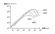
図1に、半導体基板を430〜480℃で加熱したときの処理時間と、発生する酸素ドナー量の関係を示す。酸素ドナーは、処理時間に対して一定の関係で増加していることが分かる。なお、加熱温度が300℃〜600℃の範囲内であれば、各処理温度における時間当たりの酸素ドナーの発生量は異なるが、処理時間に対して一定の関係で酸素ドナー量が増加することに変わりはない。
上記の製造方法によると、例えば、その不純物濃度が1×1012cm-3のp型の半導体基板に対して、加熱処理を実行して酸素ドナーを1×1012cm-3以上発生させたとすると、その半導体基板は実質的にn型の導電特性領域となる。つまり、発生する酸素ドナーがn型不純物と同様の作用をして、もともと存在していたp型不純物を相殺することになる。これによりp型の半導体基板がn型の導電特性領域に反転することになる。
なお、加熱温度と処理時間を調整して発生する酸素ドナー量を調整すれば、p+型の半導体基板をp−型の導電特性領域に変化させたり、あるいはn−型の半導体基板をn+型の導電特性領域に変化させたり、あるいは、もともと存在していたp型不純物と同等の酸素ドナーを発生させて実質的にi型の導電特性領域を形成することもできる。
この製造方法によると、加熱処理された領域で発生する酸素ドナーが、その周囲の領域へ拡散するという現象がほとんど起きないことから、加熱処理された領域のみを実質的にn型、またはp型、またはi型の微小な導電領域に変化させることができる。
The present invention is embodied in a manufacturing method for creating a different conductive property region having a conductive property different from a surrounding conductive property in a semiconductor substrate.
The manufacturing method for creating one different conductivity characteristic region of the present invention is characterized by including a step of locally heating a predetermined region in a semiconductor substrate to a temperature of 300 to 600 ° C.
The semiconductor substrate used in the present invention may be a semiconductor substrate that has not been subjected to the donor killing process, or a semiconductor substrate that has been subjected to a treatment for allowing oxygen to enter the semiconductor substrate after the donor killing process has been performed.
FIG. 1 shows the relationship between the treatment time when the semiconductor substrate is heated at 430 to 480 ° C. and the amount of oxygen donor generated. It can be seen that the oxygen donor increases in a fixed relationship with the treatment time. If the heating temperature is in the range of 300 ° C. to 600 ° C., the amount of oxygen donor generated per hour at each processing temperature is different, but the oxygen donor amount increases in a fixed relationship with the processing time. There is no change.
According to the above manufacturing method, for example, when a p-type semiconductor substrate having an impurity concentration of 1 × 10 12 cm −3 is subjected to heat treatment, oxygen donors are generated at 1 × 10 12 cm −3 or more. Then, the semiconductor substrate substantially becomes an n-type conductive property region. That is, the generated oxygen donor acts in the same manner as the n-type impurity, and cancels the p-type impurity that originally existed. As a result, the p-type semiconductor substrate is inverted to the n-type conductive characteristic region.
If the amount of oxygen donor generated by adjusting the heating temperature and the processing time is adjusted, the p + type semiconductor substrate is changed to a p − type conductive property region, or the n − type semiconductor substrate is changed to n +. The i-type conductive property region can be formed by changing to a conductive property region of a type or by generating an oxygen donor equivalent to the p-type impurity originally present.
According to this manufacturing method, the phenomenon that the oxygen donor generated in the heat-treated region diffuses to the surrounding region hardly occurs, so that only the heat-treated region is substantially n-type or p-type. Or an i-type minute conductive region.
本発明の他の一つの異導電特性領域を作成する製造方法は、半導体基板内の所定領域を含むより広範な領域を300〜600℃の温度に加熱する工程を有している。その工程が実施された後に、半導体基板内の所定領域を700℃以上の温度に局所的に加熱する工程を有している。
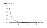
図2に、半導体基板を700℃で加熱処理したときの処理時間と、半導体基板内の酸素ドナー量の関係を示している。この結果では、処理時間が0のときにすでに半導体基板内には約1×1016cm-3の酸素ドナーが存在している。つまり、この結果は半導体基板を300〜600℃の温度で一旦加熱処理して約1×1016cm-3の酸素ドナーを発生させた後に、700℃の高温で加熱処理したときの結果である。酸素ドナーは700℃という高温になると処理時間と一定の関係で減少することが分かる。
この現象から、例えば、p型の半導体基板の全体を300〜600℃の温度に加熱する工程によりn型に一旦変化させた後に、所定領域のみを700℃以上の温度で局所的に加熱する工程を実行してその局所領域の酸素ドナーを消失させ、p型の導電特性領域に再度戻すという製造方法が可能であることが分かる。したがって、p型の導電特性領域を微小に作成可能であることが分かる。
同様に、p型の半導体基板の全体をp−型に一旦変化させた後に、所定領域のみを高温で加熱処理することで微小なp+型の導電特性領域を作成してもよいし、n型の半導体基板の全体をn+型に一旦変化させた後に、所定領域のみを高温で加熱処理することで微小なn−型の導電特性領域を作成してもよく、あるいはi型の微小な導電特性領域を作成してもよい。
Another manufacturing method for producing a different conductivity characteristic region of the present invention includes a step of heating a wider region including a predetermined region in a semiconductor substrate to a temperature of 300 to 600 ° C. After the step is carried out, there is a step of locally heating a predetermined region in the semiconductor substrate to a temperature of 700 ° C. or higher.
FIG. 2 shows the relationship between the treatment time when the semiconductor substrate is heated at 700 ° C. and the amount of oxygen donor in the semiconductor substrate. In this result, when the processing time is 0, an oxygen donor of about 1 × 10 16 cm −3 already exists in the semiconductor substrate. In other words, this result is a result when the semiconductor substrate is heat-treated at a temperature of 300 to 600 ° C. to generate an oxygen donor of about 1 × 10 16 cm −3 and then heat-treated at a high temperature of 700 ° C. . It can be seen that the oxygen donor decreases at a high temperature of 700 ° C. with a certain relationship with the processing time.
From this phenomenon, for example, after the entire p-type semiconductor substrate is changed to n-type by a process of heating the entire p-type semiconductor substrate to a temperature of 300 to 600 ° C., only a predetermined region is locally heated at a temperature of 700 ° C. or higher. It can be seen that a manufacturing method is possible in which the oxygen donor in the local region is eliminated and returned to the p-type conductive property region again. Therefore, it can be seen that a p-type conductive characteristic region can be made minutely.
Similarly, after the entire p-type semiconductor substrate is changed to the p − type once, only a predetermined region may be heat-treated at a high temperature to create a minute p + type conductive characteristic region, or n After the entire semiconductor substrate of the type is changed to the n + type, a minute n − type conductive characteristic region may be created by heat-treating only a predetermined region at a high temperature, or an i type minute substrate A conductive property region may be created.
局所的加熱工程では、電子ビーム又はレーザを半導体基板の所定領域に局所的に照射することが好ましい。
電子ビームやレーザ装置を利用すると、半導体基板内の所定領域のみを局所的に加熱することが容易である。製造方法が簡単化される。
In the local heating step, it is preferable to locally irradiate a predetermined region of the semiconductor substrate with an electron beam or a laser.
When an electron beam or a laser device is used, it is easy to locally heat only a predetermined region in the semiconductor substrate. The manufacturing method is simplified.
本発明をMOSFET、IGBT、サイリスタなどの半導体装置の製造方法に適用すると好適である。
本発明の一つの半導体装置の製造方法は、半導体基板の表面に沿って、n型高濃度領域と、p型ボディ領域と、両領域間に介在するn型低濃度導電特性領域を備える半導体装置の製造方法に具現化される。本発明の製造方法の特徴は、この半導体装置のp型半導体基板のn型低濃度導電特性領域を作成する領域を300〜600℃の温度に局所的に加熱する工程を備えていることである。
この製造方法を実施すると、n型高濃度領域とp型ボディ領域の両領域間であって電界の集中し易い箇所のみに、n型低濃度導電特性領域を容易に作成することができる。オン抵抗などの他の特性を劣化させることなく、耐圧を向上させることができる。
The present invention is preferably applied to a method for manufacturing a semiconductor device such as a MOSFET, IGBT, or thyristor.
According to one aspect of the present invention, there is provided a semiconductor device manufacturing method including an n-type high-concentration region, a p-type body region, and an n-type low-concentration conductive property region interposed between both regions along the surface of a semiconductor substrate. It is embodied in the manufacturing method. A feature of the manufacturing method of the present invention is that it includes a step of locally heating a region for forming an n-type low concentration conductive property region of a p-type semiconductor substrate of this semiconductor device to a temperature of 300 to 600 ° C. .
When this manufacturing method is carried out, an n-type low-concentration conductive characteristic region can be easily created only in a portion between both the n-type high-concentration region and the p-type body region and where the electric field tends to concentrate. The breakdown voltage can be improved without degrading other characteristics such as on-resistance.
本発明の他の一つの半導体装置の製造方法は、半導体基板の表面に沿って、p型高濃度領域と、n型ボディ領域と、両領域間に介在するp型低濃度導電特性領域を備える半導体装置の製造方法に具現化される。本発明の製造方法の特徴は、この半導体装置のp型半導体基板のp型低濃度導電特性領域を作成する領域を含むより広範な領域を300〜600℃の温度に加熱する工程を備えている。その後にp型手濃度特性領域を作成する領域を700℃以上の温度に局所的に加熱する工程を備えていることである。
この製造方法を実施すると、p型高濃度領域とn型ボディ領域の両領域間であって電界の集中し易い箇所のみに、p型低濃度導電特性領域を容易に作成することができる。オン抵抗などの他の特性を劣化させることなく、耐圧を向上させることができる。
Another method of manufacturing a semiconductor device according to the present invention includes a p-type high concentration region, an n-type body region, and a p-type low concentration conductive property region interposed between both regions along the surface of the semiconductor substrate. The present invention is embodied in a method for manufacturing a semiconductor device. A feature of the manufacturing method of the present invention includes a step of heating a wider region including a region for forming a p-type low-concentration conductive property region of a p-type semiconductor substrate of this semiconductor device to a temperature of 300 to 600 ° C. . Thereafter, a step of locally heating the region for creating the p-type hand density characteristic region to a temperature of 700 ° C. or higher is provided.
When this manufacturing method is carried out, the p-type low-concentration conductive characteristic region can be easily created only in the portion between the p-type high-concentration region and the n-type body region where the electric field tends to concentrate. The breakdown voltage can be improved without degrading other characteristics such as on-resistance.
本発明の技術思想が利用された半導体装置には、半導体装置自体にその特徴が現れている。即ち、半導体基板内に酸素ドナー濃度が1×1012cm-3以上である局所領域が形成されていることを特徴としている。
従来の半導体装置は、ドナーキリング工程を実施しているために、その半導体基板内の結晶格子間に酸素原子がほとんど存在していない。したがって、さまざまな熱処理工程を経た後であっても、その半導体基板内の酸素ドナー濃度が少なくとも1×1012cm-3以上存在していない。
一方、本発明の製造方法を利用した半導体基板内には、必然的に酸素ドナー濃度が大きい局所領域が形成されており、この特徴は本発明を利用していない技術と明確に区別され得る。したがって、半導体基板内に少なくとも1×1012cm-3以上の酸素ドナーが存在していれば、本発明の技術思想が利用された半導体装置と言える。
Features of the semiconductor device utilizing the technical idea of the present invention appear in the semiconductor device itself. That is, a local region having an oxygen donor concentration of 1 × 10 12 cm −3 or more is formed in the semiconductor substrate.
In the conventional semiconductor device, since the donor killing process is performed, oxygen atoms are hardly present between crystal lattices in the semiconductor substrate. Therefore, even after various heat treatment steps, the oxygen donor concentration in the semiconductor substrate does not exist at least 1 × 10 12 cm −3 or more.
On the other hand, a local region having a high oxygen donor concentration is inevitably formed in a semiconductor substrate using the manufacturing method of the present invention, and this feature can be clearly distinguished from a technique not using the present invention. Therefore, if an oxygen donor of at least 1 × 10 12 cm −3 or more exists in the semiconductor substrate, it can be said that the semiconductor device uses the technical idea of the present invention.
また、本発明の半導体装置を次のように特徴づけることもできる。
即ち、第1導電型の導電特性領域内に第2導電型の局所領域が形成されており、その第2導電型の局所領域の厚みが50nm以下であることを特徴としている。
従来のイオン注入法を利用して局所領域を形成すると、アニール工程による不純物の拡散によって、その局所領域の厚みは少なくとも50nm以上で形成されてしまう。この50nm以下の厚みの局所領域は、本発明の製造技術によって始めて具現化される範囲であり、従来の半導体装置とは明確に区別することができる。
The semiconductor device of the present invention can also be characterized as follows.
That is, a local region of the second conductivity type is formed in the conductive characteristic region of the first conductivity type, and the thickness of the local region of the second conductivity type is 50 nm or less.
When a local region is formed using a conventional ion implantation method, the local region is formed with a thickness of at least 50 nm or more due to diffusion of impurities in the annealing process. This local region having a thickness of 50 nm or less is a range that is first realized by the manufacturing technique of the present invention, and can be clearly distinguished from conventional semiconductor devices.
本発明によると、半導体基板内に実質的にn型、またはp型、またはi型の微小な導電特性領域を作成する製造方法を提供することができる。また、その製造方法を利用して微小な導電特性領域を備える半導体装置を提供することができる。 According to the present invention, it is possible to provide a manufacturing method in which a minute conductive characteristic region of substantially n-type, p-type, or i-type is formed in a semiconductor substrate. In addition, a semiconductor device including a minute conductive characteristic region can be provided using the manufacturing method.
最初に実施例の主要な特徴を列記する。
(第1実施形態) 加熱の工程は、加熱する温度とその処理時間に基づいて制御される。酸素ドナーの発生量は加熱の温度と処理時間によって制御可能である。また、その酸素ドナーを消失させる場合も、その加熱の温度と処理時間によって消失量を制御可能である。したがって、両者を制御することで、所望する導電特性領域を作成することができる。
(第2実施形態) 半導体基板の所定領域を加温する手段として、レーザ装置や電子ビーム装置を用いて、その所定領域のみを加温することができる。あるいは、所定領域に開口部を有し、それ以外をマスク材で覆ってもよい。レーザ装置や電子ビーム装置を正確に走査しなくても所定領域のみを加温することができる。あるいは、断熱性を有するマスク材を用いて、その開口部から露出する半導体基板のみに熱が加わるようにしてもよい。
(第3実施形態) 隣接する導電特性領域の酸素ドナー濃度の差が1×1012cm-3以上である。酸素ドナーを利用する製造方法では、酸素ドナーを発生された導電特性領域とその周囲の導電特性領域、あるいは酸素ドナーを消失された導電特性領域とその周囲の導電特性領域には、酸素ドナーの濃度に必然的に差が生じる。この差は少なくとも1×1012cm-3以上である。この濃度差が生じている場合は、酸素ドナーを利用する製造方法が実施されたと言える。
(第4実施形態) 位置決め手段の一例として、レーザ装置と一体となって走査可能な位置調整装置が挙げられる。あるいは、ガルバノミラーなどの光学系を用いてレーザ光を所定の位置に照射可能にしてもよい。この場合、レーザ光の照射位置の位置決めが素早く実行可能となる。あるいは、半導体基板を移動可能な台に載置して、レーザ光が照射される位置に半導体基板自体を移動させて位置決めしてもよい。移動可能な台として、例えばピエゾステージなどで微小な移動を可能にし、微小は加工を実現してもよい。あるいは、次の製造工程までその載置されている半導体基板を移動可能な台と兼用させることで、製造ラインを簡単化させてもよい。その他に、レーザ光を照射したい箇所のみが開口しているマスクを半導体基板上に形成し、レーザ光を面的に照射させてもよい。この場合、微小な照射領域を実現するレーザ装置でなく、安価なレーザ装置を利用することができる。
First, the main features of the embodiment are listed.
First Embodiment The heating process is controlled based on the heating temperature and the processing time. The amount of oxygen donors generated can be controlled by the heating temperature and processing time. Also, when the oxygen donor is eliminated, the disappearance amount can be controlled by the heating temperature and the treatment time. Therefore, a desired conductive property region can be created by controlling both.
Second Embodiment As a means for heating a predetermined region of a semiconductor substrate, only the predetermined region can be heated using a laser device or an electron beam device. Or you may have an opening part in a predetermined area | region, and may cover the other with a mask material. Only a predetermined region can be heated without accurately scanning the laser device or the electron beam device. Alternatively, heat may be applied only to the semiconductor substrate exposed from the opening using a mask material having heat insulation properties.
Third Embodiment The difference in oxygen donor concentration between adjacent conductive property regions is 1 × 10 12 cm −3 or more. In the manufacturing method using the oxygen donor, the oxygen donor concentration is not included in the conductive property region in which the oxygen donor is generated and the surrounding conductive property region, or in the conductive property region in which the oxygen donor is eliminated and the surrounding conductive property region. There will necessarily be a difference. This difference is at least 1 × 10 12 cm −3 or more. When this difference in concentration occurs, it can be said that a manufacturing method using an oxygen donor has been carried out.
(Fourth Embodiment) As an example of the positioning means, there is a position adjusting device capable of scanning integrally with a laser device. Alternatively, a predetermined position may be irradiated with laser light using an optical system such as a galvanometer mirror. In this case, positioning of the irradiation position of the laser beam can be performed quickly. Alternatively, the semiconductor substrate may be placed on a movable table, and the semiconductor substrate itself may be moved to a position where the laser beam is irradiated. As a movable table, for example, a piezo stage or the like can be used to allow minute movement, and the minute can be processed. Alternatively, the manufacturing line may be simplified by using the semiconductor substrate placed thereon until the next manufacturing process also as a movable table. In addition, a mask in which only a portion where laser light is desired to be irradiated is formed on the semiconductor substrate, and the laser light may be irradiated on the surface. In this case, an inexpensive laser device can be used instead of a laser device that realizes a minute irradiation region.
図面を参照して以下に各実施例を詳細に説明する。なお、以下の実施例では、半導体装置内の微小な導電特性領域の一例として、横型MOSFETのLDD構造を参照して説明する。しかし、半導体装置内の微小な導電特性領域は本実施例のLDD構造に限るのもではなく、さまざまな構造に対して利用され得る。また、半導体装置自体が小型化されてくれば、いわゆるボディ領域自体やドリフト領域自体などが微小な導電特性領域となり、そのような領域に対して以下の実施例の技術思想を利用することができる。 Embodiments will be described in detail below with reference to the drawings. In the following embodiments, description will be made with reference to an LDD structure of a lateral MOSFET as an example of a minute conductive property region in a semiconductor device. However, the minute conductive characteristic region in the semiconductor device is not limited to the LDD structure of this embodiment, and can be used for various structures. If the semiconductor device itself is miniaturized, the so-called body region itself, drift region itself, and the like become minute conductive property regions, and the technical ideas of the following embodiments can be used for such regions. .
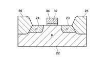
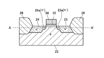
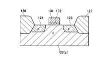
(第1実施例) 図3〜図5を用いて、第1実施例の横型のn型MOSFETのLDD構造の製造方法を説明する。まず、図3に、n型MOSFETの模式的な断面図を示す。
図示22は単結晶シリコンからなるp型の半導体基板22である。この半導体基板22の上部左右に酸化シリコンからなるフィールド酸化膜26が形成されている。図面右側のフィールド酸化膜26の端部に接するとともに、半導体基板22の表面にn+型のドレイン領域23が形成されている。
このドレイン領域23に対して半導体基板22によって隔てられた位置にn+型のソース領域24が形成されている。このソース領域24は、図面左側のフィールド酸化膜26の端部に接するとともに、半導体基板22の表面に形成されている。
ドレイン領域23とソース領域24は、図面左右に半導体基板22の表面に沿って形成されているとともに隔てられた位置関係に配置されている。この両者を隔てている半導体基板22はボディ領域などと称され、この領域に酸化シリコンからなるゲート絶縁膜32を介してゲート電極34が対向している。ゲート電極34はポリシリコンで形成されている。ゲート絶縁膜32とドレイン領域23及びソース領域24は直接接しておらず、所定の距離を隔てて離間している。
この半導体基板22やドレイン領域23やソース領域24の結晶格子間には酸素が存在している。いわゆるドナーキリング工程が実施されていない。
First Embodiment A method for manufacturing an LDD structure of a lateral n-type MOSFET according to a first embodiment will be described with reference to FIGS. First, FIG. 3 shows a schematic cross-sectional view of an n-type MOSFET.
22 shows a p-
An n + -
The
Oxygen exists between crystal lattices of the
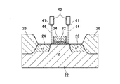
図4の図示41はレーザ装置であり、このレーザ装置41は位置調整装置42によって走査可能に支持されている。位置調整装置42は図示しないコンピュータによって制御される。なお、レーザ装置41と位置調整装置42が図面では左右に2個表示されているが、実際には位置調整装置42が走査して両者を兼用する。
レーザ装置41からは、波長が300〜800nmのレーザ光44が発振しており、このレーザ光44は、ゲート絶縁膜32とドレイン領域23及びソース領域24の間の半導体基板22の表面に照射される。レーザ光44が照射される半導体基板22は、このレーザ光44を吸収し、その光エネルギーが熱エネルギーに転換することにより加温される。加温される温度は、レーザ光44の波長やレーザ装置41の出力で制御可能であり、本実施例では450℃で所定時間照射される。
なお、位置調整装置42に代えて、例えばガルバノミラーなどの光学系を用いてレーザ光を所定の位置に照射可能にしてもよい。あるいは、半導体基板を移動可能な台に載置することで、レーザ光が照射される位置に半導体基板自体を移動されて位置決めしてもよい。あるいは、レーザ光を照射したい箇所のみが開口しているマスクを半導体基板上に形成し、レーザ光を面的に照射してもよい。
4 is a laser device, and this
A
In place of the
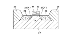
図5に示すように、レーザ光44が所定時間照射された箇所は、その結晶格子間に存在していた酸素原子が結合して酸素ドナー(サーマルドナー)を発生する。この酸素ドナーは、もともとその領域に存在していたp型の不純物を実質的に相殺するように作用する。いわゆるカウンタードーピングが実質的に生じることになる。したがって、p型の半導体基板22であった領域の一部がn−型に変化される。これによりドレイン側LDD領域23aがドレイン領域23と半導体基板22に介在する位置関係に形成され、ソース側LDD領域25aがソース領域24と半導体基板22に介在する位置関係に形成される。
この後に、アルミニウムなどをドレイン領域23上やソース領域24上にスパッタリングしてドレイン電極やソース電極を形成し、横型MOSFETが完成される。
As shown in FIG. 5, oxygen atoms existing between the crystal lattices are bonded to a portion irradiated with the
Thereafter, aluminum or the like is sputtered onto the
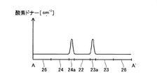
図6に、図5のA−A´に対応する酸素ドナー濃度を示す。横軸がA−A´線に対応しており、横軸の番号は各導電特性領域の番号に対応している。縦軸が酸素ドナー濃度である。この酸素ドナー濃度は、PL(Photoluminessennce)法やFT(Fourier Transform Infrared Spectroscopy)法やDLTS(Deep Level Transient Spectroscopy)法やドナーキリング前後のSR(Spreading Resistance)測定などの測定方法を用いて、酸素原子と区別して測定することができる。
レーザ光44が照射されたドレイン側LDD領域23aとソース側LDD領域24aで酸素濃度がピークを示している。その他の導電特性領域の酸素ドナーは一様に少なく、レーザ光44が照射された箇所と明確に区別できることが分かる。このドレイン側LDD領域23aとソース側LDD領域24aの酸素ドナー濃度は概ね1×1012cm-3以上である。あるいは、このドレイン側LDD領域23aとソース側LDD領域24aの酸素ドナー濃度は、その周囲の導電特性の酸素ドナー濃度よりも1×1012cm-3以上大きく形成されている。
この酸素ドナーが半導体基板22のp型不純物を実質的に相殺するために、ドレイン側LDD領域23aとソース側LDD領域24aはn-型に反転される。このとき、例えばイオン注入法のように結晶欠陥が生じることもないことから、リーク電流が発生するなどの問題が生じない。さらに、発生する酸素ドナーは、その周辺の領域に拡散する量が極めて少なく、したがってレーザ光44が照射された領域のみをドレイン側LDD領域23aとソース側LDD領域24aに変化することができる。具体的には半導体基板22の表面から50nm以下の微小な領域でも製造可能であり、これほどの微小化は従来のイオン注入法では実現不可能である。
また、このレーザ装置によるLDD構造の形成は、その製造プロセスが簡単化されるという利点もある。従来のイオン注入法では、マスクの形成、イオン注入、マスクの除去、そして高温アニールという工程を少なくとも実施する必要があるが、本実施例では実質的にレーザ光の照射のみであり、極めて簡単化されている。したがって、コストの低減化やTAT(Turn Around Time)の短縮化にも好適である。
FIG. 6 shows the oxygen donor concentration corresponding to AA ′ in FIG. The horizontal axis corresponds to the AA ′ line, and the number on the horizontal axis corresponds to the number of each conductive characteristic region. The vertical axis represents the oxygen donor concentration. This oxygen donor concentration is measured using a measurement method such as PL (Photoluminessennce) method, FT (Fourier Transform Infrared Spectroscopy) method, DLTS (Deep Level Transient Spectroscopy) method or SR (Spreading Resistance) measurement before and after donor killing. And can be measured separately.
The oxygen concentration peaks in the drain
Since the oxygen donor substantially cancels the p-type impurity of the
Further, the formation of the LDD structure by this laser device has an advantage that the manufacturing process is simplified. In the conventional ion implantation method, it is necessary to carry out at least the steps of mask formation, ion implantation, mask removal, and high-temperature annealing, but in this embodiment, only laser light irradiation is practically performed, which makes the process extremely simple. Has been. Therefore, it is suitable for cost reduction and TAT (Turn Around Time).
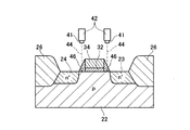
図7と図8に第1実施例の変形例を示す。
図7に示すように、この変形例はレーザ光44の照射位置に対応する半導体基板22上にスペーサー46が形成されている。このスペーサー46は酸化シリコンからなり、照射されるレーザ光44の一部を吸収し、半導体基板22に届くレーザ光44の光量を調整することができる。この変形例のスペーサー46は、ドレイン領域23及びソース領域24側に向けて傾斜して形成されている。
図8に示すように、スペーサー46を介してレーザ光44を半導体基板22に照射すると、ドレイン領域23とソース領域24の端部側では半導体基板22の深い位置までドレイン側LDD領域27とソース側LDD領域28が形成されるが、ゲート絶縁膜32側では半導体基板22の浅い位置までしか形成されない。これにより、ドレイン側LDD領域27とソース側LDD領域28が所定の屈曲率で形成される。本変形例では、その屈曲率が小さく形成されており、このドレイン側LDD領域27とソース側LDD領域28が緩やかにカーブしている。
この屈曲率は電界の集中に大きな影響を及ぼすことが知られており、本変形例のようにその屈曲率が小さいと、電界の集中をより緩和することが可能となる。ひいては耐圧が向上した半導体装置を実現できる。
なお、スペーサー46に代えて、レーザ装置41にフィルターを付けて、レーザ光をその照射する面内で光量分布が形成されるようにしてもよい。同様の作用効果を得ることができる。
7 and 8 show a modification of the first embodiment.
As shown in FIG. 7, in this modification, a
As shown in FIG. 8, when the
It is known that the bending rate has a great influence on the concentration of the electric field. If the bending rate is small as in this modification, the concentration of the electric field can be further relaxed. As a result, a semiconductor device with improved breakdown voltage can be realized.
Instead of the
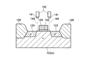
(第2実施例) 図9〜図11を用いて、第2実施例の横型のp型MOSFETのLDD構造の製造方法を説明する。図9に、p型MOSFETの模式的な断面図を示す。なお、第1実施例と略同一の構成要素に関してはその説明を省略する。第2実施例では、第1実施例と異なり、半導体基板122がp型で形成されている。
まず、このp型MOSFET全体を300℃〜600℃、好ましくは400℃〜500℃の温度で所定時間熱処理を実行する。すると、図10に示すように、半導体基板122がn型に変化する。このとき、ドレイン領域123とソース領域124も熱処理されるが、もともとp型の不純物を多く含んでいるために、n型に変化することはない。
次に、図10に示すように、レーザ装置141から波長が300〜800nmのレーザ光144が発振され、そのレーザ光144は、ゲート絶縁膜132とドレイン領域123及びソース領域124の間の半導体基板122に照射される。レーザ光144が照射される半導体基板122は、そのレーザ光144を吸収し、その光エネルギーが熱エネルギーに転換することにより加温される。加温される温度は、レーザ光144の波長やレーザ装置141の出力で制御可能であり、本実施例では700℃以上で所定時間加温される。
Second Embodiment A method for manufacturing an LDD structure of a lateral p-type MOSFET according to a second embodiment will be described with reference to FIGS. FIG. 9 shows a schematic cross-sectional view of a p-type MOSFET. Note that description of components that are substantially the same as those in the first embodiment is omitted. In the second embodiment, unlike the first embodiment, the
First, the entire p-type MOSFET is heat-treated at a temperature of 300 ° C. to 600 ° C., preferably 400 ° C. to 500 ° C. for a predetermined time. Then, as shown in FIG. 10, the
Next, as shown in FIG. 10,
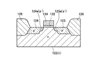
図11に示すように、レーザ光144が所定時間照射されたn型の半導体基板122は、p−型のドレイン側LDD領域123aとソース側LDD領域125aに変化される。これは、p型MOSFET全体を加温したときに半導体基板122に発生していた酸素ドナーが、700℃以上の加温によって消失することにより、もとより含まれていたp型の不純物が有利となってp型に再度変化したのである。このように、p型の微小な導電特性を形成する方法も例示された。
なお、第1実施例と同様に、スペーサーを介してレーザ光141を照射することで、屈曲率の小さいドレイン側LDD領域123aとソース側LDD領域125aを形成してもよい。さらに耐圧が向上されるp型MOSFETを製造することができる。
As shown in FIG. 11, the n-
As in the first embodiment, the drain-
以上、本発明の具体例を詳細に説明したが、これらは例示に過ぎず、特許請求の範囲を限定するものではない。特許請求の範囲に記載の技術には、以上に例示した具体例を様々に変形、変更したものが含まれる。
また、本明細書または図面に説明した技術要素は、単独であるいは各種の組合せによって技術的有用性を発揮するものであり、出願時請求項記載の組合せに限定されるものではない。また、本明細書または図面に例示した技術は複数目的を同時に達成し得るものであり、そのうちの一つの目的を達成すること自体で技術的有用性を持つものである。
Specific examples of the present invention have been described in detail above, but these are merely examples and do not limit the scope of the claims. The technology described in the claims includes various modifications and changes of the specific examples illustrated above.
The technical elements described in this specification or the drawings exhibit technical usefulness alone or in various combinations, and are not limited to the combinations described in the claims at the time of filing. In addition, the technology exemplified in this specification or the drawings can achieve a plurality of objects at the same time, and has technical usefulness by achieving one of the objects.
22:半導体基板
23:ドレイン領域
23a:ドレイン側LDD領域
24:ソース領域
24a:ソース側LDD領域
26:フィールド酸化膜
32:ゲート絶縁膜
34:ゲート電極
41:レーザ装置
42:位置調整装置
44:レーザ光
22: Semiconductor substrate 23:
Claims (7)
半導体基板の所定領域を300〜600℃の温度に局所的に加熱する工程を備えていることを特徴とする異導電特性領域の作成方法。 A method for creating a different conductive property region having a conductive property different from the surrounding conductive property in a semiconductor substrate,
A method for creating a different conductive property region, comprising a step of locally heating a predetermined region of a semiconductor substrate to a temperature of 300 to 600 ° C.
半導体基板の所定領域を含むより広範な領域を300〜600℃の温度に加熱する工程と、
その後に半導体基板の所定領域を700℃以上の温度に局所的に加熱する工程を備えていることを特徴とする異導電特性領域の作成方法。 A method for creating a different conductive property region having a conductive property different from the surrounding conductive property in a semiconductor substrate,
Heating a wider area including a predetermined area of the semiconductor substrate to a temperature of 300 to 600 ° C .;
And a step of locally heating a predetermined region of the semiconductor substrate to a temperature of 700 ° C. or higher.
p型半導体基板のn型低濃度導電特性領域を作成する領域を300〜600℃の温度に局所的に加熱する工程を備えていることを特徴とする半導体装置の製造方法。 A method of manufacturing a semiconductor device comprising an n-type high concentration region, a p-type body region, and an n-type low concentration conductive property region interposed between both regions along the surface of the semiconductor substrate,
A method for manufacturing a semiconductor device, comprising the step of locally heating a region for forming an n-type low-concentration conductive property region of a p-type semiconductor substrate to a temperature of 300 to 600 ° C.
p型半導体基板のp型低濃度導電特性領域を作成する領域を含むより広範な領域を300〜600℃の温度に加熱する工程と、
その後にp型低濃度導電特性領域を作成する領域を700℃以上の温度に局所的に加熱する工程を備えていることを特徴とする半導体装置の製造方法。 A method of manufacturing a semiconductor device comprising a p-type high concentration region, an n-type body region, and a p-type low concentration conductive property region interposed between both regions along the surface of the semiconductor substrate,
heating a broader region including a region for forming a p-type low-concentration conductive property region of a p-type semiconductor substrate to a temperature of 300 to 600 ° C .;
A method for manufacturing a semiconductor device comprising a step of locally heating a region for forming a p-type low-concentration conductive property region to a temperature of 700 ° C. or higher.
Priority Applications (1)
| Application Number | Priority Date | Filing Date | Title |
|---|---|---|---|
| JP2004111043A JP2005294732A (en) | 2004-04-05 | 2004-04-05 | Method for creating conductive property region |
Applications Claiming Priority (1)
| Application Number | Priority Date | Filing Date | Title |
|---|---|---|---|
| JP2004111043A JP2005294732A (en) | 2004-04-05 | 2004-04-05 | Method for creating conductive property region |
Publications (1)
| Publication Number | Publication Date |
|---|---|
| JP2005294732A true JP2005294732A (en) | 2005-10-20 |
Family
ID=35327290
Family Applications (1)
| Application Number | Title | Priority Date | Filing Date |
|---|---|---|---|
| JP2004111043A Pending JP2005294732A (en) | 2004-04-05 | 2004-04-05 | Method for creating conductive property region |
Country Status (1)
| Country | Link |
|---|---|
| JP (1) | JP2005294732A (en) |
Cited By (1)
| Publication number | Priority date | Publication date | Assignee | Title |
|---|---|---|---|---|
| JP2014160860A (en) * | 2014-05-01 | 2014-09-04 | Dainippon Screen Mfg Co Ltd | Heat treatment apparatus |
-
2004
- 2004-04-05 JP JP2004111043A patent/JP2005294732A/en active Pending
Cited By (1)
| Publication number | Priority date | Publication date | Assignee | Title |
|---|---|---|---|---|
| JP2014160860A (en) * | 2014-05-01 | 2014-09-04 | Dainippon Screen Mfg Co Ltd | Heat treatment apparatus |
Similar Documents
| Publication | Publication Date | Title |
|---|---|---|
| JP5104314B2 (en) | Semiconductor device and manufacturing method thereof | |
| US9887190B2 (en) | Semiconductor device and method for manufacturing the same | |
| JP7570168B2 (en) | Silicon carbide semiconductor device | |
| TWI574408B (en) | Insulated gate bipolar transistor and manufacturing method thereof | |
| JP2011124566A (en) | Method for producing semiconductor device using laser annealing for selectively activating implanted dopant | |
| JPWO2011096326A1 (en) | Semiconductor element manufacturing method and semiconductor element manufacturing apparatus | |
| US20080286908A1 (en) | Method of Producing a Semiconductor Element in a Substrate | |
| JP6700648B2 (en) | Method of manufacturing semiconductor device | |
| JP5326217B2 (en) | Semiconductor device and manufacturing method thereof | |
| US8609521B2 (en) | Method of manufacturing semiconductor device | |
| CN101847579B (en) | For the method manufacturing power semiconductor | |
| JP4862207B2 (en) | Manufacturing method of semiconductor device | |
| US20100015788A1 (en) | Method for manufacturing semiconductor device | |
| JP4506100B2 (en) | Method for manufacturing silicon carbide Schottky barrier diode | |
| CN104425614A (en) | Method of manufacturing mos-type semiconductor device | |
| JP6870286B2 (en) | Manufacturing method of silicon carbide semiconductor device | |
| JP2005294732A (en) | Method for creating conductive property region | |
| CN103286438A (en) | Method for fabricating semiconductor component | |
| JP7155759B2 (en) | Semiconductor device and method for manufacturing semiconductor device | |
| JP5201305B2 (en) | Manufacturing method of semiconductor device | |
| JP2002246329A (en) | Method for forming ultra-shallow pn junction in semiconductor substrate | |
| JP2808749B2 (en) | Method of forming junction on semiconductor substrate | |
| JP5751106B2 (en) | Manufacturing method of semiconductor device | |
| US7659187B2 (en) | Method of forming PN junctions including a post-ion implant dynamic surface anneal process with minimum interface trap density at the gate insulator-silicon interface | |
| CN115881521A (en) | Method of manufacturing semiconductor device including buried damaged region |