JP2005294721A - Structure of substrate storing case - Google Patents
Structure of substrate storing case Download PDFInfo
- Publication number
- JP2005294721A JP2005294721A JP2004110843A JP2004110843A JP2005294721A JP 2005294721 A JP2005294721 A JP 2005294721A JP 2004110843 A JP2004110843 A JP 2004110843A JP 2004110843 A JP2004110843 A JP 2004110843A JP 2005294721 A JP2005294721 A JP 2005294721A
- Authority
- JP
- Japan
- Prior art keywords
- substrate
- mounting rib
- storage case
- substrate storage
- case structure
- Prior art date
- Legal status (The legal status is an assumption and is not a legal conclusion. Google has not performed a legal analysis and makes no representation as to the accuracy of the status listed.)
- Pending
Links
- 239000000758 substrate Substances 0.000 title claims abstract description 123
- 230000002093 peripheral effect Effects 0.000 claims abstract description 46
- 238000010276 construction Methods 0.000 claims 1
- 238000004519 manufacturing process Methods 0.000 abstract description 7
- 230000000694 effects Effects 0.000 description 9
- 239000000463 material Substances 0.000 description 8
- 229920003002 synthetic resin Polymers 0.000 description 6
- 239000000057 synthetic resin Substances 0.000 description 6
- RYGMFSIKBFXOCR-UHFFFAOYSA-N Copper Chemical compound [Cu] RYGMFSIKBFXOCR-UHFFFAOYSA-N 0.000 description 5
- 239000011889 copper foil Substances 0.000 description 5
- 238000003780 insertion Methods 0.000 description 4
- 230000037431 insertion Effects 0.000 description 4
- 210000000078 claw Anatomy 0.000 description 3
- 229920001971 elastomer Polymers 0.000 description 2
- 239000000806 elastomer Substances 0.000 description 2
- 239000000203 mixture Substances 0.000 description 2
- 229920005989 resin Polymers 0.000 description 2
- 239000011347 resin Substances 0.000 description 2
- 238000005452 bending Methods 0.000 description 1
- 239000004020 conductor Substances 0.000 description 1
- 238000001746 injection moulding Methods 0.000 description 1
- 239000002994 raw material Substances 0.000 description 1
Images
Landscapes
- Mounting Of Printed Circuit Boards And The Like (AREA)
Abstract
Description
本発明は、電子回路基板等の基板を収納する電子部品収納ケース等に用いられ、特に、車両の振動等によってもガタ付きを抑制出来る基板収納ケース構造に関するものである。 The present invention relates to a substrate storage case structure that can be used for an electronic component storage case that stores a substrate such as an electronic circuit substrate, and that can suppress backlash due to vibration of a vehicle.
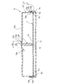
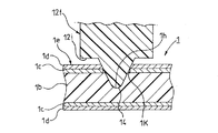
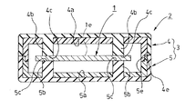
従来の基板収納ケース構造として、図13に示すようなものが知られている(例えば、特許文献1等参照)。 A conventional substrate storage case structure as shown in FIG. 13 is known (see, for example, Patent Document 1).
まず、構成から説明すると、このような従来の基板収納ケース構造では、車両に搭載されて、基板としての電子回路基板1を収納する収納ケース2が、主に上側ケース4及び下側ケース5を嵌め合わせて構成される筐体3を有して構成されている。
First, in terms of configuration, in such a conventional substrate storage case structure, a
また、前記上側ケース4の内側面4aからは、取付リブ部4b,4bが一体に突設されている。
Further, from the
更に、前記下側ケース5の内側面5aからは、取付リブ部5b,5bが一体に突設されている。
Further, from the
そして、これらの、前記上,下側ケース4,5の内側面4a,5aには、合成樹脂製の硬質層4d,5dが設けられていて、周縁部4e,5e同士を嵌合可能としている。
The
次に、この従来の基板収納ケース構造では、この筐体3内に、電子回路基板1が収納される際に、前記下側ケース5の内側面5aから一体に突設された前記取付リブ部5b,5bの上端面5c,5cに、前記電子回路基板1が載置されると共に、前記上側ケース4の内側面4aから一体に突設された取付リブ部4b,4bの下端縁4c,4cが、この電子回路基板1の上面1eに当接されることにより、前記下側ケース5方向に、この電子回路基板1が押さえ付けられて固定される。
Next, in this conventional board storage case structure, when the
このため、前記電子回路基板1を振動等によっても、ガタ付かせることなく、筐体3内に、保持出来る。
For this reason, the
また、合成樹脂製の硬質層4d,5dが、前記上,下側ケース4,5の内側面4a,5aに、設けられているので、前記上,下側ケース4,5の外側の表皮部分をエラストマ等の弾性を有する合成樹脂製材料によって構成できる。
しかしながら、このような基板収納ケース構造では、上側ケース4の内側面4aから一体に突設される取付リブ部4b,4bの下端縁4c,4cの位置寸法及び、前記下側ケース5の内側面5aから一体に突設される取付リブ部5b,5bの上端面5c,5cの位置寸法の交差が厳しく設定されている。
However, in such a substrate storage case structure, the position dimensions of the lower end edges 4c and 4c of the
このため、前記電子回路基板1を振動等によっても、ガタ付かせることなく、保持出来るが、このような公差管理は、寸法精度を常に良好にする必要があると共に、電子回路基板1の板厚公差にも影響を受けてしまうので、製造コストが増大してしまう虞があった。
For this reason, the
しかも、前記従来の収納ケース2では、前記取付リブ部4b,5bを、前記上,下側ケース4,5の外側に2層構造とすることにより設けられる表皮部分のエラストマ等の弾性を有する合成樹脂製材料と同一材料にすることによって、一定の弾性反力を得るようにしている。
Moreover, in the
このため、構造が複雑となり、異なる合成樹脂製材料の2層構造を形成するためには、製造コストが更に、増大してしまう虞があった。 For this reason, the structure becomes complicated, and in order to form a two-layer structure of different synthetic resin materials, there is a possibility that the manufacturing cost further increases.
そこで、この発明は、簡便な構造で、製造コストの増大を抑制しつつ、公差管理を容易とすることが出来る基板収納ケース構造を提供することを目的としている。 Therefore, an object of the present invention is to provide a substrate storage case structure that can easily manage tolerances while suppressing an increase in manufacturing cost with a simple structure.
前記目的を達成するために、請求項1記載の発明は、上側ケース及び下側ケースを嵌め合わせて筐体を構成すると共に、該筐体内には、基板が収納される際に、少なくとも、前記上側ケースから筐体内側に向けて一体に延設されて下端縁を該基板に当接させることにより、前記下側ケース方向側に、該基板を押さえ付けて固定する取付リブ部を有する基板収納ケース構造であって、前記取付リブ部の前記上側ケースへの接続部分に、該取付リブ部を面内外方向への移動を許容して弾性支持する寸法吸収部を設けた基板収納ケース構造を特徴としている。 In order to achieve the above object, according to the first aspect of the present invention, an upper case and a lower case are fitted together to form a casing, and at least when the substrate is stored in the casing, A substrate housing having a mounting rib portion that is integrally extended from the upper case toward the inside of the housing and has a lower end edge in contact with the substrate to press and fix the substrate on the lower case direction side. A case structure comprising a substrate storage case structure in which a dimension absorbing portion that elastically supports the mounting rib portion by allowing movement in the in-plane direction is provided at a connection portion of the mounting rib portion to the upper case. It is said.
また、請求項2に記載されたものは、前記寸法吸収部は、前記上側ケース上面部のうち、前記取付リブ部の周縁を薄肉状とする周縁薄肉弾性部を有して形成されている請求項1記載の基板収納ケース構造を特徴としている。
Further, in the present invention, the dimension absorbing portion is formed so as to have a peripheral thin-walled elastic portion that has a thin peripheral edge of the mounting rib portion in the upper case upper surface portion. The board storage case structure according to
更に、請求項3に記載されたものは、前記取付リブ部の下端縁と、前記基板の上面との間には、前記基板の上面に対して当接する位置を保持する当接位置保持部が設けられている請求項1又は2記載の基板収納ケース構造を特徴としている。
Further, according to a third aspect of the present invention, there is a contact position holding portion that holds a position that contacts the upper surface of the substrate between the lower end edge of the mounting rib portion and the upper surface of the substrate. The board storage case structure according to
このように構成された請求項1記載のものは、前記寸法吸収部が、上側ケースの面内外方向に弾性変形して、寸法誤差を吸収する。 According to the first aspect of the present invention configured as described above, the dimension absorbing portion is elastically deformed in the in-plane direction of the upper case to absorb the dimension error.
この際、前記当接リブ部の下端縁は、前記基板に対して、一定の押さえ力で当接される。 At this time, the lower end edge of the abutment rib portion is abutted against the substrate with a constant pressing force.
このため、振動が、該筐体に作用しても、前記基板が、ガタ付く虞が低減される。 For this reason, even if vibration acts on the housing, the possibility that the substrate is loose is reduced.
また、請求項2に記載されたものは、前記寸法吸収部である周縁薄肉弾性部が、前記上側ケース上面部のうち、前記取付リブ部の周縁を薄肉状として形成されている。 According to a second aspect of the present invention, the peripheral thin-walled elastic portion, which is the dimension absorbing portion, is formed so that the peripheral edge of the mounting rib portion is thin in the upper case upper surface portion.
このため、構成が簡便で、従来のように、異なる材質の2層成型品とするものに比して、例えば、1種類の合成樹脂製素材によって、構成することもできるので、製造コストの上昇を抑制出来る。 For this reason, since the structure is simple and it can be configured with, for example, one type of synthetic resin material as compared with a conventional two-layer molded product made of different materials, the manufacturing cost is increased. Can be suppressed.
更に、請求項3に記載されたものは、前記取付リブ部の下端縁と、前記基板の上面との間で、前記当接位置保持部が、前記基板の上面に対して当接する位置を保持する。 Further, according to a third aspect of the present invention, the position where the contact position holding portion comes into contact with the upper surface of the substrate is held between the lower end edge of the mounting rib portion and the upper surface of the substrate. To do.
このため、前記取付リブ部が、前記上側ケース及び下側ケースを嵌め合わせて筐体を構成する際にも、前記基板に想定されていない角度で干渉して、変形等をする虞も無い。 For this reason, even when the mounting rib portion fits the upper case and the lower case to form a housing, there is no possibility that the mounting rib portion interferes with the substrate at an angle not assumed and is deformed.
従って、常に、所望の同一当接位置を維持出来、前記基板をガタ付かせることなく、該筐体内に保持させることができる。 Therefore, it is possible to always maintain a desired same contact position and hold the substrate in the housing without rattling.
以下、本発明の最良の実施の形態について図面を参照して説明する。 The best mode for carrying out the present invention will be described below with reference to the drawings.
なお、前記従来例と同一乃至均等な部分については、同一符号を付して説明する。 The same or equivalent parts as those in the conventional example will be described with the same reference numerals.
図1乃至図3は、本実施の形態による基板収納ケース構造を示している。 1 to 3 show a substrate storage case structure according to the present embodiment.
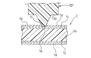
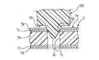
まず、図1を用いて、この基板収納ケース構造の構成から説明すると、このような実施の形態の基板収納ケース構造では、車両に搭載されて、基板としての電子回路基板1を収納する収納ケース10が、上側ケース12の周縁部12aに対向する下側ケース13の周縁部13aの内側に、内嵌させるように、嵌め合わせて構成される筐体11を有して、主に構成されている。
First, the configuration of the substrate storage case structure will be described with reference to FIG. 1. In the substrate storage case structure of such an embodiment, a storage case that is mounted on a vehicle and stores an
このうち、前記周縁部12aの下端縁近傍外側面には、複数の係止爪部12b…が、間隔をおいて、各々外側に向けて一体に突設されている。
Among these, a plurality of locking
また、前記周縁部13aには、この係止爪部12bを、内嵌状態で係止する複数の係止孔部13b…が、開口方向をこの周縁部13aの面内外方向に向けて形成されている。
Further, a plurality of
更に、この実施の形態の基板収納ケース構造では、前記周縁部13a内側には、前記電子回路基板1の外周縁部1aを略全周に渡り載置する段部13cが形成されている。
Furthermore, in the substrate storage case structure of this embodiment, a
そして、この段部13cによって、前記上側ケース12の周縁部12aの下端縁12cとの間に、この電子回路基板1の前記外周縁部1aが、上下方向から挟持されるように構成されている。
The
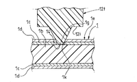
この電子回路基板1は、図2に示すように、樹脂製の基板面部1bの上,下両側面側に、必要に応じて、導電体としての銅箔層1c,1cが設けられると共に、必要に応じて、これらの各銅箔層1c,1cの上にレジスト層1d,1dが形成されて、概略構成されている。
As shown in FIG. 2, the
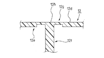
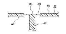
更に、この実施の形態では、前記上側ケース12の上面部12dには、内側面12eの略中央位置から下方である筐体11内部空間方向に向けて、円柱状の取付リブ部12fが、前記電子回路基板1に対して垂直となるように、一体に突設されている。
Furthermore, in this embodiment, a cylindrical
この取付リブ部12fの前記上側ケース12の上面部12dへの接続部分には、上面視円形の寸法吸収部としての周縁薄肉弾性部12gが設けられている。
A peripheral thin-walled elastic portion 12g serving as a dimension-absorbing portion having a circular shape in a top view is provided at a connection portion of the
この周縁薄肉弾性部12gは、前記取付リブ部12fの基端部12hの周縁を薄肉状とすることにより、面内外方向への移動を許容して弾性支持している。
The peripheral thin-walled elastic portion 12g is elastically supported by allowing movement in the in-plane and outward directions by making the peripheral edge of the
そして、この周縁薄肉弾性部12gは、前記上側ケース12の上面部12dの他の部分の板厚の約2/3〜1/20の厚みを有していて、前記取付リブ部12fの外形寸法d1の約3倍〜約5倍程度の外形寸法d2を呈して、この基端部12hの全周に一定の幅で、円環状を呈するように形成されている。
The peripheral thin elastic portion 12g has a thickness of about 2/3 to 1/20 of the thickness of the other portion of the
また、この実施の形態では、前記取付リブ部12fの下端縁12iには、前記電子回路基板1の上面1eに対して当接する位置を保持するように、突設形成される当接位置保持部としての突起部14が、一体となるように設けられている。
In this embodiment, the abutment position holding portion is formed so as to protrude from the
この実施の形態では、図2に示すように、当接によって、前記基板面部1bの上側面側に形成された各銅箔層1cの上のレジスト層1dに、前記突起部14が、当接により、一定深さまで入り込んで、凹部1fが形成されるように構成されている。
In this embodiment, as shown in FIG. 2, the
次に、この実施の形態の基板収納ケース構造の作用について説明する。 Next, the operation of the substrate storage case structure of this embodiment will be described.
この実施の形態の基板収納ケース構造では、まず、前記下側ケース13の前記周縁部13a内側に略全周に渡り形成された段部13cに、前記電子回路基板1の外周縁部1aを上方から係止させるように載置する。
In the substrate storage case structure of this embodiment, first, the outer
次に、前記上側ケース12の周縁部12aを、下側ケース13の周縁部13aに対向させて、この下側ケース13の周縁部13a内側に、この周縁部12aを、内嵌させるように、嵌め合わせる。
Next, the
この際、前記周縁部12aの下端縁近傍外側面に形成された各係止爪部12b…が、前記周縁部13aに、開口形成された複数の係止孔部13b…に各々係止されて、この内嵌状態で固定される。
At this time, the
そして、前記取付リブ部12fの下端縁12iに形成された突起部14の下端が、前記基板1の上面1eに当接すると、前記周縁薄肉弾性部12gが、図1中二点鎖線に示す位置若しくは、図3中に示す位置から、図1中実線に示すように、上側ケース12の上面部12dの面内外方向に弾性変形して、寸法誤差が吸収される。
When the lower end of the
また、この際、前記当接リブ部14の下端縁は、前記基板1に対して、一定の押さえ力で当接されている。
At this time, the lower end edge of the
このため、振動が、この筐体10に作用しても、前記基板1が、筐体10内部でガタ付く虞が低減される。
For this reason, even if vibration acts on the
このように、簡便な構成で、上,下側ケース12,13及び電子回路基板1の寸法誤差を吸収させて、この電子回路基板1をガタ付かせることなく、筐体10内部に保持できるので、各部品の寸法公差を余り厳しく設定しなくてもよい。
In this way, with a simple configuration, the dimensional errors of the upper and
従って、容易な公差管理で、しかも、製造コストの増大を抑制することができる。 Therefore, an increase in manufacturing cost can be suppressed with easy tolerance management.
更に、この実施の形態では、前記寸法吸収部である周縁薄肉弾性部12gが、前記上側ケース12の上面部12dのうち、前記取付リブ部12fの基端部12hの周縁を薄肉状として形成されている。
Further, in this embodiment, the peripheral thin elastic portion 12g which is the dimension absorbing portion is formed so that the peripheral edge of the
このため、構成が簡便で、例えば、1種類の合成樹脂製素材によって、射出成形等を行うことにより、構成することもできる。 For this reason, a structure is simple and can also be comprised by performing injection molding etc. with one type of synthetic resin raw materials, for example.
従って、従来のように、異なる材質の2層成型品によって構成されるものに比して、比較的安価に製造出来、製造コストの上昇を抑制出来る。 Therefore, it can be manufactured at a relatively low cost as compared with the conventional one formed by a two-layer molded product of different materials, and an increase in manufacturing cost can be suppressed.
更に、この実施の形態では、図2に示すように、前記取付リブ部12fの下端縁12iに設けられた突起部14が、前記基板1の上面1eに塗布されたレジスト層1dの一部内まで、入り込んで、摩擦力を増大させることにより、基板1の上面1eに対して当接する位置が保持される。
Further, in this embodiment, as shown in FIG. 2, the
このため、前記取付リブ部12fが、前記上側ケース12及び下側ケース13を嵌め合わせて筐体11が構成される際にも、前記基板1に想定されていない直交しない角度で干渉して、倒れたり或いは屈曲される等の変形等をする虞も無い。
For this reason, when the housing 11 is configured by fitting the
従って、常に、所望の同一当接位置を維持出来、前記基板1をガタ付かせることなく、この筐体10内に保持させることができる。
Therefore, it is possible to always maintain a desired identical contact position and hold the
また、この実施の形態では、前記取付リブ部12fの下端縁12iに設けられた突起部14が、先端の小さな面積で、前記電子回路基板1の上面1eに当接される。
In this embodiment, the
このため、電子回路基板1の上面1eの電子部品の配置や、回路パターンの設定可能面積が増大して、電子回路基板1の設計の自由度が増大する。
For this reason, the arrangement of the electronic components on the
しかも、この実施の形態では、前記円柱状の取付リブ部12fが、前記上側ケース12の上面部12dには、内側面12eの略中央位置から下方である筐体11内部空間方向に向けて、1本形成されているのみであるので、更に、突起部14が、前記電子回路基板1の上面1eに当接される面積を減少させることができる。
In addition, in this embodiment, the cylindrical mounting
この際にも、前記突起部14が、前記基板面部1bの上側面側に形成された各銅箔層1cの上のレジスト層1dに、一定深さまで入り込んで、凹部1fが形成されて、摩擦抵抗係数を増大させるので、前記周縁薄肉弾性部12gの厚みを、弾性変形可能な薄さ(この実施の形態では、前記上側ケース12の上面部12dの他の部分の板厚の約2/3〜1/20の厚み)としても、転倒や屈曲等によって破断等、損傷する虞が減少されている。
Also at this time, the
図4は、この発明の実施の形態の実施例1の基板収納ケース構造を示すものである。 FIG. 4 shows a substrate storage case structure according to Example 1 of the embodiment of the present invention.
なお、前記実施の形態と同一乃至均等な部分については、前記実施の形態と同一符号を付して説明する。 Note that portions that are the same as or equivalent to those in the above-described embodiment are described with the same reference numerals as those in the above-described embodiment.
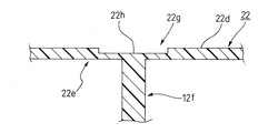
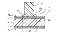
まず、構成から説明すると、この実施例1の上側ケース22では、前記取付リブ部12fの前記上側ケース22の上面部22dへの接続部分であり、基端部22hの周縁には、上面視円形の寸法吸収部としての周縁薄肉弾性部22gが設けられている。
First, in terms of configuration, in the
この周縁薄肉弾性部22gは、前記取付リブ部12fの基端部22hの周縁を、前記上面部22dの上側を凹状として薄肉状とすることにより、面内外方向への移動を許容して、この取付リブ部12fを弾性支持するように構成されている。
This peripheral thin-walled
次に、この実施例1の基板収納ケース構造の作用について説明する。 Next, the operation of the substrate storage case structure of the first embodiment will be described.
このように構成された実施例1の基板収納ケース構造では、前記取付リブ部12f下端縁の前記基板1の上面1eへの当接により、前記基端部22hが、面内外方向で、上方に移動しても、他の上面部22dの外表面位置から、前記周縁薄肉弾性部22gが上方に突出しないように、或いは突出量を少なく設定出来る。
In the substrate storage case structure of the first embodiment configured as described above, the
他の構成及び作用効果については、前記実施の形態と略同様であるので、説明を省略する。 Other configurations and operational effects are substantially the same as those of the above-described embodiment, and thus description thereof is omitted.
図5は、この発明の実施の形態の実施例2の基板収納ケース構造を示すものである。 FIG. 5 shows a substrate storage case structure according to Example 2 of the embodiment of the present invention.
なお、前記実施の形態及び実施例1と同一乃至均等な部分については、前記実施の形態及び実施例1と同一符号を付して説明する。 The same or equivalent parts as those in the above embodiment and example 1 will be described with the same reference numerals as those in the above embodiment and example 1.
まず、構成から説明すると、この実施例2の基板収納ケース構造では、上側ケース32のうち、前記取付リブ部12fの前記上側ケース32の上面部32dへの接続部分であり基端部32hの周縁には、上面視円形の寸法吸収部としての周縁薄肉弾性部32gが設けられている。
First, in terms of configuration, in the substrate storage case structure of the second embodiment, in the
この周縁薄肉弾性部32gは、前記取付リブ部12fの基端部32hの周縁を、前記上面部32dの上,下側を各々凹状として薄肉状とすることにより、面内外方向への移動を許容して、この取付リブ部12fを弾性支持するように構成されている。
The peripheral thin
他の構成及び作用効果については、前記実施の形態及び実施例1と略同様であるので、説明を省略する。 Other configurations and operational effects are substantially the same as those of the above-described embodiment and Example 1, and thus description thereof is omitted.
図6は、この発明の実施の形態の実施例3の基板収納ケース構造を示すものである。
なお、前記実施の形態及び実施例1,2と同一乃至均等な部分については、前記実施の形態及び実施例1,2と同一符号を付して説明する。
FIG. 6 shows a substrate storage case structure according to Example 3 of the embodiment of the present invention.
Parts that are the same as or equivalent to those in the embodiment and Examples 1 and 2 are described using the same reference numerals as those in the embodiment and Examples 1 and 2.
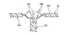
まず、構成から説明すると、この実施例3の基板収納ケース構造では、上側ケース42のうち、前記取付リブ部12fの前記上側ケース42の上面部42dへの接続部分であり基端部42hの周縁には、上面視円形の寸法吸収部としての周縁薄肉弾性部42gが設けられている。
First, in terms of configuration, in the substrate storage case structure of the third embodiment, in the
この周縁薄肉弾性部42gは、前記取付リブ部12fの基端部42hの周縁を、前記上面部42dの上,下側を各々凹状として薄肉状とすると共に、通常状態では、図6中実線で示す位置まで、前記基端部42hを下方にオフセットすることにより、図6中二点鎖線に示す位置まで、面内外方向への移動を許容して、白抜き矢印に示すようなストローク量を確保して、この取付リブ部12fを弾性支持するように構成されている。
The peripheral thin-walled elastic portion 42g has a thin peripheral shape with the peripheral edge of the
次に、この実施例3の基板収納ケース構造の作用について説明する。 Next, the operation of the substrate storage case structure of the third embodiment will be described.
通常状態では、図6中実線で示す位置まで、前記基端部42hが、下方にオフセットされている。
In the normal state, the
このため、前記取付リブ部12f下端縁の前記基板1の上面1eへの当接により、前記基端部42hが、面内外方向で、上方に移動する際、図6中二点鎖線に示す位置まで、面内外方向への移動が許容されて、白抜き矢印に示すようなストローク量を充分に確保出来る。
For this reason, when the
他の構成、及び作用効果については、前記実施の形態及び実施例1,2と略同一であるので、説明を省略する。 Other configurations and functions and effects are substantially the same as those of the above-described embodiment and Examples 1 and 2, and thus description thereof is omitted.
図7は、この発明の実施の形態の実施例4の基板収納ケース構造を示すものである。
なお、前記実施の形態及び実施例1乃至3と同一乃至均等な部分については、前記実施の形態及び実施例1乃至3と同一符号を付して説明する。
FIG. 7 shows a substrate storage case structure according to Example 4 of the embodiment of the present invention.
The same or equivalent parts as those of the embodiment and Examples 1 to 3 will be described with the same reference numerals as those of the embodiment and Examples 1 to 3.
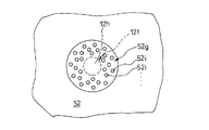
まず、構成から説明すると、この実施例4の基板収納ケース構造では、上側ケース52と、前記取付リブ部12fの基端部12hとの接続部分であり、基端部12hの周縁には、上面視円形の寸法吸収部としての肉抜き部52gが設けられている。
First, in terms of configuration, in the substrate storage case structure of the fourth embodiment, it is a connection portion between the
この肉抜き部52gには、複数の開孔部52i…が、面内外方向を貫通するように開口形成されていて、弾性変形可能とすることにより、この上側ケース52の面内外方向への移動することが許容されて、この取付リブ部12fが、弾性支持されている。
A plurality of
次に、この実施例4の基板収納ケース構造の作用について説明する。 Next, the operation of the substrate storage case structure of the fourth embodiment will be described.
この実施例4の基板収納ケース構造では、前記取付リブ部12f下端縁が、前記基板1の上面1eへ当接すると、前記複数の開孔部52i…を、面内外方向へ貫通するように開口形成した前記肉抜き部52gが、面内外方向へ弾性変形しながら、前記基端部12hを上方へ移動させる。
In the substrate storage case structure of the fourth embodiment, when the lower end edge of the mounting
他の構成、及び作用効果については、前記実施の形態及び実施例1乃至3と略同一であるので、説明を省略する。 Other configurations and operational effects are substantially the same as those in the above-described embodiment and Examples 1 to 3, and thus the description thereof is omitted.
図8は、この発明の実施の形態の実施例5の基板収納ケース構造を示すものである。 FIG. 8 shows a substrate storage case structure according to Example 5 of the embodiment of the present invention.
なお、前記実施の形態及び実施例1乃至4と同一乃至均等な部分については、前記実施の形態及び実施例1乃至4と同一符号を付して説明する。 The same or equivalent parts as those of the embodiment and Examples 1 to 4 will be described with the same reference numerals as those of the embodiment and Examples 1 to 4.
まず、構成から説明すると、この実施例5の基板収納ケース構造では、前記基板面部1bの上側面側に形成された銅箔層1cの一部に、前記取付リブ部12fの突起部14を挿通する開口1kが形成されていて、当接位置保持部としての一方の凹部1gを構成している。
First, in terms of configuration, in the substrate storage case structure of the fifth embodiment, the protruding
次に、この実施例5の基板収納ケース構造の作用について説明する。 Next, the operation of the substrate storage case structure of the fifth embodiment will be described.
この実施例5では、前記基板1の上面1eに形成された凹部1g内に、前記取付リブ部12fの突起部14が突入されると、一定量、前記突起部14が、この凹部1g内に挿入された状態で開口周縁に係止される。
In the fifth embodiment, when the
このため、更に、外れにくく、前記所望の位置に前記取付リブ部12fを固定出来る。
For this reason, it is further difficult to come off, and the mounting
他の構成、及び作用効果については、前記実施の形態及び実施例1乃至4と略同一であるので、説明を省略する。 Other configurations and functions and effects are substantially the same as those of the above-described embodiment and Examples 1 to 4, and thus description thereof is omitted.
図9は、この発明の実施の形態の実施例6の基板収納ケース構造を示すものである。 FIG. 9 shows a substrate storage case structure according to Example 6 of the embodiment of the present invention.
なお、前記実施の形態及び実施例1乃至5と同一乃至均等な部分については、前記実施の形態及び実施例1乃至5と同一符号を付して説明する。 The same or equivalent parts as those of the embodiment and Examples 1 to 5 will be described with the same reference numerals as those of the embodiment and Examples 1 to 5.
まず、構成から説明すると、この実施例6の基板収納ケース構造では、前記基板1の基板面部1bの上側面側で、前記基板面部1bの一部に、前記取付リブ部12fの突起部14を没入させる当接位置保持部としての凹部1hが、凹設形成されている。
First, in terms of configuration, in the substrate storage case structure of the sixth embodiment, the
次に、この実施例6の基板収納ケース構造の作用について説明する。 Next, the operation of the substrate storage case structure of the sixth embodiment will be described.
この実施例6では、前記基板1の基板面部1bに形成された凹部1h内に、前記取付リブ部12fの突起部14が没入されると、一定量、前記突起部14が、この凹部1h内に挿入された状態で係止される。
In the sixth embodiment, when the
このため、更に、外れにくく、前記所望の位置に前記取付リブ部12fを固定出来る。
For this reason, it is further difficult to come off, and the mounting
他の構成、及び作用効果については、前記実施の形態及び実施例1乃至4と略同一であるので、説明を省略する。 Other configurations and functions and effects are substantially the same as those of the above-described embodiment and Examples 1 to 4, and thus description thereof is omitted.
図10は、この発明の実施の形態の実施例7の基板収納ケース構造を示すものである。 FIG. 10 shows a substrate storage case structure according to Example 7 of the embodiment of the present invention.
なお、前記実施の形態及び実施例1乃至6と同一乃至均等な部分については、前記実施の形態及び実施例1乃至6と同一符号を付して説明する。 The same or equivalent parts as those of the embodiment and Examples 1 to 6 will be described with the same reference numerals as those of the embodiment and Examples 1 to 6.
まず、構成から説明すると、この実施例7の基板収納ケース構造では、前記基板1の基板面部1bに、前記取付リブ部12fの突起部14を没入させる当接位置保持部としての挿通孔1iが、面内外方向に貫通するように開口形成されている。
First, in terms of configuration, in the substrate storage case structure of the seventh embodiment, an
次に、この実施例7の基板収納ケース構造の作用について説明する。 Next, the operation of the substrate storage case structure of the seventh embodiment will be described.
この実施例7では、前記基板1の基板面部1bに形成された挿通孔1i内に、前記取付リブ部12fの突起部14が没入されると、一定量、前記突起部14が、この挿通孔1i内に挿入された状態で係止される。
In the seventh embodiment, when the
このため、更に、外れにくく、前記所望の位置に前記取付リブ部12fを固定出来る。
For this reason, it is further difficult to come off, and the mounting
他の構成、及び作用効果については、前記実施の形態及び実施例1乃至6と略同一であるので、説明を省略する。 Other configurations and functions and effects are substantially the same as those of the above-described embodiment and Examples 1 to 6, and thus description thereof is omitted.
図11は、この発明の実施の形態の実施例8の基板収納ケース構造を示すものである。 FIG. 11 shows a substrate storage case structure according to Example 8 of the embodiment of the present invention.
なお、前記実施の形態及び実施例1乃至7と同一乃至均等な部分については、前記実施の形態及び実施例1乃至7と同一符号を付して説明する。 The same or equivalent parts as those of the embodiment and Examples 1 to 7 will be described with the same reference numerals as those of the embodiment and Examples 1 to 7.
まず、構成から説明すると、この実施例8の基板収納ケース構造では、前記取付リブ部22fの下端縁22iには、当接位置保持部としてのフランジ部22gが、外径寸法d3を、前記実施の形態の取付リブ部12fの外形寸法d1よりも大きく設定して形成されている。
First, in terms of configuration, in the substrate storage case structure of the eighth embodiment, a
そして、比較的大きな当接面積を有する下端面22jが、この取付リブ部22fの下端縁22iに略水平に形成されている。
A
次に、この実施例8の基板収納ケース構造の作用について説明する。 Next, the operation of the substrate storage case structure of the eighth embodiment will be described.
この実施例8では、比較的大きな当接面積を有する下端面部22iが、前記基板1の上面1eに当接して、安定する。
In the eighth embodiment, the lower
このため、基板1に想定されていない角度で干渉して、変形等をする虞が無く、しかも、外れにいので、前記所望の位置に前記取付リブ部22fを固定出来る。
For this reason, there is no possibility that the
他の構成、及び作用効果については、前記実施の形態及び実施例1乃至7と略同一であるので、説明を省略する。 Other configurations and functions and effects are substantially the same as those of the above-described embodiment and Examples 1 to 7, and thus description thereof is omitted.
図12は、この発明の実施の形態の実施例9の基板収納ケース構造を示すものである。 FIG. 12 shows a substrate storage case structure according to Example 9 of the embodiment of the present invention.
なお、前記実施の形態及び実施例1乃至8と同一乃至均等な部分については、前記実施の形態及び実施例1乃至8と同一符号を付して説明する。 The same or equivalent parts as those of the embodiment and Examples 1 to 8 will be described with the same reference numerals as those of the embodiment and Examples 1 to 8.
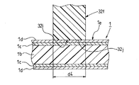
まず、構成から説明すると、この実施例9の基板収納ケース構造では、前記取付リブ部32fが、上,下方向に略一定寸法の外径寸法を有して構成されていると共に、この取付リブ部32fの下端縁32iには、当接位置保持部として、前記実施例8のフランジ部22gの外径寸法d3と、略同一寸法となる外形寸法d4を有する下端面32jが設けられている。
First, in terms of configuration, in the substrate storage case structure of the ninth embodiment, the mounting
そして、比較的大きな当接面積を有する下端面32jが、前記基板1の上面1eに当接するように構成されている。
A
次に、この実施例9の基板収納ケース構造の作用について説明する。 Next, the operation of the substrate storage case structure of the ninth embodiment will be described.
この実施例9では、比較的大きな当接面積を有する下端面32jが、前記基板1の上面1eに当接して、安定する。
In the ninth embodiment, the
このため、基板1に想定されていない角度で干渉して、変形等をする虞が無く、しかも、外れにいので、前記所望の位置に前記取付リブ部32fを固定出来る。
For this reason, there is no possibility that the
他の構成、及び作用効果については、前記実施の形態及び実施例1乃至8と略同一であるので、説明を省略する。 Other configurations and functions and effects are substantially the same as those of the above-described embodiment and Examples 1 to 8, and thus description thereof is omitted.
以上、図面を参照して、本発明の最良の実施の形態及び実施例1乃至9を詳述してきたが、具体的な構成は、この実施の形態及び実施例1乃至9に限らず、本発明の要旨を逸脱しない程度の設計的変更は、本発明に含まれる。 The best embodiment and Examples 1 to 9 of the present invention have been described in detail with reference to the drawings. However, the specific configuration is not limited to this embodiment and Examples 1 to 9, and the present embodiment is not limited to this. Design changes that do not depart from the gist of the invention are included in the present invention.
例えば、前記実施の形態では、図2に示すように、前記取付リブ部12fの下端縁12iに設けられた突起部14が、前記基板1の上面1eに塗布されたレジスト層1dの一部内まで、入り込んで、摩擦力を増大させることにより、基板1の上面1eに対して当接する位置が保持されるように構成されているが、特にこれに限らず、例えば、レジスト層1dが形成されていない部分であっても、前記当接リブ部12fの下端縁が、前記基板1に対して、一定の押さえ力で当接されるものであるならば、どのような形状、数量及び材質で、前記取付リブ部12fの下端縁と、前記基板1の上面1eとの間を当接させるようにしてもよい。
For example, in the embodiment, as shown in FIG. 2, the
1 電子回路基板(基板)
1e 上面
10 収納ケース
11 筐体
12 上側ケース
寸法吸収部
12g,22g,32g,42g 周縁薄肉弾性部
52g 肉抜き部
12f,22f,32f
取付リブ部
13 下側ケース
当接位置保持部
1f,1g,1h 凹部
1i 挿通孔
14 突起部
22j,32j 当接面
1 Electronic circuit board (substrate)
12f, 22f, 32f
Mounting
Claims (3)
前記取付リブ部の前記上側ケースへの接続部分に、該取付リブ部を面内外方向への移動を許容して弾性支持する寸法吸収部を設けたことを特徴とする基板収納ケース構造。 The upper case and the lower case are fitted together to form a housing, and when the board is stored in the housing, at least the lower case is integrally extended from the upper case toward the inside of the housing. A substrate storage case structure having a mounting rib portion that presses and fixes the substrate on the lower case direction side by bringing an edge into contact with the substrate,
A substrate storage case structure, characterized in that a dimension absorbing portion that elastically supports the mounting rib portion while allowing the mounting rib portion to move in an in-plane direction is provided at a connection portion of the mounting rib portion to the upper case.
2. A contact position holding portion that holds a position that makes contact with the upper surface of the substrate is provided between a lower end edge of the mounting rib portion and an upper surface of the substrate. Or the board | substrate storage case structure of 2 description.
Priority Applications (1)
| Application Number | Priority Date | Filing Date | Title |
|---|---|---|---|
| JP2004110843A JP2005294721A (en) | 2004-04-05 | 2004-04-05 | Structure of substrate storing case |
Applications Claiming Priority (1)
| Application Number | Priority Date | Filing Date | Title |
|---|---|---|---|
| JP2004110843A JP2005294721A (en) | 2004-04-05 | 2004-04-05 | Structure of substrate storing case |
Publications (1)
| Publication Number | Publication Date |
|---|---|
| JP2005294721A true JP2005294721A (en) | 2005-10-20 |
Family
ID=35327280
Family Applications (1)
| Application Number | Title | Priority Date | Filing Date |
|---|---|---|---|
| JP2004110843A Pending JP2005294721A (en) | 2004-04-05 | 2004-04-05 | Structure of substrate storing case |
Country Status (1)
| Country | Link |
|---|---|
| JP (1) | JP2005294721A (en) |
Cited By (2)
| Publication number | Priority date | Publication date | Assignee | Title |
|---|---|---|---|---|
| JP2023141146A (en) * | 2022-03-23 | 2023-10-05 | 株式会社デンソー | board housing |
| DE102024108791A1 (en) * | 2024-03-27 | 2025-10-02 | Kiekert Aktiengesellschaft | Housings for automotive applications |
-
2004
- 2004-04-05 JP JP2004110843A patent/JP2005294721A/en active Pending
Cited By (3)
| Publication number | Priority date | Publication date | Assignee | Title |
|---|---|---|---|---|
| JP2023141146A (en) * | 2022-03-23 | 2023-10-05 | 株式会社デンソー | board housing |
| DE102024108791A1 (en) * | 2024-03-27 | 2025-10-02 | Kiekert Aktiengesellschaft | Housings for automotive applications |
| WO2025201595A1 (en) * | 2024-03-27 | 2025-10-02 | Kiekert Aktiengesellschaft | Casing for automotive applications |
Similar Documents
| Publication | Publication Date | Title |
|---|---|---|
| JP4379288B2 (en) | Electronic device housing structure | |
| JP4365426B2 (en) | Meter device | |
| JP6562277B2 (en) | Case and watch | |
| CN103098569A (en) | Circuit housing having a printed circuit board which is positioned in said circuit housing by means of positioning elements | |
| JPH1070381A (en) | Wiring board fixing structure | |
| JP2019029873A (en) | Antenna device | |
| JP2005294721A (en) | Structure of substrate storing case | |
| JP7384618B2 (en) | Connection structure and assembly | |
| US20090123017A1 (en) | Electronic component, electronic component unit, speaker, and mobile terminal including speaker | |
| JP2005142215A (en) | Deformation prevention structure of housing lid | |
| JP2791295B2 (en) | Substrate holding structure | |
| JP2009076414A (en) | Push button switch | |
| JP4586848B2 (en) | Resin case and electronic device | |
| JP2009016086A (en) | Operation member | |
| JP2007005103A (en) | How to attach the key top to the press switch, and the press switch | |
| JP7085965B2 (en) | Switch module and switch device | |
| JP2002025382A (en) | Cover member for push-button switch | |
| JP2002223079A (en) | Printed circuit board housing case for electronic equipment and printed circuit board mounting method | |
| JP2008305694A (en) | Holding structure of rubber key for switch operation of portable electronic equipment | |
| JP2011210403A (en) | Pressing type electronic component | |
| JP6102968B2 (en) | Keyboard device | |
| JP7508385B2 (en) | Anchor structure and harness protection equipment | |
| JP2007093873A (en) | Camera module mounting structure and information terminal device including the same | |
| JP5743839B2 (en) | Push button structure | |
| JP3748187B2 (en) | Switch mechanism |