JP2005294587A - Method for forming charge transport layer, organic semiconductor structure and method for producing the same - Google Patents
Method for forming charge transport layer, organic semiconductor structure and method for producing the same Download PDFInfo
- Publication number
- JP2005294587A JP2005294587A JP2004108527A JP2004108527A JP2005294587A JP 2005294587 A JP2005294587 A JP 2005294587A JP 2004108527 A JP2004108527 A JP 2004108527A JP 2004108527 A JP2004108527 A JP 2004108527A JP 2005294587 A JP2005294587 A JP 2005294587A
- Authority
- JP
- Japan
- Prior art keywords
- charge transport
- transport layer
- organic semiconductor
- semiconductor structure
- hole transport
- Prior art date
- Legal status (The legal status is an assumption and is not a legal conclusion. Google has not performed a legal analysis and makes no representation as to the accuracy of the status listed.)
- Withdrawn
Links
Images


Landscapes
- Electroluminescent Light Sources (AREA)
- Thin Film Transistor (AREA)
Abstract
Description
本発明は、両極性を有する電荷輸送層の形成方法並びに電荷輸送層を備えた有機半導体構造物及びその製造方法に関するものである。 The present invention relates to a method for forming a charge transport layer having both polarities, an organic semiconductor structure provided with the charge transport layer, and a method for producing the same.
近年、電荷輸送能を有する材料を用いた各種の有機デバイスについての研究が注目され、特にフレキシブルディスプレイ装置等に利用可能な薄膜トランジスタ(有機TFTともいう。)、有機EL素子、太陽電池等、各方面への応用が期待されている。そうした各種の有機デバイスのうち、例えば有機EL素子においては、発光層、正孔輸送層、電子輸送層等からなる電荷輸送能を有した各種の機能層を備えている。 In recent years, research on various organic devices using a material having a charge transporting ability has attracted attention, and in particular, thin film transistors (also referred to as organic TFTs), organic EL elements, solar cells, etc. that can be used for flexible display devices and the like. Application to is expected. Among such various organic devices, for example, an organic EL element includes various functional layers having a charge transporting capability including a light emitting layer, a hole transport layer, an electron transport layer, and the like.
有機EL素子や有機TFT等に形成される上記の機能層は、使用する材料の分子量や性質に応じて、真空蒸着や塗布法等によって成膜されている(例えば、非特許文献1及び2を参照)。
本発明者らは、電荷輸送能を有する各種の有機半導体材料について多方面から研究している過程で、正孔輸送能を有し、電子輸送能は有さない有機半導体材料として従来から認知されているものであっても、その取り扱いによっては電子輸送能を有する両極性の電荷輸送層となることを見出して本発明を完成させた。 In the process of studying various organic semiconductor materials having charge transporting ability from various fields, the present inventors have been conventionally recognized as organic semiconductor materials having hole transporting ability and not having electron transporting ability. The present invention has been completed by finding that it can be a bipolar charge transport layer having an electron transport ability depending on its handling.
したがって、本発明は、こうした知見に基づいてなされたものであって、その目的は、両極性を有する電荷輸送層の新たな形成方法並びに電荷輸送層を備えた有機半導体構造物及びその製造方法を提供することにある。 Accordingly, the present invention has been made on the basis of such knowledge, and its object is to provide a new method for forming a charge transport layer having both polarities, an organic semiconductor structure having a charge transport layer, and a method for producing the same. It is to provide.
上記目的を達成する本発明の電荷輸送層の形成方法は、流動性を有する正孔輸送材料を予め形成された空隙内に酸素遮断手段を利用して注入することにより、両極性の電荷輸送層を形成することを特徴とする。 The method for forming a charge transport layer of the present invention that achieves the above-described object is achieved by injecting a hole transport material having fluidity into a previously formed gap by utilizing an oxygen blocking means, thereby providing a bipolar charge transport layer. It is characterized by forming.
本来的に両極性の電荷輸送能を有する正孔輸送材料でありながら、材料中に混入した酸素で電子がトラップされてあたかも電子輸送能を発現しないと認知されていた材料について、本発明の方法により、両極性を有する電荷輸送層を形成することができる。 The method according to the present invention is a material that has been recognized as an electron transporting ability as though it was originally a hole transporting material having an ambipolar charge transporting ability but trapped by oxygen mixed in the material. Thus, a charge transport layer having both polarities can be formed.
本発明の電荷輸送層の形成方法は、上記電荷輸送層の形成方法において、前記酸素遮断手段が毛細管現象を利用した手段であることを特徴とする。この発明によれば、流動性を有する材料を毛細管現象で空隙内に注入する手段を用いるので、電荷輸送層の形成時に流動性を有する材料が大気や酸素含有雰囲気下に曝されるのを防ぐことができる。 The charge transport layer forming method of the present invention is characterized in that, in the above charge transport layer forming method, the oxygen blocking means is a means utilizing a capillary phenomenon. According to the present invention, since a means for injecting a fluid material into the gap by capillary action is used, the fluid material is prevented from being exposed to the atmosphere or an oxygen-containing atmosphere when forming the charge transport layer. be able to.
上記目的を達成する本発明の有機半導体構造物は、予め形成された空隙内に、正孔輸送材料からなる両極性の電荷輸送層が形成されていることを特徴とする。この発明によれば、本来的に両極性の電荷輸送能を有する正孔輸送材料でありながらその材料中に混入した酸素で電子がトラップされてあたかも電子輸送能を発現しないと認知されていた材料を用いて、新規な有機半導体構造物を構成することができる。 The organic semiconductor structure of the present invention that achieves the above object is characterized in that a bipolar charge transport layer made of a hole transport material is formed in a previously formed void. According to the present invention, although it is a hole transport material that originally has a bipolar charge transport capability, it was recognized that electrons were trapped by oxygen mixed in the material as if it did not exhibit the electron transport capability Can be used to form a novel organic semiconductor structure.
本発明の有機半導体構造物は、上記有機半導体構造物において、前記正孔輸送材料が、液晶状態、液体状態又は非晶質状態となり得る材料であることを特徴とする。この発明によれば、正孔輸送材料が液晶状態、液体状態又は非晶質状態となり得る材料の何れであっても構わない。 The organic semiconductor structure of the present invention is characterized in that, in the organic semiconductor structure, the hole transport material is a material that can be in a liquid crystal state, a liquid state, or an amorphous state. According to the present invention, the hole transport material may be any material that can be in a liquid crystal state, a liquid state, or an amorphous state.
上記目的を達成する本発明の有機半導体構造物の製造方法は、一対の基板が所定の間隔を隔てて対向配置されてなる空間内に、流動性を有する正孔輸送材料を酸素を遮断した状態で注入する工程を含むことを特徴とする。この発明によれば、電荷輸送層の形成時に流動性を有する材料が大気や酸素含有雰囲気下に曝されるのを防ぐことができるので、有機半導体構造物に予め設けられた空間内に、本来的に両極性の電荷輸送能を有する正孔輸送材料を用いて実際に両極性を有する電荷輸送層を形成することができる。 In the method for producing an organic semiconductor structure of the present invention that achieves the above object, a hole transport material having fluidity is blocked from oxygen in a space in which a pair of substrates are opposed to each other at a predetermined interval. The method includes a step of injecting at a step. According to the present invention, it is possible to prevent the material having fluidity from being exposed to the air or an oxygen-containing atmosphere when forming the charge transport layer. In particular, a charge transport layer having both polarities can be formed by using a hole transporting material having bipolar charge transporting ability.
以上説明したように、本発明の電荷輸送層の形成方法によれば、本来的に両極性の電荷輸送能を有する正孔輸送材料でありながら、材料中に混入した酸素で電子がトラップされてあたかも電子輸送能を発現しないと認知されていた材料を用いて、両極性を有する電荷輸送層を形成することができる。 As described above, according to the method for forming a charge transport layer of the present invention, electrons are trapped by oxygen mixed in the material while being a hole transport material that inherently has a bipolar charge transport ability. A charge transport layer having both polarities can be formed using a material that has been recognized as not exhibiting electron transport ability.
また、本発明の有機半導体構造物によれば、本来的に両極性の電荷輸送能を有する正孔輸送材料でありながらその材料中に混入した酸素で電子がトラップされてあたかも電子輸送能を発現しないと認知されていた材料を用いて、新規な有機半導体構造物を構成することができる。 In addition, according to the organic semiconductor structure of the present invention, although it is a hole transport material that inherently has a bipolar charge transport capability, electrons are trapped by oxygen mixed in the material, as if the electron transport capability is exhibited. A novel organic semiconductor structure can be constructed using materials that have been recognized as not.
また、本発明の有機半導体構造物の製造方法によれば、電荷輸送層の形成時に流動性を有する材料が大気や酸素含有雰囲気下に曝されるのを防ぐことができるので、有機半導体構造物に予め設けられた空間内に、本来的に両極性の電荷輸送能を有する正孔輸送材料を用いて実際に両極性を有する電荷輸送層を形成することができる。 In addition, according to the method for producing an organic semiconductor structure of the present invention, it is possible to prevent a fluid material from being exposed to the atmosphere or an oxygen-containing atmosphere when forming the charge transport layer. In the space provided in advance, a charge transport layer having an actual polarity can be formed by using a hole transport material having an inherent charge transport capability of both polarities.
本発明の電荷輸送層及び有機半導体構造物は、特にフレキシブルディスプレイ装置等に利用可能な薄膜トランジスタ(有機TFTともいう。)、有機EL素子、太陽電池等、電荷輸送能を有する材料を用いた各種の有機デバイスについて、その適用の幅を一層広げることに寄与できる。 The charge transport layer and the organic semiconductor structure of the present invention are various kinds of materials using charge transporting materials such as thin film transistors (also referred to as organic TFTs), organic EL elements, solar cells and the like that can be used particularly for flexible display devices. It can contribute to further widening the range of application of organic devices.
以下、本発明の電荷輸送層の形成方法並びに有機半導体構造物及びその製造方法について説明する。 Hereinafter, a method for forming a charge transport layer, an organic semiconductor structure and a method for manufacturing the same according to the present invention will be described.
(電荷輸送層の形成方法)
本発明の電荷輸送層の形成方法は、流動性を有する正孔輸送材料を予め形成された空隙内に酸素遮断手段を利用して注入することにより、両極性の電荷輸送層を形成することに特徴がある。
(Method for forming charge transport layer)
The method for forming a charge transport layer according to the present invention is to form a bipolar charge transport layer by injecting a fluid hole transport material into a previously formed gap using an oxygen blocking means. There are features.
本発明に適用される正孔輸送材料は、本来的に両極性の電荷輸送能を有する正孔輸送材料でありながら、材料中に混入した酸素で電子がトラップされてあたかも電子輸送能を発現しないと認知されていた材料である。こうした材料は、現在公知の正孔輸送材料の中にかなりのものがあると考えられるが、本発明者らは、下記化学式1で表されるTPD(N',N'-bis(3-methylphenyl)-(1,1'-biphenyl)-4,4'-diamine)について具体的に検討して新たな知見を得ることにより本発明を完成させた。したがって、そうした材料であれば、現在あたかも電子輸送能を発現しないと認知されていた正孔輸送材料であっても、本発明に係る電荷輸送層の形成方法に適用できる。
The hole transport material applied to the present invention is originally a hole transport material having a bipolar charge transport ability, but does not exhibit the electron transport ability as if electrons were trapped by oxygen mixed in the material. It was a material that was recognized as. Although such materials are considered to be a considerable number among currently known hole transport materials, the present inventors have proposed TPD (N ′, N′-bis (3-methylphenyl) represented by the following
本発明に適用される正孔輸送材料は、液晶状態、液体状態又は非晶質状態となり得る材料の何れであっても構わない。そうした状態は、室温(25℃程度)下であってもよいし、材料が分解しない温度範囲で加温した後の状態であってもよい。何れの場合であっても、正孔輸送材料が流動性を有する状態であること、又は加温によって流動性を有する状態になるものであることが望ましい。なお、「流動性」とは、例えば注入工程を行うことができる程度の流動性があればよく、具体的には酸素遮断手段の一例である毛細管現象を利用した注入手段を適用することができる程度の流動性を有することが好ましい。 The hole transport material applied to the present invention may be any material that can be in a liquid crystal state, a liquid state, or an amorphous state. Such a state may be at room temperature (about 25 ° C.) or may be a state after heating in a temperature range where the material does not decompose. In any case, it is desirable that the hole transport material is in a fluid state or is in a fluid state by heating. The “fluidity” may be any fluidity that can perform the injection process, for example. Specifically, an injection means using capillary action, which is an example of an oxygen blocking means, can be applied. It is preferable to have a degree of fluidity.
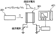
本発明においては、空隙内に上記の正孔輸送材料が注入される。空隙は電荷輸送層を挟む各種の層や電極又は基材等で構成することができる。空隙1は、例えば図1に示すように、一対の基板2,2を所定の間隔dを隔てて対向配置させることにより構成することができる。この基板2,2は、図1に示すように、ガラス基板2a上にITO(インジウム錫オキサイド)2bが形成されているものであってもよいし、ITO上にさらに電子注入層が形成されたものでもよいし、さらにその電子注入層上に有機EL素子を構成する発光層が形成されているものであってよく、特に限定されない。
In the present invention, the hole transport material is injected into the gap. The voids can be composed of various layers, electrodes, or substrates that sandwich the charge transport layer. For example, as shown in FIG. 1, the
酸素遮断手段は、正孔輸送材料を空隙内に注入する際に、その正孔輸送材料中に酸素が混入しないようにする手段であれば各種の手段を適用することができる。具体例としては、毛細管現象を利用して正孔輸送材料を空隙内に注入する方法や、不活性雰囲気中での圧着方法を利用して正孔輸送材料を空隙内に注入する方法等を例示できる。なお、不活性雰囲気中での圧着方法とは、不活性雰囲気中で素子形成領域に溶融させた正孔輸送材料を滴下した後、その正孔輸送材料を挟むように封止基板を設けて酸素を遮断する方法であり、この方法により空隙内に正孔輸送材料を注入できる。本発明においては、こうした酸素遮断手段により、正孔輸送材料に混合される可能性のある大気中の酸素を遮断することができる、また、酸素を少なくした不活性ガス中であっても、その中に僅かに含まれる酸素を遮断することができる。なお、注入時のほか、正孔輸送材料の保存時や注入工程の準備段階であっても酸素を遮断することが望ましいのは、言うまでもない。 As the oxygen blocking means, various means can be applied as long as oxygen is not mixed into the hole transport material when the hole transport material is injected into the gap. Specific examples include a method of injecting a hole transport material into the gap using a capillary phenomenon, a method of injecting a hole transport material into the gap using a pressure bonding method in an inert atmosphere, and the like. it can. Note that the pressure bonding method in an inert atmosphere is a method in which a hole transport material melted in an element formation region in an inert atmosphere is dropped, and then a sealing substrate is provided so as to sandwich the hole transport material. The hole transport material can be injected into the voids by this method. In the present invention, such oxygen blocking means can block oxygen in the atmosphere that may be mixed with the hole transport material, and even in an inert gas with reduced oxygen, Oxygen contained in the inside can be cut off. Needless to say, it is desirable to block oxygen not only at the time of injection but also at the time of storage of the hole transport material or at the preparation stage of the injection process.
こうした方法で正孔輸送材料が注入されることによって、両極性を有する電荷輸送層が形成される。その結果、本来的に両極性の電荷輸送能を有する正孔輸送材料でありながらその材料中に混入した酸素で電子がトラップされてあたかも電子輸送能を発現しないと認知されていた材料であっても、本発明の方法により、両極性を有する電荷輸送層を形成することができる。 By injecting the hole transport material by such a method, a charge transport layer having both polarities is formed. As a result, although it is a hole transport material that originally has a bipolar charge transport capability, it was recognized that electrons were trapped by oxygen mixed in the material as if it did not exhibit the electron transport capability. In addition, the charge transport layer having both polarities can be formed by the method of the present invention.
(有機半導体構造物及びその製造方法)
本発明の有機半導体構造物は、上記の電荷輸送層の形成方法により形成される両極性の電荷輸送層を有するものである。
(Organic semiconductor structure and manufacturing method thereof)
The organic semiconductor structure of the present invention has an ambipolar charge transport layer formed by the method for forming a charge transport layer described above.
その電荷輸送層が液晶性を有するものである場合には、有機半導体構造物にポリイミド膜のような配向層を設けてその電荷輸送層に配向性を持たせることもできる。また、例えば、有機EL素子について例示すれば、さらに、正孔輸送層、電子輸送層、正孔注入層、電子注入層、発光層、等の各種の層を備えた有機半導体構造物とすることができる。また、例えば、有機TFTについて例示すれば、ドレイン電極、ソース電極、ゲート電極、チャネル層、拡散層、ゲート絶縁膜等の各層を備えた有機半導体構造物とすることができる。 In the case where the charge transport layer has liquid crystallinity, an orientation layer such as a polyimide film can be provided on the organic semiconductor structure so that the charge transport layer has orientation. In addition, for example, for an organic EL element, an organic semiconductor structure provided with various layers such as a hole transport layer, an electron transport layer, a hole injection layer, an electron injection layer, a light emitting layer, etc. Can do. In addition, for example, for an organic TFT, an organic semiconductor structure including layers such as a drain electrode, a source electrode, a gate electrode, a channel layer, a diffusion layer, and a gate insulating film can be provided.
なお、上述した基板は、絶縁性の材料であれば広い範囲の材料から選択することができる。例えば、ガラス、アルミナ焼結体などの無機材料、ポリイミド膜、ポリエステル膜、ポリエチレン膜、ポリフェニレンスルフィド膜、ポリパラキシレン膜等の各種の絶縁性材料を挙げることができる。電極についても、ITO電極等の透明電極の他、ポリアニリン、ポリチオフェン等の有機材料からなる電極、導電性インキを塗布して形成した電極、金属電極であってもよい。 Note that the substrate described above can be selected from a wide range of materials as long as they are insulating materials. Examples thereof include various insulating materials such as glass, an inorganic material such as an alumina sintered body, a polyimide film, a polyester film, a polyethylene film, a polyphenylene sulfide film, and a polyparaxylene film. The electrode may be a transparent electrode such as an ITO electrode, an electrode made of an organic material such as polyaniline or polythiophene, an electrode formed by applying conductive ink, or a metal electrode.
以上、本発明の有機半導体構造物によれば、本来的に両極性の電荷輸送能を有する正孔輸送材料でありながらその材料中に混入した酸素で電子がトラップされてあたかも電子輸送能を発現しないと認知されていた材料を用いて、新規な有機半導体構造物を構成することができる。こうして得られた有機半導体構造物は、特にフレキシブルディスプレイ装置等に利用可能な薄膜トランジスタ(有機TFTともいう。)、有機EL素子、太陽電池等、電荷輸送能を有する材料を用いた各種の有機デバイスについて、その適用の幅を一層広げることに寄与することができる。 As described above, according to the organic semiconductor structure of the present invention, although it is a hole transport material that inherently has a bipolar charge transport ability, electrons are trapped by oxygen mixed in the material, as if the electron transport ability is exhibited. A novel organic semiconductor structure can be constructed using materials that have been recognized as not. The organic semiconductor structure thus obtained can be used for various organic devices using materials having charge transporting ability, such as thin film transistors (also referred to as organic TFTs), organic EL elements, solar cells and the like that can be used particularly for flexible display devices. This can contribute to further widening the range of application.
以下に、本発明についてさらに詳しく説明する。 Hereinafter, the present invention will be described in more detail.
典型的なアモルファス材料であるTPD(N',N'-bis(3-methylphenyl)-(1,1'-biphenyl)-4,4'-diamine、東京化成工業株式会社)を準備した。このTPDは、1984年に初めて米XEROXのPaiらによって複写機の感光体材料(分子分散ポリマー)として研究されて以来、数多くの研究がされている。また、1987年にC.W.Tangらによって、有機EL素子の正孔輸送材料として蒸着によるTPD薄膜が用いられ、それ以降専ら正孔輸送材料として認知され、扱われてきた。 A typical amorphous material, TPD (N ′, N′-bis (3-methylphenyl)-(1,1′-biphenyl) -4,4′-diamine, Tokyo Chemical Industry Co., Ltd.) was prepared. This TPD has been studied since 1984 for the first time as a photoconductor material (molecular dispersion polymer) for copying machines by Pai et al. Of US XEROX. In 1987, C.I. W. Tang et al. Used a vapor-deposited TPD thin film as a hole transport material for an organic EL device, and thereafter has been recognized and handled exclusively as a hole transport material.
先ず、酸素を遮断するように注意深く取り扱ったTPDを蒸留ヘキサンに溶解させ、活性炭処理をした。その後、ミリポアフィルターを用いて、活性炭や溶媒に不要な不純物を除去した後、再結晶にて精製を行った。溶媒を十分に乾燥させた後、等方相温度まで加熱し、図1に示す態様のサンドイッチセルに対して注入を行った。 First, TPD treated carefully so as to block oxygen was dissolved in distilled hexane and treated with activated carbon. Thereafter, unnecessary impurities in the activated carbon and the solvent were removed using a Millipore filter, and purification was performed by recrystallization. After the solvent was sufficiently dried, it was heated to an isotropic phase temperature and injected into the sandwich cell of the embodiment shown in FIG.
具体的には、先ず、スパチュラに粉末試料を取り、ホットステージを用いて、試料を融点程度よりやや上の温度まで加熱する。溶融した試料を、図1に示すような、あらかじめ内側にITO電極が蒸着されている間隔15μmの空隙を有するサンドイッチセルに対し、毛細管現象を利用して注入した。均一に注入された後は、余分な試料を拭き取り、ホットステージからセルを取り除き、室温において冷却を行った。 Specifically, first, a powder sample is taken in a spatula, and the sample is heated to a temperature slightly above the melting point using a hot stage. The molten sample was injected into a sandwich cell having a gap of 15 μm spacing, on which ITO electrodes were previously deposited, as shown in FIG. After the uniform injection, the excess sample was wiped off, the cell was removed from the hot stage, and cooling was performed at room temperature.
TPDの融点の文献値は169.6℃で、再結晶後のサンプルでDSC測定により求めた融点は170.1℃であった。両者はよい一致を示しており、過剰な不純物は含んでいないと考えられた。DSC測定の条件は、30〜200℃(5℃/min)及び200℃〜−50℃(5℃/min)で行った。 The literature value of the melting point of TPD was 169.6 ° C., and the melting point determined by DSC measurement of the sample after recrystallization was 170.1 ° C. Both were in good agreement and were considered not to contain excess impurities. The DSC measurement conditions were 30 to 200 ° C. (5 ° C./min) and 200 ° C. to −50 ° C. (5 ° C./min).
セルに注入した材料は、室温では偏光顕微鏡観察により均質なアモルファス状態であることが確認された。一方、徐々に加熱をしていくと、Tm付近で、ガラスがほどけて結晶化していく様子が、セルによる偏光顕微鏡観察からも確認でき、DSCの結果と一致していた。また、ガラス基板に対しTPDを溶融させキャストにより作製した厚さ15μmの薄膜について、XRDの測定を行なったところ、低分子ガラス材料として特徴的な微小領域における秩序構造を反映したブロードなハーローを確認することができた。また、結晶化などに由来するピークは観察できておらず、TPDの薄膜が均一なアモルファス状態であることを確認した。 The material injected into the cell was confirmed to be in a homogeneous amorphous state at room temperature by observation with a polarizing microscope. On the other hand, when gradually heated, the manner in which the glass was unwound and crystallized in the vicinity of Tm could be confirmed from the polarization microscope observation using the cell, which was consistent with the DSC result. In addition, XRD measurement was performed on a thin film with a thickness of 15 μm made by casting TPD on a glass substrate, and a broad harrow reflecting the ordered structure in a microscopic region characteristic of a low molecular glass material was confirmed. We were able to. Moreover, the peak derived from crystallization etc. was not able to be observed, but it confirmed that the thin film of TPD was a uniform amorphous state.
セルに注入した素子を用い、ホットプレート上で図2に示す装置を用いた定常光電流測定(TOF法)によりバイアス50Vで電荷移動度を測定した。予めUV測定により、本材料が337nm付近に強い吸収があることを確認し、光吸収に伴ったキャリア生成とその輸送を確認するために定常光照射により、光電流を確認した。光源は、Xeランプ(500W)で、赤外と紫外短波長領域はフィルターをかけている(300〜400nm)。光強度は2.4mW/cm2とした。 Using the device injected into the cell, charge mobility was measured at a bias of 50 V by means of steady photocurrent measurement (TOF method) using the apparatus shown in FIG. 2 on a hot plate. It was confirmed in advance by UV measurement that the material had strong absorption in the vicinity of 337 nm, and photocurrent was confirmed by steady light irradiation in order to confirm carrier generation and transport accompanying light absorption. The light source is a Xe lamp (500 W), and the infrared and ultraviolet short wavelength regions are filtered (300 to 400 nm). The light intensity was 2.4 mW / cm 2 .
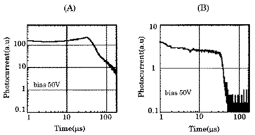
TOF法により得られた過渡光電流波形を観測したところ、図3(A)に示すように正孔輸送能に関しては従来からの正孔輸送特性が得られた。さらに、図3(B)に示すように、今までには報告例のない電子の輸送が観測できた。電子の輸送に関しては、光の浸透深さに対して十分大きな厚さを持つ試料(25μm)を用いても明確に見ることができた。なお、このデータについては、対向電極側において光励起された分子による正孔輸送ではなく、電子の輸送による信号を観測していると言える。 When the transient photocurrent waveform obtained by the TOF method was observed, as shown in FIG. 3A, conventional hole transport characteristics were obtained with respect to the hole transport ability. Furthermore, as shown in FIG. 3B, electron transport that has never been reported has been observed. Regarding electron transport, it was possible to clearly see even when a sample (25 μm) having a sufficiently large thickness with respect to the penetration depth of light was used. In addition, about this data, it can be said that the signal by electron transport is observed rather than the hole transport by the molecule | numerator photoexcited by the counter electrode side.
1 空隙
2 基板
2a ガラス基板
2b ITO電極
d 空隙の間隔
201 N2パルスレーザー
301 試料
401 デジタルオシロスコープ
1
Claims (5)
Priority Applications (1)
| Application Number | Priority Date | Filing Date | Title |
|---|---|---|---|
| JP2004108527A JP2005294587A (en) | 2004-03-31 | 2004-03-31 | Method for forming charge transport layer, organic semiconductor structure and method for producing the same |
Applications Claiming Priority (1)
| Application Number | Priority Date | Filing Date | Title |
|---|---|---|---|
| JP2004108527A JP2005294587A (en) | 2004-03-31 | 2004-03-31 | Method for forming charge transport layer, organic semiconductor structure and method for producing the same |
Publications (1)
| Publication Number | Publication Date |
|---|---|
| JP2005294587A true JP2005294587A (en) | 2005-10-20 |
Family
ID=35327170
Family Applications (1)
| Application Number | Title | Priority Date | Filing Date |
|---|---|---|---|
| JP2004108527A Withdrawn JP2005294587A (en) | 2004-03-31 | 2004-03-31 | Method for forming charge transport layer, organic semiconductor structure and method for producing the same |
Country Status (1)
| Country | Link |
|---|---|
| JP (1) | JP2005294587A (en) |
Cited By (1)
| Publication number | Priority date | Publication date | Assignee | Title |
|---|---|---|---|---|
| JP2015099155A (en) * | 2009-09-16 | 2015-05-28 | 独立行政法人科学技術振興機構 | Liquid organic semiconductor materials |
-
2004
- 2004-03-31 JP JP2004108527A patent/JP2005294587A/en not_active Withdrawn
Cited By (1)
| Publication number | Priority date | Publication date | Assignee | Title |
|---|---|---|---|---|
| JP2015099155A (en) * | 2009-09-16 | 2015-05-28 | 独立行政法人科学技術振興機構 | Liquid organic semiconductor materials |
Similar Documents
| Publication | Publication Date | Title |
|---|---|---|
| Wang et al. | Investigation of electrode electrochemical reactions in CH3NH3PbBr3 perovskite single‐crystal field‐effect transistors | |
| Jang et al. | Highly crystalline soluble acene crystal arrays for organic transistors: mechanism of crystal growth during dip‐coating | |
| Minari et al. | Controlled Self‐Assembly of Organic Semiconductors for Solution‐Based Fabrication of Organic Field‐Effect Transistors | |
| Chen et al. | Vacuum‐assisted preparation of high‐quality quasi‐2D perovskite thin films for large‐area light‐emitting diodes | |
| WO2007026778A1 (en) | Transistor, organic semiconductor device, and method for manufacture of the transistor or device | |
| CN103972388B (en) | The method for preparing the controllable highly oriented organic small molecular semiconductor single grain pattern of size | |
| Kim et al. | High-Performance Green Light-Emitting Diodes Based on MAPbBr3–Polymer Composite Films Prepared by Gas-Assisted Crystallization | |
| Lin et al. | Organic liquid crystals in optoelectronic device applications: Field‐effect transistors, nonvolatile memory, and photovoltaics | |
| Ji et al. | Perovskite Light‐Emitting Diode Display Based on MoS2 Backplane Thin‐Film Transistors | |
| WO2013065582A1 (en) | Method for producing organic semiconductor element, organic semiconductor element, method for growing organic single crystal thin film, organic single crystal thin film, electronic device and group of organic single crystal thin films | |
| Peng et al. | A Transfer Method for High‐Mobility, Bias‐Stable, and Flexible Organic Field‐Effect Transistors | |
| Yun et al. | Effect of laser-induced direct micropatterning on polymer optoelectronic devices | |
| TW200908408A (en) | Tetracarboxylic diimide semiconductor for thin film transistors | |
| Xia et al. | Solvent‐Free Coating of Organic Semiconductor Membranes with Centimetric Crystalline Domains | |
| EP3188219A1 (en) | Fabrication method of semiconductor film, semiconductor film, and field effect transistor | |
| JP4587276B2 (en) | Method for producing film made of liquid crystal polymer | |
| Wang et al. | Pre‐Nucleation Strategy for Room‐Temperature Growth of Perovskite Single Crystals toward Efficient Perovskite Light‐Emitting Diodes | |
| Katz et al. | Mesophase transitions, surface functionalization, and growth mechanism of semiconducting 6PTTP6 films from solution | |
| WO2013065276A1 (en) | Organic single crystal film, organic single crystal film array, and semiconductor device including an organic single crystal film | |
| US7709830B2 (en) | Organic semiconductor structure, manufacturing method of the same, and organic semiconductor device | |
| WO2014136436A1 (en) | Organic thin film transistor and method for manufacturing same | |
| JP2005294587A (en) | Method for forming charge transport layer, organic semiconductor structure and method for producing the same | |
| TW200537569A (en) | Thin film of condensed polycyclic aromatic compound, and method for preparing thin film of condensed polycyclic aromatic compound | |
| WO2014136942A1 (en) | Method for forming organic thin film | |
| JP4673135B2 (en) | Method for forming organic semiconductor layer |
Legal Events
| Date | Code | Title | Description |
|---|---|---|---|
| A300 | Application deemed to be withdrawn because no request for examination was validly filed |
Free format text: JAPANESE INTERMEDIATE CODE: A300 Effective date: 20070605 |