JP2005294576A - Digital amplifier board - Google Patents
Digital amplifier board Download PDFInfo
- Publication number
- JP2005294576A JP2005294576A JP2004108299A JP2004108299A JP2005294576A JP 2005294576 A JP2005294576 A JP 2005294576A JP 2004108299 A JP2004108299 A JP 2004108299A JP 2004108299 A JP2004108299 A JP 2004108299A JP 2005294576 A JP2005294576 A JP 2005294576A
- Authority
- JP
- Japan
- Prior art keywords
- digital amplifier
- heat
- amplifier board
- shield case
- electronic components
- Prior art date
- Legal status (The legal status is an assumption and is not a legal conclusion. Google has not performed a legal analysis and makes no representation as to the accuracy of the status listed.)
- Pending
Links
Images

Landscapes
- Shielding Devices Or Components To Electric Or Magnetic Fields (AREA)
- Cooling Or The Like Of Electrical Apparatus (AREA)
- Amplifiers (AREA)
Abstract
【課題】 本発明は、デジタルアンプ基板に実装された電子部品から発生する熱を効率よく放熱することができ、熱による電子部品の故障を防止することができるデジタルアンプ基板を提供することを課題とする。
【解決手段】 放熱板11は、黄銅等、熱伝導性の高く、且つ導電性を有する金属材料で構成され、デジタルアンプ基板10に実装された電子部品の内、発熱量の大きい発熱部品に接触させて配置されている。シールドケース12は、鉄板等の導電性を有する金属材料で構成され、放熱板11をその一部として閉空間を形成し、当該閉空間内にデジタルアンプ基板10を包み込む。また、シールドケース12には、包み込んだデジタルアンプ基板10への空気の対流を促進させるための放熱穴13が複数形成されている。
【選択図】 図1PROBLEM TO BE SOLVED: To provide a digital amplifier board capable of efficiently dissipating heat generated from electronic components mounted on a digital amplifier board and preventing failure of the electronic parts due to heat. And
A heat dissipation plate is made of a metal material having high heat conductivity and conductivity, such as brass, and contacts a heat generating component having a large heat generation amount among electronic components mounted on a digital amplifier substrate. Are arranged. The shield case 12 is made of a conductive metal material such as an iron plate, forms a closed space with the heat sink 11 as a part thereof, and encloses the digital amplifier board 10 in the closed space. The shield case 12 is formed with a plurality of heat radiation holes 13 for promoting air convection to the enclosed digital amplifier substrate 10.
[Selection] Figure 1
Description
本発明は、スイッチング増幅、すなわちスイッチング素子のON/OFF処理によってアナログ信号の増幅を行うデジタルアンプ回路が実装されたデジタルアンプ基板に関し、特にデジタルアンプ回路から発生する電磁波の輻射対策を施したデジタルアンプ基板に関する。 The present invention relates to a digital amplifier substrate on which a digital amplifier circuit that performs analog amplification of switching signals, that is, an analog signal by switching ON / OFF processing of the switching element, and more particularly, a digital amplifier that takes measures against radiation of electromagnetic waves generated from the digital amplifier circuit. Regarding the substrate.
近年、入力されたアナログ信号をパルス幅変調(PWM)やパルス密度変調(PDM)等で変調処理してデジタル信号に変換し、変換したデジタル信号をスイッチング素子でスイッチング増幅を行い、ローパスフィルタによってアナログ信号に戻す、デジタルアンプ回路を増幅器として採用するAV機器が増加している。 In recent years, input analog signals are modulated by pulse width modulation (PWM), pulse density modulation (PDM), etc., and converted to digital signals. The converted digital signals are switched and amplified by a switching element, and analog by a low-pass filter. There is an increasing number of AV devices that use digital amplifier circuits as amplifiers to return signals.
デジタルアンプ回路は、スイッチング素子のON/OFF処理によってアナログ信号の増幅を行うことができるため、理論的には100%の電力効率が得られ、消費電力や発熱量が低いと共に、高出力が得られるという利点があると共に、発熱量が低いという利点があるため、省スペース化を実現でき、AV装置の薄型化が促進されている。 Since the digital amplifier circuit can amplify analog signals by ON / OFF processing of switching elements, theoretically 100% power efficiency can be obtained, low power consumption and low heat generation, and high output can be obtained. In addition, there is an advantage that the calorific value is low, so that space saving can be realized, and the thinning of the AV apparatus is promoted.
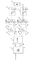
図3は、デジタルアンプ回路の構成を示す図である。
デジタルアンプ回路は、図3を参照すると、PDM処理部1と、ロジック部2と、ゲートドライバ3と、スイッチング回路部4と、ローパスフィルタ(LPF)5と、ゲートドライバ7と、スイッチング回路部8と、ローパスフィルタ(LPF)9とにより構成され、スピーカ等の負荷6がスイッチング回路部4とスイッチング回路部8とによってバランス駆動される。
FIG. 3 is a diagram illustrating a configuration of the digital amplifier circuit.
Referring to FIG. 3, the digital amplifier circuit includes a
PDM処理部1は、入力されたアナログ信号を、HIGH/LOWの2値に高速に変化する信号で表現するパルス密度変調信号S1に変換してロジック部2に出力すると共に、パルス密度変調信号S1を位相反転したパルス密度変調信号S2をロジック部2に出力する。ロジック部2は、PDM処理部1からのパルス密度変調信号S1、S2をゲートドライバ3、7に振り分け、ゲートドライバ3、7は、ロジック部2からのパルス密度変調信号S1、S2をスイッチング回路部4およびスイッチング回路部8を駆動できる程度に増幅する。
The
スイッチング回路部4は、NチャンネルのMOSFET素子41およびNチャンネルのMOSFET素子42を有し、MOSFET素子41のソースとMOSFET素子42のドレインの間が直列に接続され、MOSFET素子41のドレイン側が出力用電源に接続され、MOSFET素子42のソース側が接地されている。同様に、スイッチング回路部8は、NチャンネルのMOSFET素子81およびNチャンネルのMOSFET素子82を有し、MOSFET素子81のソースとMOSFET素子82のドレインの間が直列に接続され、MOSFET素子81のドレイン側が出力用電源に接続され、MOSFET素子82のソース側が接地されている。
The switching circuit unit 4 includes an N-channel MOSFET element 41 and an N-
LPF5は、チョークコイル51とコンデンサ52とを有し、チョークコイル51の一方側が、MOSFET素子41のソースとMOSFET素子42のドレインとの間の直列接続点に接続されている。また、チョークコイル51の他方側およびコンデンサ52の一方側の夫々が出力側に接続され、コンデンサ52の他方側が接地されている。同様に、LPF9は、チョークコイル91とコンデンサ92とを有し、チョークコイル91の一方側が、MOSFET素子81のソースとMOSFET素子82のドレインとの間の直列接続点に接続されている。また、チョークコイル91の他方側およびコンデンサ92の一方側の夫々が出力側に接続され、コンデンサ92の他方側が接地されている。
The
このようなデジタルアンプ基板においては、スイッチング回路部4およびスイッチング回路部8で出力用電源とグランド間で高速にスイッチングしているため、各MOSFET素子の消費電流の微分成分が出力用電源の立ち上がりエッジおよび立ち下がりエッジに重畳され、各MOSFET素子の消費電流の微分成分が本来予定されていない輻射電磁波(以下、不要輻射と称す)として放射されてしまう。そこで、スイッチング回路部4およびスイッチング回路部8等の輻射発生源が存在するデジタルアンプ基板をシールドする必要があるが、従来は、デジタルアンプ基板のグランド用銅箔と、シールド筐体とにより、輻射発生源を閉空間で取り囲み、不要輻射をシールドするのが一般的である(例えば、特許文献1参照)。 In such a digital amplifier substrate, the switching circuit unit 4 and the switching circuit unit 8 perform high-speed switching between the output power supply and the ground, so that the differential component of the current consumption of each MOSFET element is the rising edge of the output power supply. In addition, the differential component of the current consumption of each MOSFET element is radiated as a radiation electromagnetic wave (hereinafter referred to as unnecessary radiation) that is not originally scheduled, superimposed on the falling edge. Therefore, it is necessary to shield the digital amplifier board on which radiation sources such as the switching circuit unit 4 and the switching circuit unit 8 exist. Conventionally, radiation is radiated by the ground copper foil of the digital amplifier board and the shield housing. Generally, the generation source is surrounded by a closed space to shield unwanted radiation (see, for example, Patent Document 1).
しかしながら、従来技術では、デジタルアンプ基板側からの輻射を確実にシールドすることができず、スイッチング増幅によって輻射された電磁波がデジタルアンプ基板側から外部に放射されてしまうと共に、デジタルアンプ基板に実装された電子部品からの発生する熱がグランド用銅箔とシールド筐体とによって形成された閉空間にこもってしまい、電子部品自体の故障の一因となってしまうという問題点があった。
本発明は斯かる問題点を鑑みてなされたものであり、その目的とするところは、デジタルアンプ基板側からの輻射を確実にシールドすることができ、スイッチング増幅による不要輻射がデジタルアンプ基板側から外部に放射されることがないと共に、デジタルアンプ基板に実装された電子部品からの発生する熱を効率よく放熱することができ、熱による電子部品の故障を防止することができるデジタルアンプ基板を提供する点にある。 The present invention has been made in view of such problems, and the object of the present invention is to reliably shield radiation from the digital amplifier board side, and unnecessary radiation due to switching amplification from the digital amplifier board side. Providing a digital amplifier board that is not radiated to the outside, can efficiently dissipate heat generated from electronic components mounted on the digital amplifier board, and can prevent failure of electronic parts due to heat There is in point to do.
本発明は上記課題を解決すべく、以下に掲げる構成とした。
本発明のデジタルアンプ基板は、スイッチング素子のON/OFF処理によってアナログ信号の増幅を行うデジタルアンプ回路が実装されたデジタルアンプ基板であって、実装された電子部品の内の発熱量が大きい発熱部品に接触させて配置された放熱板と、該放熱板をその一部として閉空間を形成するシールドケースとによって包み込まれていることを特徴とする。
In order to solve the above problems, the present invention has the following configuration.
The digital amplifier board of the present invention is a digital amplifier board on which a digital amplifier circuit that amplifies an analog signal by ON / OFF processing of a switching element is mounted, and a heat generating component that generates a large amount of heat among the mounted electronic components It is characterized by being encased by a heat radiating plate disposed in contact with the heat sink and a shield case that forms a closed space with the heat radiating plate as a part thereof.
さらに、本発明のデジタルアンプ基板は、前記シールドケースには、不要輻射の周波数帯域での波長以内の寸法の放熱穴が複数形成されていることを特徴とする。 Furthermore, the digital amplifier board of the present invention is characterized in that the shield case is formed with a plurality of heat radiation holes having dimensions within a wavelength in the frequency band of unnecessary radiation.
本発明のデジタルアンプ基板は、デジタルアンプ基板を、発熱量の大きい発熱部品に接触させて配置された放熱板と、シールドケースとによって包み込むように構成することにより、デジタルアンプ基板側からの輻射を確実にシールドすることができ、スイッチング増幅による不要輻射がデジタルアンプ基板側から外部に放射されることがないと共に、デジタルアンプ基板に実装された電子部品からの発生する熱を効率よく放熱することができ、熱による電子部品の故障を防止することができるという効果を奏する。 The digital amplifier board of the present invention is configured so that the digital amplifier board is wrapped by a heat radiating plate disposed in contact with a heat-generating component having a large calorific value and a shield case, thereby radiating radiation from the digital amplifier board side. It can be shielded reliably, and unnecessary radiation due to switching amplification is not radiated to the outside from the digital amplifier board side, and heat generated from electronic components mounted on the digital amplifier board can be efficiently radiated. It is possible to produce an effect that the failure of the electronic component due to heat can be prevented.
さらに、本発明のデジタルアンプ基板は、デジタルアンプ基板を包み込んだシールドケースに空気の対流を促進させるための放熱穴を複数形成することにより、デジタルアンプ基板に実装された電子部品からの発生する熱をより効率よく放熱することができ、熱による電子部品の故障を防止することができる Furthermore, the digital amplifier board of the present invention is formed by forming a plurality of heat radiating holes for promoting air convection in a shield case enclosing the digital amplifier board, thereby generating heat generated from electronic components mounted on the digital amplifier board. Heat can be dissipated more efficiently, and failure of electronic components due to heat can be prevented.
以下、本発明の実施の形態を図面に基づいて詳細に説明する。 Hereinafter, embodiments of the present invention will be described in detail with reference to the drawings.
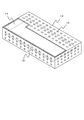
図1は、本発明に係るデジタルアンプ基板の実施の形態の構成を示す概略斜視図あり、図2は、図1に示すデジタルアンプ基板の構成を示す図であり、(a)は、上面図であり、(b)は、(a)に示すX−Y断面図である。
である。
FIG. 1 is a schematic perspective view showing a configuration of an embodiment of a digital amplifier board according to the present invention, FIG. 2 is a diagram showing a configuration of the digital amplifier board shown in FIG. 1, and (a) is a top view. (B) is an XY cross-sectional view shown in (a).
It is.
本実施の形態は、PDM処理部1と、ロジック部2と、ゲートドライバ3と、スイッチング回路部4と、ローパスフィルタ(LPF)5と、ゲートドライバ7と、スイッチング回路部8と、ローパスフィルタ(LPF)9とにより構成され、スピーカ等の負荷6を駆動するデジタルアンプ回路が実装されたデジタルアンプ基板10を、図1に示すように、放熱板11と、シールドケース12とによって包み込む構成となっている。
In this embodiment, a
放熱板11は、黄銅等、熱伝導性の高く、且つ導電性を有する金属材料で構成され、図2を参照すると、デジタルアンプ基板10に実装された電子部品の内、発熱量の大きい発熱部品14に接触させて配置されている。従って、発熱部品14が発生する熱は、放熱板11に伝導され、放熱板11に伝導された熱は、放熱板11の表面と外気との温度差によって表面から放熱される。
The
シールドケース12は、鉄板等の導電性を有する金属材料で構成され、放熱板11をその一部として閉空間を形成し、当該閉空間内にデジタルアンプ基板10を包み込んで、デジタルアンプ基板10からの不要輻射をシールドする。
The
また、シールドケース12には、包み込んだデジタルアンプ基板10への空気の対流を促進させるための放熱穴13が複数形成されており、デジタルアンプ基板10に実装された電子部品が発生する熱の放熱効率を高めることができるように構成されている。なお、放熱穴13は、不要輻射が洩れない程度の大きさであり、具体的には、シールドを行う不要輻射の周波数帯域での波長以内の寸法にする。放熱穴13が円形である場合には、その直径を不要輻射の周波数帯域での波長以内にすれば良い。
The
なお、放熱板11およびシールドケース12の取り付け構造については、特に図示していないが、例えば、発熱部品14と放熱板11とを接触した状態でビス留め等によって固定すると共に、デジタルアンプ基板10とシールドケース12とをビス留め等によって固定するようにすれば良く、さらに、放熱板11とシールドケース12とをビス留め等によって固定するようにしても良い。
The mounting structure of the
以上説明したように、本実施の形態によれば、デジタルアンプ基板10を、発熱量の大きい発熱部品14に接触させて配置された放熱板11と、シールドケース12とによって包み込まように構成することにより、デジタルアンプ基板側からの輻射を確実にシールドすることができ、スイッチング増幅による不要輻射がデジタルアンプ基板側から外部に放射されることがないと共に、デジタルアンプ基板10に実装された電子部品からの発生する熱を効率よく放熱することができ、熱による電子部品の故障を防止することができるという効果を奏する。
As described above, according to the present embodiment, the
さらに、本実施の形態によれば、デジタルアンプ基板10を包み込んだシールドケース12に空気の対流を促進させるための放熱穴13を複数形成することにより、デジタルアンプ基板10に実装された電子部品からの発生する熱をより効率よく放熱することができ、熱による電子部品の故障を防止することができる。
Furthermore, according to the present embodiment, by forming a plurality of
なお、本発明が上記各実施の形態に限定されず、本発明の技術思想の範囲内において、各実施の形態は適宜変更され得ることは明らかである。また、上記構成部材の数、位置、形状等は上記実施の形態に限定されず、本発明を実施する上で好適な数、位置、形状等にすることができる。なお、各図において、同一構成要素には同一符号を付している。 Note that the present invention is not limited to the above-described embodiments, and it is obvious that the embodiments can be appropriately changed within the scope of the technical idea of the present invention. In addition, the number, position, shape, and the like of the constituent members are not limited to the above-described embodiment, and can be set to a suitable number, position, shape, and the like in practicing the present invention. In each figure, the same numerals are given to the same component.
1 PDM処理部
2 ロジック部
3 ゲートドライバ
4 スイッチング回路部
5 ローパスフィルタ(LPF)
6 負荷
7 ゲートドライバ
8 スイッチング回路部
9 ローパスフィルタ(LPF)
10 デジタルアンプ基板
11 放熱板
12 シールドケース
13 放熱穴
14 発熱部品
41、42 MOSFET素子
51 チョークコイル
52 コンデンサ
81、82 MOSFET素子
91 チョークコイル
92 コンデンサ
DESCRIPTION OF
6 Load 7 Gate driver 8 Switching circuit 9 Low pass filter (LPF)
DESCRIPTION OF
Claims (2)
実装された電子部品の内の発熱量が大きい発熱部品に接触させて配置された放熱板と、
該放熱板をその一部として閉空間を形成するシールドケースとによって包み込まれていることを特徴とするデジタルアンプ基板。 A digital amplifier board on which a digital amplifier circuit that amplifies an analog signal by ON / OFF processing of a switching element is mounted,
A heat sink arranged in contact with a heat generating component that generates a large amount of heat among the mounted electronic components;
A digital amplifier substrate which is wrapped by a shield case which forms a closed space with the heat radiating plate as a part thereof.
2. The digital amplifier board according to claim 1, wherein the shield case is formed with a plurality of heat radiation holes having dimensions within a wavelength in a frequency band of unnecessary radiation.
Priority Applications (1)
| Application Number | Priority Date | Filing Date | Title |
|---|---|---|---|
| JP2004108299A JP2005294576A (en) | 2004-03-31 | 2004-03-31 | Digital amplifier board |
Applications Claiming Priority (1)
| Application Number | Priority Date | Filing Date | Title |
|---|---|---|---|
| JP2004108299A JP2005294576A (en) | 2004-03-31 | 2004-03-31 | Digital amplifier board |
Publications (1)
| Publication Number | Publication Date |
|---|---|
| JP2005294576A true JP2005294576A (en) | 2005-10-20 |
Family
ID=35327163
Family Applications (1)
| Application Number | Title | Priority Date | Filing Date |
|---|---|---|---|
| JP2004108299A Pending JP2005294576A (en) | 2004-03-31 | 2004-03-31 | Digital amplifier board |
Country Status (1)
| Country | Link |
|---|---|
| JP (1) | JP2005294576A (en) |
Cited By (3)
| Publication number | Priority date | Publication date | Assignee | Title |
|---|---|---|---|---|
| JP2007259262A (en) * | 2006-03-24 | 2007-10-04 | Sharp Corp | Audio equipment |
| CN105932985A (en) * | 2016-04-10 | 2016-09-07 | 安徽众尚微波科技有限公司 | Microwave intermediate-frequency signal generator |
| WO2021153340A1 (en) * | 2020-01-27 | 2021-08-05 | ローム株式会社 | Class-d amplifier module, audio system, and automobile |
-
2004
- 2004-03-31 JP JP2004108299A patent/JP2005294576A/en active Pending
Cited By (5)
| Publication number | Priority date | Publication date | Assignee | Title |
|---|---|---|---|---|
| JP2007259262A (en) * | 2006-03-24 | 2007-10-04 | Sharp Corp | Audio equipment |
| CN105932985A (en) * | 2016-04-10 | 2016-09-07 | 安徽众尚微波科技有限公司 | Microwave intermediate-frequency signal generator |
| CN105932985B (en) * | 2016-04-10 | 2018-08-31 | 安徽众尚微波科技有限公司 | A kind of microwave signal generator of intermediate frequency |
| WO2021153340A1 (en) * | 2020-01-27 | 2021-08-05 | ローム株式会社 | Class-d amplifier module, audio system, and automobile |
| JP7588100B2 (en) | 2020-01-27 | 2024-11-21 | ローム株式会社 | Audio systems, automobiles |
Similar Documents
| Publication | Publication Date | Title |
|---|---|---|
| WO2004032249A3 (en) | Optoelectronic component and a module based thereon | |
| US20040164405A1 (en) | Heatsink arrangement for semiconductor device | |
| JP4978265B2 (en) | High frequency module | |
| JPWO2009037995A1 (en) | High power amplifier, wireless transmitter, wireless transceiver, and high power amplifier mounting method | |
| JP5577694B2 (en) | Built-in module | |
| JP2005026263A (en) | Hybrid integrated circuit | |
| JPH098482A (en) | Heat dissipating method of switching element | |
| JP2005294576A (en) | Digital amplifier board | |
| JP2005294574A (en) | Digital amplifier device | |
| JP4654764B2 (en) | Mounting structure of high-frequency circuit device | |
| JP2010278113A (en) | Communication module | |
| JP2007259262A (en) | Audio equipment | |
| JP2007259250A (en) | Audio equipment | |
| JP4770518B2 (en) | High power amplifier | |
| JP2008125283A (en) | Power converter | |
| JP2001068879A (en) | Control equipment | |
| JP2002158317A (en) | Low noise heat dissipation IC package and circuit board | |
| JP2014170834A (en) | Heat radiation structure of power semiconductor and audio device using the same | |
| KR101940295B1 (en) | Board structure with radio frequency wave shield | |
| JP7226087B2 (en) | Electrical characteristic evaluation jig | |
| WO2021186797A1 (en) | Circuit board module | |
| JP4072338B2 (en) | Wireless unit | |
| JPH05167204A (en) | Printed board | |
| JP2025151477A (en) | electronic equipment | |
| JP2012079834A (en) | Heat radiation structure of heating component |