JP2005294544A - Semiconductor laser device - Google Patents
Semiconductor laser device Download PDFInfo
- Publication number
- JP2005294544A JP2005294544A JP2004107783A JP2004107783A JP2005294544A JP 2005294544 A JP2005294544 A JP 2005294544A JP 2004107783 A JP2004107783 A JP 2004107783A JP 2004107783 A JP2004107783 A JP 2004107783A JP 2005294544 A JP2005294544 A JP 2005294544A
- Authority
- JP
- Japan
- Prior art keywords
- region
- length
- semiconductor laser
- laser device
- layer
- Prior art date
- Legal status (The legal status is an assumption and is not a legal conclusion. Google has not performed a legal analysis and makes no representation as to the accuracy of the status listed.)
- Granted
Links
Images


Classifications
-
- H—ELECTRICITY
- H01—ELECTRIC ELEMENTS
- H01S—DEVICES USING THE PROCESS OF LIGHT AMPLIFICATION BY STIMULATED EMISSION OF RADIATION [LASER] TO AMPLIFY OR GENERATE LIGHT; DEVICES USING STIMULATED EMISSION OF ELECTROMAGNETIC RADIATION IN WAVE RANGES OTHER THAN OPTICAL
- H01S5/00—Semiconductor lasers
- H01S5/20—Structure or shape of the semiconductor body to guide the optical wave ; Confining structures perpendicular to the optical axis, e.g. index or gain guiding, stripe geometry, broad area lasers, gain tailoring, transverse or lateral reflectors, special cladding structures, MQW barrier reflection layers
- H01S5/22—Structure or shape of the semiconductor body to guide the optical wave ; Confining structures perpendicular to the optical axis, e.g. index or gain guiding, stripe geometry, broad area lasers, gain tailoring, transverse or lateral reflectors, special cladding structures, MQW barrier reflection layers having a ridge or stripe structure
- H01S5/223—Buried stripe structure
- H01S5/2231—Buried stripe structure with inner confining structure only between the active layer and the upper electrode
-
- B—PERFORMING OPERATIONS; TRANSPORTING
- B82—NANOTECHNOLOGY
- B82Y—SPECIFIC USES OR APPLICATIONS OF NANOSTRUCTURES; MEASUREMENT OR ANALYSIS OF NANOSTRUCTURES; MANUFACTURE OR TREATMENT OF NANOSTRUCTURES
- B82Y20/00—Nanooptics, e.g. quantum optics or photonic crystals
-
- H—ELECTRICITY
- H01—ELECTRIC ELEMENTS
- H01S—DEVICES USING THE PROCESS OF LIGHT AMPLIFICATION BY STIMULATED EMISSION OF RADIATION [LASER] TO AMPLIFY OR GENERATE LIGHT; DEVICES USING STIMULATED EMISSION OF ELECTROMAGNETIC RADIATION IN WAVE RANGES OTHER THAN OPTICAL
- H01S2301/00—Functional characteristics
- H01S2301/18—Semiconductor lasers with special structural design for influencing the near- or far-field
-
- H—ELECTRICITY
- H01—ELECTRIC ELEMENTS
- H01S—DEVICES USING THE PROCESS OF LIGHT AMPLIFICATION BY STIMULATED EMISSION OF RADIATION [LASER] TO AMPLIFY OR GENERATE LIGHT; DEVICES USING STIMULATED EMISSION OF ELECTROMAGNETIC RADIATION IN WAVE RANGES OTHER THAN OPTICAL
- H01S5/00—Semiconductor lasers
- H01S5/10—Construction or shape of the optical resonator, e.g. extended or external cavity, coupled cavities, bent-guide, varying width, thickness or composition of the active region
- H01S5/1039—Details on the cavity length
-
- H—ELECTRICITY
- H01—ELECTRIC ELEMENTS
- H01S—DEVICES USING THE PROCESS OF LIGHT AMPLIFICATION BY STIMULATED EMISSION OF RADIATION [LASER] TO AMPLIFY OR GENERATE LIGHT; DEVICES USING STIMULATED EMISSION OF ELECTROMAGNETIC RADIATION IN WAVE RANGES OTHER THAN OPTICAL
- H01S5/00—Semiconductor lasers
- H01S5/10—Construction or shape of the optical resonator, e.g. extended or external cavity, coupled cavities, bent-guide, varying width, thickness or composition of the active region
- H01S5/16—Window-type lasers, i.e. with a region of non-absorbing material between the active region and the reflecting surface
- H01S5/162—Window-type lasers, i.e. with a region of non-absorbing material between the active region and the reflecting surface with window regions made by diffusion or disordening of the active layer
-
- H—ELECTRICITY
- H01—ELECTRIC ELEMENTS
- H01S—DEVICES USING THE PROCESS OF LIGHT AMPLIFICATION BY STIMULATED EMISSION OF RADIATION [LASER] TO AMPLIFY OR GENERATE LIGHT; DEVICES USING STIMULATED EMISSION OF ELECTROMAGNETIC RADIATION IN WAVE RANGES OTHER THAN OPTICAL
- H01S5/00—Semiconductor lasers
- H01S5/10—Construction or shape of the optical resonator, e.g. extended or external cavity, coupled cavities, bent-guide, varying width, thickness or composition of the active region
- H01S5/16—Window-type lasers, i.e. with a region of non-absorbing material between the active region and the reflecting surface
- H01S5/168—Window-type lasers, i.e. with a region of non-absorbing material between the active region and the reflecting surface with window regions comprising current blocking layers
-
- H—ELECTRICITY
- H01—ELECTRIC ELEMENTS
- H01S—DEVICES USING THE PROCESS OF LIGHT AMPLIFICATION BY STIMULATED EMISSION OF RADIATION [LASER] TO AMPLIFY OR GENERATE LIGHT; DEVICES USING STIMULATED EMISSION OF ELECTROMAGNETIC RADIATION IN WAVE RANGES OTHER THAN OPTICAL
- H01S5/00—Semiconductor lasers
- H01S5/20—Structure or shape of the semiconductor body to guide the optical wave ; Confining structures perpendicular to the optical axis, e.g. index or gain guiding, stripe geometry, broad area lasers, gain tailoring, transverse or lateral reflectors, special cladding structures, MQW barrier reflection layers
- H01S5/22—Structure or shape of the semiconductor body to guide the optical wave ; Confining structures perpendicular to the optical axis, e.g. index or gain guiding, stripe geometry, broad area lasers, gain tailoring, transverse or lateral reflectors, special cladding structures, MQW barrier reflection layers having a ridge or stripe structure
- H01S5/2205—Structure or shape of the semiconductor body to guide the optical wave ; Confining structures perpendicular to the optical axis, e.g. index or gain guiding, stripe geometry, broad area lasers, gain tailoring, transverse or lateral reflectors, special cladding structures, MQW barrier reflection layers having a ridge or stripe structure comprising special burying or current confinement layers
- H01S5/2214—Structure or shape of the semiconductor body to guide the optical wave ; Confining structures perpendicular to the optical axis, e.g. index or gain guiding, stripe geometry, broad area lasers, gain tailoring, transverse or lateral reflectors, special cladding structures, MQW barrier reflection layers having a ridge or stripe structure comprising special burying or current confinement layers based on oxides or nitrides
-
- H—ELECTRICITY
- H01—ELECTRIC ELEMENTS
- H01S—DEVICES USING THE PROCESS OF LIGHT AMPLIFICATION BY STIMULATED EMISSION OF RADIATION [LASER] TO AMPLIFY OR GENERATE LIGHT; DEVICES USING STIMULATED EMISSION OF ELECTROMAGNETIC RADIATION IN WAVE RANGES OTHER THAN OPTICAL
- H01S5/00—Semiconductor lasers
- H01S5/30—Structure or shape of the active region; Materials used for the active region
- H01S5/34—Structure or shape of the active region; Materials used for the active region comprising quantum well or superlattice structures, e.g. single quantum well [SQW] lasers, multiple quantum well [MQW] lasers or graded index separate confinement heterostructure [GRINSCH] lasers
- H01S5/343—Structure or shape of the active region; Materials used for the active region comprising quantum well or superlattice structures, e.g. single quantum well [SQW] lasers, multiple quantum well [MQW] lasers or graded index separate confinement heterostructure [GRINSCH] lasers in AIIIBV compounds, e.g. AlGaAs-laser, InP-based laser
- H01S5/34333—Structure or shape of the active region; Materials used for the active region comprising quantum well or superlattice structures, e.g. single quantum well [SQW] lasers, multiple quantum well [MQW] lasers or graded index separate confinement heterostructure [GRINSCH] lasers in AIIIBV compounds, e.g. AlGaAs-laser, InP-based laser with a well layer based on Ga(In)N or Ga(In)P, e.g. blue laser
-
- H—ELECTRICITY
- H01—ELECTRIC ELEMENTS
- H01S—DEVICES USING THE PROCESS OF LIGHT AMPLIFICATION BY STIMULATED EMISSION OF RADIATION [LASER] TO AMPLIFY OR GENERATE LIGHT; DEVICES USING STIMULATED EMISSION OF ELECTROMAGNETIC RADIATION IN WAVE RANGES OTHER THAN OPTICAL
- H01S5/00—Semiconductor lasers
- H01S5/40—Arrangement of two or more semiconductor lasers, not provided for in groups H01S5/02 - H01S5/30
- H01S5/4025—Array arrangements, e.g. constituted by discrete laser diodes or laser bar
- H01S5/4031—Edge-emitting structures
-
- H—ELECTRICITY
- H01—ELECTRIC ELEMENTS
- H01S—DEVICES USING THE PROCESS OF LIGHT AMPLIFICATION BY STIMULATED EMISSION OF RADIATION [LASER] TO AMPLIFY OR GENERATE LIGHT; DEVICES USING STIMULATED EMISSION OF ELECTROMAGNETIC RADIATION IN WAVE RANGES OTHER THAN OPTICAL
- H01S5/00—Semiconductor lasers
- H01S5/40—Arrangement of two or more semiconductor lasers, not provided for in groups H01S5/02 - H01S5/30
- H01S5/4025—Array arrangements, e.g. constituted by discrete laser diodes or laser bar
- H01S5/4087—Array arrangements, e.g. constituted by discrete laser diodes or laser bar emitting more than one wavelength
Landscapes
- Physics & Mathematics (AREA)
- Optics & Photonics (AREA)
- Nanotechnology (AREA)
- Engineering & Computer Science (AREA)
- Chemical & Material Sciences (AREA)
- General Physics & Mathematics (AREA)
- Life Sciences & Earth Sciences (AREA)
- Biophysics (AREA)
- Electromagnetism (AREA)
- Condensed Matter Physics & Semiconductors (AREA)
- Crystallography & Structural Chemistry (AREA)
- Geometry (AREA)
- Semiconductor Lasers (AREA)
Abstract
【課題】 本発明は、レーザ光の水平拡がり角を、他の特性とは独立して拡大可能な半導体レーザ装置を提供する。
【解決手段】 半導体レーザ装置1において、電流ブロック層19は、光共振器長方向に延設されたp型第2クラッド層17とp型キャップ層18とを、光出射端面側と反対側で覆い、光導波路に電流非注入領域を形成する。光出射端面側の電流ブロック層19を、電流注入領域から流れ込むキャリアが光出射端面にまで到達しない程度に大きく設けることによって、光出射端面における近視野像の光強度分布が集中し、出射されるレーザ光の水平拡がり角が拡大する。この構造は、クラッド層の厚みや電流注入領域の大きさを最適化した上で、それとは独立して、水平拡がり角を拡大することを可能にする。
【選択図】 図1PROBLEM TO BE SOLVED: To provide a semiconductor laser device capable of expanding a horizontal divergence angle of laser light independently of other characteristics.
In a semiconductor laser device 1, a current blocking layer 19 includes a p-type second cladding layer 17 and a p-type cap layer 18 extending in the optical resonator length direction on the side opposite to the light emitting end face side. A current non-injection region is formed in the optical waveguide. By providing the current blocking layer 19 on the light emitting end face side so large that carriers flowing from the current injection region do not reach the light emitting end face, the light intensity distribution of the near-field image on the light emitting end face is concentrated and emitted. The horizontal spread angle of the laser beam is increased. This structure makes it possible to expand the horizontal divergence angle independently of the thickness of the cladding layer and the size of the current injection region, independently of that.
[Selection] Figure 1
Description
本発明は、半導体レーザ装置に関し、特に、レーザ光の高出力化と水平拡がり角の拡大とを独立に制御可能にする技術に関する。 The present invention relates to a semiconductor laser device, and more particularly, to a technique that makes it possible to independently control the increase in output of laser light and the expansion of a horizontal divergence angle.
近年、CD(Compact Disk)やDVD(Digital Versatile Disk)等の光ディスクが広く利用されている。光ディスクが、AV(Audio Visual)コンテンツ情報に代表される大容量のデジタル情報の記録に適した媒体として民生利用に広く受け入れられたことによって、書き込みができる光ディスク装置の需要が急激に伸びている。
光ディスク装置の書込速度は、光ピックアップに用いられる半導体レーザ装置の光出力を大きくすることによって向上する。書込速度の向上は利用者の利便を増進し、製品の大きな訴求力となる。
In recent years, optical disks such as CD (Compact Disk) and DVD (Digital Versatile Disk) have been widely used. With the wide acceptance of optical discs for consumer use as a medium suitable for recording large-capacity digital information represented by AV (Audio Visual) content information, the demand for optical disc apparatuses capable of writing is rapidly increasing.
The writing speed of the optical disk device is improved by increasing the light output of the semiconductor laser device used for the optical pickup. Improving the writing speed improves the convenience for the user and greatly appeals the product.
そのため、例えば、CD−R(Recordable)、及びCD−RW(ReWritable)用の光ピックアップに用いられる波長780nm帯のAlGaAs系の半導体レーザ装置、並びに、例えば、DVD−R、DVD−RW、及びDVD−RAM(Random Access Memory)用の光ピックアップに用いられる波長650nm帯のInGaAlP系の半導体レーザ装置に、光出力増大の要求が高まっている。 Therefore, for example, a 780 nm band AlGaAs semiconductor laser device used for an optical pickup for CD-R (Recordable) and CD-RW (ReWritable), and for example, DVD-R, DVD-RW, and DVD There is a growing demand for an increase in optical output of an InGaAlP semiconductor laser device having a wavelength of 650 nm band used for an optical pickup for a RAM (Random Access Memory).
また、光ピックアップに用いられる半導体レーザ装置は、光出力の増大と同時に、出射するレーザ光の水平拡がり角θ‖をできるだけ大きく、望ましくは7.5度以上にすることが求められる。
なぜなら、水平拡がり角θ‖が小さいとレーザ光の集光が困難となり、その結果、光ディスク媒体上の書込ピットとの望ましい光学的結合係数が得られなくなって、ノイズやジッタ不良の要因となるからである。
In addition, a semiconductor laser device used for an optical pickup is required to increase the horizontal divergence angle θ‖ of emitted laser light as much as possible, preferably 7.5 ° or more simultaneously with an increase in optical output.
This is because if the horizontal divergence angle θ‖ is small, it is difficult to condense the laser beam. As a result, a desired optical coupling coefficient with the write pit on the optical disk medium cannot be obtained, which causes noise and jitter failure. Because.
従来、これらの要求に応える半導体レーザ装置が開示されている(例えば、特許文献1を参照)。
特許文献1は、第1導電型のクラッド層と、前記第1導電型のクラッド層の上に設けられた活性層と、前記活性層の上に設けられ、共振器長方向に並行に延設されたリッジを有する第2導電型のクラッド層と、前記リッジの両脇に設けられた電流ブロック層とを備えたリッジ型半導体レーザ装置であって、前記電流ブロック層により狭窄された電流が前記リッジの上面を介して前記活性層に注入され、前記第1導電型のクラッド層の層厚が、前記第2導電型のクラッド層の前記リッジを含んだ層厚よりも大きいことを特徴とするものを開示する。
Conventionally, a semiconductor laser device that meets these requirements has been disclosed (see, for example, Patent Document 1).
一般に、リッジの共振器長方向に直交する断面の形状は下底よりも上底が短い台形であること、その下底が短いほど大きな水平拡がり角θ‖を持ったレーザ光が得られること、そして、その上底が短いほど電流を注入するための領域が縮小し素子抵抗が増大するので高出力化に不利となることは、何れも周知である。
つまり、リッジの厚みが一定であれば、レーザ光の水平拡がり角θ‖の拡大と高出力化とは相反する関係にある。
In general, the shape of the cross section perpendicular to the resonator length direction of the ridge is a trapezoid whose upper base is shorter than the lower base, and that the shorter the lower base, the laser beam having a large horizontal divergence angle θ‖ can be obtained. It is well known that the shorter the upper base, the smaller the region for injecting current and the higher the element resistance, which is disadvantageous for higher output.
That is, if the thickness of the ridge is constant, the increase in the horizontal divergence angle θ‖ of the laser beam and the increase in output are in a contradictory relationship.
特許文献1が開示する半導体レーザ装置は、この関係に着目し、リッジの厚みを減らすことによって、リッジ断面の下底を望ましい水平拡がり角θ‖が得られる程度に縮めつつ、上底を高出力化に必要な程度に大きく残した半導体レーザ装置を実現する。
しかしながら、上記従来技術の半導体レーザ装置は、リッジの厚みを減らすことによって望ましい水平拡がり角θ‖と素子抵抗とを両立させるため、リッジの厚みに依存する特性を必ずしも最適化できない場合がある。
具体的に、リッジの下底の幅を所望の水平拡がり角θ‖が得られる大きさに固定してリッジを薄く構成すると、素子抵抗が減少して動作電圧が低下する反面、導波路損が増大する(特許文献1、図6を参照)。
However, since the semiconductor laser device of the above prior art achieves both the desired horizontal divergence angle θ‖ and the element resistance by reducing the thickness of the ridge, characteristics depending on the thickness of the ridge may not always be optimized.
Specifically, if the ridge is made thin by fixing the width of the bottom of the ridge to a desired horizontal spread angle θ 水平, the device resistance is reduced and the operating voltage is lowered, but the waveguide loss is reduced. It increases (see
この導波路損の増大は、リッジを薄くすることによって、レーザ光が前記第2導電型クラッド層からコンタクト層にしみ出して吸収されるために生じる。
このように、従来技術の半導体レーザ装置によれば、水平拡がり角θ‖及び素子抵抗、並びに、リッジの厚みに依存する特性を独立して管理することができないという問題がある。このことは、半導体レーザ装置の最適構成を見出す作業を複雑にし、半導体レーザ装置の設計の合理化を阻害する。
This increase in waveguide loss occurs because the ridge is thinned so that the laser light leaks from the second conductivity type cladding layer into the contact layer and is absorbed.
Thus, according to the conventional semiconductor laser device, there is a problem that the characteristics depending on the horizontal divergence angle θ 角, the element resistance, and the thickness of the ridge cannot be managed independently. This complicates the work of finding the optimum configuration of the semiconductor laser device and hinders rationalization of the design of the semiconductor laser device.
上記の問題に鑑み、本発明は、リッジの厚みに依存する特性を最適化した上で、それとは独立してレーザ光の水平拡がり角θ‖を拡大可能な半導体レーザ装置を提供することを目的とする。 In view of the above problems, an object of the present invention is to provide a semiconductor laser device capable of optimizing the characteristics depending on the thickness of the ridge and independently increasing the horizontal divergence angle θ‖ of the laser light. And
上記問題を解決するため、第1導電型のクラッド層と、活性層と、第2導電型のクラッド層とをこの順に積層して形成された光導波路の両端面を一対の反射面として形成された光共振器と、前記光共振器の、光出射端面から第1の長さまでに至る第1領域、及び反対側端面から第2の長さまでに至る第2領域それぞれにおける前記第2導電型のクラッド層上に形成された電流ブロック層とを備え、前記活性層の、前記光出射端面及び前記反対側端面からそれぞれ所定の長さまでに至る部分は、他の部分に比べてより大きな禁制帯幅を持つように形成されており、前記光共振器の前記第1領域及び前記第2領域を除外した第3領域から前記第1領域へ流れ込む電流が拡散によって1/eに減少する距離よりも、前記第1の長さを長くすることによって、出射光の水平広がり角を管理することを特徴とする。 In order to solve the above problem, both end faces of an optical waveguide formed by laminating a first conductivity type cladding layer, an active layer, and a second conductivity type cladding layer in this order are formed as a pair of reflection surfaces. And the second conductivity type of each of the first region extending from the light emitting end surface to the first length and the second region extending from the opposite end surface to the second length of the optical resonator. A current blocking layer formed on the cladding layer, and a portion of the active layer extending from the light emitting end surface and the opposite end surface to a predetermined length is larger in forbidden band width than other portions. Than the distance at which the current flowing from the third region excluding the first region and the second region of the optical resonator into the first region is reduced to 1 / e by diffusion, Increasing the first length I, characterized by managing the horizontal divergence angle of the emitted light.
典型的には、前記第1の長さを前記第3領域の長さの4%以上としてもよい。 Typically, the first length may be 4% or more of the length of the third region.
この構成によれば、電流の注入を阻止される前記第1領域の長さを、前記第3領域から流れ込んだ電流が光出射端面に達するまでに十分に減少する程度に長くすることによって、光出射端面における近視野像の光強度分布を集中させ、出射されるレーザ光の水平拡がり角を拡大することができる。
これにより、クラッド層の厚みや電流注入領域の大きさを最適化した上で、それとは独立して、水平拡がり角を拡大させることができるので、半導体レーザ装置の最適構成を見出す作業を簡明にし、半導体レーザ装置の設計を合理化する。
According to this configuration, the length of the first region in which current injection is blocked is made long enough that the current flowing from the third region is sufficiently reduced to reach the light emitting end face, The light intensity distribution of the near-field image on the exit end face can be concentrated, and the horizontal spread angle of the emitted laser light can be expanded.
As a result, the thickness of the clad layer and the size of the current injection region can be optimized, and the horizontal divergence angle can be expanded independently, which simplifies the task of finding the optimum configuration of the semiconductor laser device. Streamline the design of semiconductor laser devices.
また、前記半導体レーザ装置において、前記活性層の、前記光出射端面から前記第1の長さの±20μmの範囲に含まれる長さに至るまでの部分が、前記禁制帯幅を持つように形成されているとしてもよい。
この構成によれば、前記禁制帯幅を持つ部分が前記第1領域に比べて、小さ過ぎる場合に生じるしきい値電流の増加、及び大き過ぎる場合に生じるCODレベルの低下の何れをも回避して好適な均衡を得ることができる。
In the semiconductor laser device, a portion of the active layer from the light emitting end surface to a length included in a range of ± 20 μm of the first length is formed to have the forbidden band width. It may be.
According to this configuration, both the increase in the threshold current that occurs when the portion having the forbidden bandwidth is too small as compared with the first region and the decrease in the COD level that occurs when the portion is too large are avoided. And a suitable balance can be obtained.
本発明の実施の形態に係る半導体レーザ装置について、図面を参照しながら説明する。
(構造)
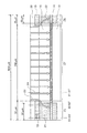
図1は、半導体レーザ装置1を示す斜視図である。
半導体レーザ装置1は、n型半導体基板11、n型バッファ層12、n型クラッド層13、量子井戸型活性層14、p型第1クラッド層15、エッチング停止層16、p型第2クラッド層17、p型キャップ層18、電流ブロック層19、及びp型コンタクト層20が、この順に積層されてなる。見易さのため、p型コンタクト層20を透明に描いている。
A semiconductor laser device according to an embodiment of the present invention will be described with reference to the drawings.
(Construction)
FIG. 1 is a perspective view showing a
The
n型クラッド層13からp型第2クラッド層17までが光導波路を構成し、当該光導波路の光出射端面(紙面手前)と反対側端面とには図示しない反射膜がコーティングされ、光共振器を構成する。
光出射端面側の反射膜の反射率は、反対側の反射膜の反射率よりも低く形成される。これにより、光出射端面から強いレーザ光が出射され、反対側端面からは微弱なレーザ光が出射される。前者は主用途に利用され、後者は受光素子で受光され前者の出力強度のモニタとして利用される。
The n-
The reflectance of the reflective film on the light emitting end face side is formed lower than the reflectance of the reflective film on the opposite side. Thereby, strong laser light is emitted from the light emitting end face, and weak laser light is emitted from the opposite end face. The former is used for main purposes, and the latter is received by a light receiving element and used as a monitor of the former output intensity.
光導波路の両端面からそれぞれ所定の長さまでの領域は、不純物(例えばZn)の拡散によって無秩序化し、内部に比べて禁制帯幅(エネルギーバンドギャップ)を大きくした窓領域21及び22が設けられる。
p型第2クラッド層17とp型キャップ層18とは、光共振器長方向にリッジ状に延設される。
The regions from the both end faces of the optical waveguide to predetermined lengths are disordered by diffusion of impurities (for example, Zn), and
The p-type
電流ブロック層19は、当該リッジの両脇、並びに、前記光導波路において窓領域21を包含する第1領域上、及び窓領域22を包含する第2領域上に形成される。
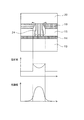
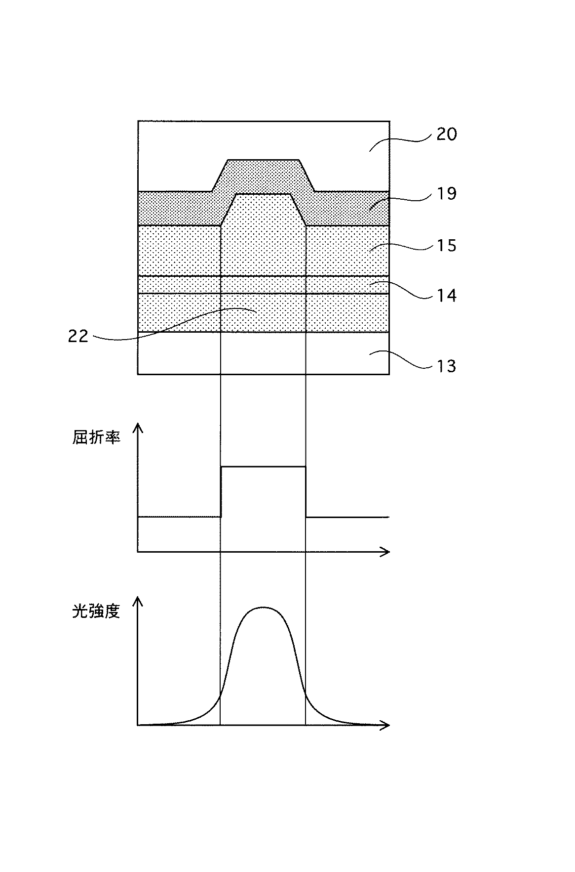
図2は、半導体レーザ装置1のX1−X1’断面を示す断面図であり、量子井戸型活性層14の詳細な構造が示される。
量子井戸型活性層14は、アンドープガイド層141、アンドープウェル層142、アンドープバリア層143、アンドープウェル層144、アンドープバリア層145、アンドープウェル層146、及びアンドープガイド層147が、この順に積層されてなる。
The
FIG. 2 is a cross-sectional view showing the X1-X1 ′ cross section of the
The quantum well
本実施の形態における各層の好適な膜厚、組成、キャリア濃度を表1に示す。 Table 1 shows the preferred film thickness, composition, and carrier concentration of each layer in this embodiment.
窓領域とそれを覆う電流ブロック層とに、光導波路の端面の光学的破壊(COD:Catastrophic Optical Damage)を防止する機能があることは従来から知られている。COD防止のため、半導体レーザ装置の両端面それぞれから略同一の大きさに、窓領域とそれを覆う電流ブロック層とを対称に設ける技術は周知である。
It has been conventionally known that the window region and the current blocking layer covering the window region have a function of preventing optical damage (COD: Catastrophic Optical Damage) of the end face of the optical waveguide. In order to prevent COD, a technique of providing a window region and a current blocking layer covering the window region so as to be approximately the same size from both end faces of the semiconductor laser device is well known.
半導体レーザ装置1では、さらに、光出射端面側の窓領域を覆う電流ブロック層の長さを、拡散によってキャリアが1/e(eは自然対数の底)に減少する距離を基準にして定めることによって、出射されるレーザ光の水平広がり角を管理することを特徴とする。
典型的には、当該電流ブロック層の長さを、光共振器の電流ブロック層で覆われない領域(利得領域)の長さの4%以上としてもよい。
In the
Typically, the length of the current blocking layer may be 4% or more of the length of the region (gain region) not covered with the current blocking layer of the optical resonator.
発明者らは、半導体レーザ装置1が、この構成によって、従来よりも大きな水平拡がり角θ‖を持ったレーザ光が得られることを確認した。その作用と特性データを後に詳述する。
(半導体レーザ装置1の製造方法)
半導体レーザ装置1の形状は、従来の典型的なリッジ型半導体レーザ装置と類似しているため、周知の方法で製造することができる。例えば、次のように製造してもよい。
The inventors confirmed that the
(Method for Manufacturing Semiconductor Laser Device 1)
Since the shape of the
n型半導体基板11上に、n型バッファ層12からp型キャップ層18までを成長させた後、両端部に不純物(例えばZn)を拡散させ、前記窓領域を形成する。次に、全面にSiO2などの誘電体絶縁膜を形成し、ホトリソグラフィーにより、前記リッジの上面となるべき帯状領域のみSiO2を残し、当該帯状領域の両側のp型第2クラッド層17とp型キャップ層18とをエッチングする。そして、当該帯状領域の光出射端側の誘電体膜を反対側の誘電体膜よりも大きく除去し、残ったSiO2をマスクとして電流ブロック層19を選択成長させる。最後に全ての誘電体膜を除去して、p型コンタクト層20を成長させる。
(ビーム整形領域とその作用)
半導体レーザ装置1が、前述した形状によって、従来よりも大きな水平拡がり角θ‖を持ったレーザ光を出射する作用について説明する。
After growing the n-
(Beam shaping area and its action)
The operation in which the
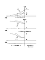
図3は、当該半導体レーザ装置のZ−Z’断面におけるキャリア(正孔)の流れを示す概念図であり、Z−Z’断面に見られる主要部を示している。紙面の左が光出射端面である。
ここで、半導体レーザ装置1において、電流ブロック層19に覆われn型コンタクト層20から直接には電流を注入されない光導波路の領域を、電流非注入領域と呼ぶ。以降、光出射端面側の電流非注入領域を、その作用からビーム整形領域と呼んで区別する。
FIG. 3 is a conceptual diagram showing the flow of carriers (holes) in the ZZ ′ section of the semiconductor laser device, and shows the main part seen in the ZZ ′ section. The left side of the drawing is the light exit end face.
Here, in the
図示したように、光導波路は、光出射端面から35μmまでのビーム整形領域25、反対側端面から25μmまでの電流非注入領域26、及びそれ以外の利得領域27に区分され、利得領域長は740μmである。この例では、窓領域21はビーム整形領域25に含まれ、窓領域22は電流非注入領域26に含まれる。
窓領域21の長さがビーム整形領域25の長さに比べて、短くなるほど吸収が大きくなってしきい値電流が増加し、長くなるほど窓領域21に電流が流れ込みCODレベルの低下を招く。そのため、窓領域21の長さはビーム整形領域25の長さの±20μm、望ましくは±10μmの範囲内である。
As shown in the figure, the optical waveguide is divided into a
As the length of the
図3において、外部からの電界は光共振器長に直交する方向に印加されている。利得領域27においてキャリアはその電界方向に沿って流れている(矢印24)。利得領域27の端部に注入されたキャリアは、窓領域21が不純物の拡散によって低抵抗化されている影響を受け、ビーム整形領域25及び窓領域21の内部にまで広がって流れる。
共振器長方向に移動するキャリア、すなわち、ビーム整形領域25へ流れ込んだキャリア(矢印23)は外部からの電界ではなく、拡散によって移動している。ビーム整形領域25におけるキャリアの濃度は、利得領域27から離れるに従って指数関数的に減少する。
In FIG. 3, the electric field from the outside is applied in the direction orthogonal to the optical resonator length. In the
Carriers that move in the resonator length direction, that is, carriers that flow into the beam shaping region 25 (arrows 23) are not diffused by the electric field from the outside but are moved by diffusion. The carrier concentration in the
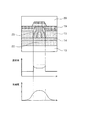
図4は、X1−X1’断面におけるキャリアの流れ、並びに、対応する位置における活性層の屈折率及び近視野像の光強度を示す概念図である。
X1−X1’断面におけるp型クラッド層及びn型クラッド層は低抵抗化(窓化)されていないので、キャリアの拡がりは小さくリッジ幅の中央付近を集中して流れる。活性層14の屈折率は、キャリアが注入されるとプラズマ効果によって低下し、屈折率が低下した領域では光閉じ込めが弱まることが知られているが、この断面において光閉じ込めが弱まる領域はリッジ幅の中央付近に限られ、近視野像の光強度はリッジ幅の中央に比較的よく集中する。
FIG. 4 is a conceptual diagram showing the carrier flow in the X1-X1 ′ section, and the refractive index of the active layer and the light intensity of the near-field image at the corresponding position.
Since the p-type cladding layer and the n-type cladding layer in the X1-X1 ′ cross section are not reduced in resistance (windowed), the carrier spread is small and flows concentrically near the center of the ridge width. It is known that the refractive index of the
図5は、X2−X2’断面におけるキャリアの流れ、並びに、対応する位置における活性層の屈折率及び近視野像の光強度を示す概念図である。
X2−X2’断面におけるp型クラッド層及びn型クラッド層は低抵抗化(窓化)されているので、利得領域の端部から流れ込んだキャリアが、リッジ幅の全体に広がって流れる。このため、屈折率の低下によって光閉じ込めが弱まる領域はリッジ幅の全体に渡り、近視野像の光強度は広範囲に広がる。
FIG. 5 is a conceptual diagram showing the carrier flow in the X2-X2 ′ section, and the refractive index of the active layer and the light intensity of the near-field image at the corresponding position.
Since the p-type clad layer and the n-type clad layer in the X2-X2 ′ cross section are reduced in resistance (windowed), carriers flowing from the end of the gain region flow in the entire ridge width. For this reason, the region where the light confinement is weakened due to the decrease in the refractive index extends over the entire ridge width, and the light intensity of the near-field image spreads over a wide range.
図6は、X3−X3’断面におけるキャリアの流れ、並びに、対応する位置における活性層の屈折率及び近視野像の光強度を示す概念図である。
X3−X3’断面におけるp型クラッド層及びn型クラッド層は低抵抗化(窓化)されているが、利得領域の端部から流れ込んだキャリアは、この断面には到達しない。そのため、この断面において光閉じ込めが弱まる領域は存在せず、近視野像の光強度はリッジ幅の中央に強く集中する。
FIG. 6 is a conceptual diagram showing the carrier flow in the X3-X3 ′ cross section, and the refractive index of the active layer and the light intensity of the near-field image at the corresponding position.
The p-type clad layer and the n-type clad layer in the X3-X3 ′ cross section are reduced in resistance (windowed), but carriers flowing from the end of the gain region do not reach this cross section. Therefore, there is no region where light confinement weakens in this cross section, and the light intensity of the near-field image is strongly concentrated in the center of the ridge width.
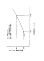
図7は、ビーム整形領域25内の電流、屈折率、及び遠視野像の水平広がり角のそれぞれと利得領域からの距離との関係を、利得領域の2種類の長さについて示すグラフである。利得領域が長くなる程、グラフは白抜き矢印の方向へシフトする。
前述したように、ビーム整形領域25内の電流は利得領域27からの距離に従って指数関数的に減少し、それに伴って、屈折率及び遠視野像の水平広がり角が図示した特性を示す。
FIG. 7 is a graph showing the relationship between the current in the
As described above, the current in the
ここで、キャリアが1/e(eは自然対数の底)に減少する距離を電流拡散距離l0とし、ビーム整形領域の長さを電流拡散距離よりも長くすることによって、光出射端面側へ到達するキャリア濃度を減少させ、実効屈折率低下による光閉じ込め低下を防止できる。これによって、光出射端面における近視野像の光強度がリッジ幅の中央に強く集中し、大きな水平拡がり角θ‖を持ったレーザ光が出射される。 Here, the distance at which the carriers are reduced to 1 / e (e is the base of the natural logarithm) is defined as the current diffusion distance l 0, and the length of the beam shaping region is made longer than the current diffusion distance, thereby moving toward the light emitting end face side. The carrier concentration that reaches can be reduced, and the optical confinement can be prevented from lowering due to the lowering of the effective refractive index. As a result, the light intensity of the near-field image at the light emitting end face is concentrated strongly at the center of the ridge width, and laser light having a large horizontal divergence angle θ‖ is emitted.
電流拡散距離l0は、利得領域長L、リッジ幅W、クラッド層の抵抗率ρによって決定され、
l0=2W/(βρI0)
で与えられる。ここで、βは接合パラメータと呼ばれ、室温では19.3C/Jである。I0は次式で与えられる。
The current diffusion distance l 0 is determined by the gain region length L, the ridge width W, the resistivity ρ of the cladding layer,
l 0 = 2W / (βρI 0 )
Given in. Here, β is called a bonding parameter and is 19.3 C / J at room temperature. I 0 is given by:
I0=Wβρ(√(1+WβρI/(2L))−1)/(2L)
ここで、Iは全注入電流である。
図8は、一つの典型例として、W=3μm、ρ=5Ω、I=100mAのときの利得領域長Lに対する電流拡散距離l0を示すグラフである。L=740μmでl0=約29μm(利得領域長の3.9%)、L=1030μmでl0=40μm(利得領域長の3.9%)となり、利得領域長Lが長くなる程、電流拡散距離l0も長くなる。
I 0 = Wβρ (√ (1 + WβρI / (2L))-1) / (2L)
Here, I is the total injection current.
FIG. 8 is a graph showing the
大きな水平拡がり角θ‖を持ったレーザ光を得るために、典型的には、ビーム整形領域の長さを利得領域長の4%以上にするとよい。なお、光出射端面と反対側端面における電流非注入領域の長さは出射光の水平拡がり角θ‖に影響を与えないので、COD防止のために必要な長さ(10μm以上)あればいくらでもよい。
図9は、しきい値電流及びCODレベルそれぞれの、ビーム整形領域長から窓領域長を減じた値に対する傾向を示すグラフであり、図3に示した半導体レーザ装置の窓領域21とビーム整形領域25との長さの関係を変えた場合を例示している。窓領域21の長さがビーム整形領域25の長さに比べて、短くなるほど吸収が大きくなってしきい値電流が増加し、長くなるほど窓領域に電流が流れ込みCODレベルの低下を招くため、窓領域21の長さをビーム整形領域25の長さの±10μmの範囲内とするのが望ましい。
(特性)
発明者らは、図3及び表1に示した断面構造を有し、利得領域長を一定にした
上で、光出射端面と反対側端面の電流非注入領域長が異なる複数の半導体レーザ装置を作成した。当該半導体レーザ装置を用いた実験によって得られた各種特性のデータを以下に示す。
In order to obtain a laser beam having a large horizontal divergence angle θ 典型, typically, the length of the beam shaping region should be 4% or more of the gain region length. Note that the length of the current non-injection region on the opposite end face to the light exit end face does not affect the horizontal spread angle θ‖ of the exit light, so that it can be any length as long as it is necessary to prevent COD (10 μm or more). .
FIG. 9 is a graph showing the tendency of the threshold current and the COD level with respect to the value obtained by subtracting the window region length from the beam shaping region length. The
(Characteristic)
The inventors have a plurality of semiconductor laser devices having the cross-sectional structure shown in FIG. 3 and Table 1 and having a constant gain region length and different current non-injection region lengths on the opposite end surface from the light emitting end surface. Created. Data of various characteristics obtained by experiments using the semiconductor laser device are shown below.
図10はチップ共振器長800μm、利得領域長740μmの場合の、ビーム整形領域長−CODレベル及びキンクレベル特性を示すグラフである。
図示したように、光出射端面のビーム整形領域長は、CODレベル及びキンクレベルの何れにも、ほとんど関与しないことを確認した。
図11は、チップ共振器長800μm、利得領域長740μmの場合の、
ビーム整形領域長−水平拡がり角特性を示すグラフである。
FIG. 10 is a graph showing beam shaping region length-COD level and kink level characteristics when the chip resonator length is 800 μm and the gain region length is 740 μm.
As shown in the figure, it was confirmed that the beam shaping region length of the light emitting end face hardly participates in both the COD level and the kink level.
FIG. 11 shows a case where the chip resonator length is 800 μm and the gain region length is 740 μm.
It is a graph which shows the beam shaping area | region length-horizontal divergence angle characteristic.
図示したように、光出射端面のビーム整形領域長を35μm以上とした場合に、(1)30mW及び5mWの何れの光出力時にも、水平拡がり角が約1度広がること、及び(2)光出射端面のビーム整形領域長を35μm以上とした場合に、光出力を変えた場合の水平拡がり角の変動が抑制されることを確認した。
図12は利得領域長1030μmの場合の、ビーム整形領域長−水平拡がり角特性を示すグラフである。
As shown in the figure, when the beam shaping region length of the light emitting end face is 35 μm or more, (1) the horizontal divergence angle is expanded by about 1 degree at any light output of 30 mW and 5 mW, and (2) light It was confirmed that when the beam shaping region length of the emission end face is 35 μm or more, the fluctuation of the horizontal divergence angle when the light output is changed is suppressed.
FIG. 12 is a graph showing the beam shaping region length-horizontal divergence angle characteristic when the gain region length is 1030 μm.
図示したように、光出射端面のビーム整形領域長を50μm以上とした場合に、(1)70mW及び5mWの何れの光出力時にも、水平拡がり角が約0.6度広がること、及び(2)光出射端面のビーム整形領域長を50μm以上とした場合に、光出力を変えた場合の水平拡がり角の変動が抑制されることを確認した。
図13は、ビーム整形領域長−非点収差特性を示すグラフである。
As shown in the figure, when the beam shaping area length of the light emitting end face is set to 50 μm or more, (1) the horizontal divergence angle is expanded by about 0.6 degrees at any light output of 70 mW and 5 mW, and (2 ) It was confirmed that when the beam shaping area length of the light emitting end face is 50 μm or more, the fluctuation of the horizontal divergence angle when the light output is changed is suppressed.
FIG. 13 is a graph showing the beam shaping area length-astigmatism characteristics.
図示したように、ビーム整形領域長は、光出力を変えた場合の非点収差の変動にほとんど関与しないことを確認した。
チップ共振器長800μmのレーザを例に挙げると、これらの特性データは、望ましいCODレベル及びキンクレベルが得られるよう、半導体レーザ装置の断面構造と利得領域の長さとを好適に設計した上で、それとは独立して、光出射端面のビーム整形領域の長さを30μm以上とすれば、当該CODレベル及びキンクレベルを損なうことなく、従来よりも大きな水平拡がり角を持ったレーザ光が得られることを示している。
As shown in the figure, it was confirmed that the beam shaping region length hardly participates in the fluctuation of astigmatism when the light output is changed.
Taking a laser with a chip resonator length of 800 μm as an example, these characteristic data are obtained by suitably designing the cross-sectional structure of the semiconductor laser device and the length of the gain region so as to obtain a desired COD level and kink level. Independently, if the length of the beam shaping region on the light emitting end face is 30 μm or more, laser light having a larger horizontal divergence angle than before can be obtained without impairing the COD level and kink level. Is shown.
また、光出射端面のビーム整形領域の長さを35μm以上とすれば、光出力に応じた水平拡がり角の変動が抑制され、光出力の最大値や光学系に関する設計マージンを縮小できることも示している。
このように、光出射端面のビーム整形領域の長さを管理することによって、断面構造と利得領域の長さとに依存する各種特性とは独立してレーザ光の水平拡がり角が管理可能となること、及び光出力に応じた水平拡がり角の変動が抑制されることによって、半導体レーザ装置の設計が合理化され、その結果、良好な特性の半導体レーザ装置を従来よりも簡明に設計することが可能となる。
(2波長半導体レーザ装置への適用例)
図14は、本発明を適用した2波長半導体レーザ装置3を示す斜視図である。
It also shows that if the length of the beam shaping area on the light exit end face is 35 μm or more, the fluctuation of the horizontal divergence angle according to the light output is suppressed, and the maximum value of the light output and the design margin concerning the optical system can be reduced. Yes.
In this way, by managing the length of the beam shaping region at the light emitting end face, the horizontal divergence angle of the laser beam can be managed independently of various characteristics depending on the cross-sectional structure and the length of the gain region. In addition, by suppressing the fluctuation of the horizontal divergence angle according to the light output, the design of the semiconductor laser device is rationalized, and as a result, it is possible to design a semiconductor laser device with good characteristics more easily than before. Become.
(Application example to a two-wavelength semiconductor laser device)
FIG. 14 is a perspective view showing a two-wavelength
2波長半導体レーザ装置3は、単一のn-GaAs基板上に、モノリシック集積化プロセスを用いて、AlGaAs系の赤外半導体レーザ装置31と、InGaAlP系の赤色半導体レーザ装置32とが形成されてなる。
2波長半導体レーザ装置3は、赤外半導体レーザ装置31及び赤色半導体レーザ装置32の一方又は両方において、光出射端面側に電流拡散距離よりも大きなビーム整形領域が設けられることを特徴とする。
In the two-wavelength
The two-wavelength
なお、モノリシック集積化プロセスを用いた2波長半導体レーザ装置の製造方法は、例えば、特開2001−217504号公報に開示されている。
(溝型半導体レーザ装置への適用例)
図15は、本発明を適用した溝型半導体レーザ装置4を示す斜視図である。
溝型半導体レーザ装置4は、GaAs基板41、バッファ層42、n型第1クラッド層43、n型第2クラッド層44、量子井戸型活性層45、p型第1クラッド層46、p型第2クラッド層47、電流ブロック層48、p型第3クラッド層49、及びコンタクト層50が、この順に積層されてなる。見易さのため、p型第3クラッド層49、及びコンタクト層50を透明に描いている。
A method for manufacturing a two-wavelength semiconductor laser device using a monolithic integration process is disclosed in, for example, Japanese Patent Application Laid-Open No. 2001-217504.
(Application example to groove type semiconductor laser device)
FIG. 15 is a perspective view showing a groove type semiconductor laser device 4 to which the present invention is applied.
The trench type semiconductor laser device 4 includes a
n型第1クラッド層43からp型第3クラッド層49までが光導波路を構成し、当該光導波路の光出射端面(紙面手前)と反対側端面とには図示しない反射膜がコーティングされ、光共振器を構成する。
光導波路の両端面からそれぞれ所定の長さまでの領域51及び52は、無秩序化により窓領域とされる。
The n-type
電流ブロック層48は、p型第2クラッド層47とp型第3クラッド層49との間の、光共振器の全長にわたる帯状領域の中央部を除外した領域に埋設される。
図示したように、利得領域長は740μmである。光共振器の光出射端面から35μmまでの領域、及び反対側端面から25μmまでの領域には、電流ブロック層48が埋設され、光出射端面側の電流非注入領域にビーム整形作用が与えられる。
(青紫色半導体レーザ装置への適用例)
図16は、本発明を適用した青紫色半導体レーザ装置6を示す斜視図である。
The
As shown, the gain region length is 740 μm. A
(Application example to blue-violet semiconductor laser device)
FIG. 16 is a perspective view showing a blue-violet semiconductor laser device 6 to which the present invention is applied.
青紫色半導体レーザ装置6は、n型GaN基板61、n型AlGaNクラッド層62、量子井戸型活性層63、p型AlGaNクラッド層64、電流ブロック層65、p型GaNコンタクト層66が、この順に積層されてなる。見易さのため、p型GaNコンタクト層66を透明に描いている。
n型AlGaNクラッド層62からp型AlGaNクラッド層64までが光導波路を構成し、当該光導波路の光出射端面(紙面手前)と反対側端面とには図示しない反射膜がコーティングされ、光共振器を構成する。
The blue-violet semiconductor laser device 6 includes an n-
The n-type
光導波路の両端面からそれぞれ所定の長さまでの領域67及び68は、無秩序化により窓領域とされる。
図示したように、青紫色半導体レーザ装置6における利得領域長は730μmである。光共振器の光出射端面から40μmまでの領域、及び反対側端面から
30μmまでの領域には、電流ブロック層65が覆設され、光出射端面側の電流非注入領域にビーム整形作用が与えられる。
As shown in the drawing, the gain region length in the blue-violet semiconductor laser device 6 is 730 μm. A
本発明に係る半導体レーザ装置は、例えば光ディスク装置における光ピックアップに利用できる。 The semiconductor laser device according to the present invention can be used for an optical pickup in an optical disc device, for example.
1 半導体レーザ装置
3 2波長半導体レーザ装置
4 溝型半導体レーザ装置
6 青紫色半導体レーザ装置
11 n型半導体基板
12 n型バッファ層
13 n型クラッド層
14 量子井戸型活性層
15 p型第1クラッド層
16 エッチング停止層
17 p型第2クラッド層
18 p型キャップ層
19 電流ブロック層
20 p型コンタクト層
21、22 窓領域
23、24 キャリアの流れ
25 ビーム整形領域
26 電流非注入領域
27 利得領域
31 赤外半導体レーザ装置
32 赤色半導体レーザ装置
41 GaAs基板
42 バッファ層
43 n型第1クラッド層
44 n型第2クラッド層
45 量子井戸型活性層
46 p型第1クラッド層
47 p型第2クラッド層
48 電流ブロック層
49 p型第3クラッド層
50 コンタクト層
51、52 窓領域
61 n型GaN基板
62 n型AlGaNクラッド層
63 量子井戸型活性層
64 p型AlGaNクラッド層
65 電流ブロック層
66 p型GaNコンタクト層
67、68 窓領域
141、147 アンドープガイド層
142、144、146 アンドープウェル層
143、145 アンドープバリア層
147 アンドープガイド層
DESCRIPTION OF
Claims (3)
前記光共振器の、光出射端面から第1の長さまでに至る第1領域、及び反対側端面から第2の長さまでに至る第2領域それぞれにおける前記第2導電型のクラッド層上に形成された電流ブロック層と
を備え、
前記活性層の、前記光出射端面及び前記反対側端面からそれぞれ所定の長さまでに至る部分は、他の部分に比べてより大きな禁制帯幅を持つように形成されており、
前記光共振器の前記第1領域及び前記第2領域を除外した第3領域から前記第1領域へ流れ込む電流が拡散によって1/e(eは自然対数の底)に減少する距離よりも、前記第1の長さを長くすることによって、出射光の水平広がり角を管理することを特徴とする半導体レーザ装置。 An optical resonator in which both end faces of an optical waveguide formed by laminating a first conductivity type cladding layer, an active layer, and a second conductivity type cladding layer in this order are used as a pair of reflection surfaces;
The optical resonator is formed on the second conductivity type cladding layer in each of the first region extending from the light emitting end surface to the first length and the second region extending from the opposite end surface to the second length. Current blocking layer and
The part of the active layer from the light emitting end face and the opposite end face to a predetermined length is formed to have a larger forbidden band width compared to other parts,
More than the distance by which the current flowing from the third region excluding the first region and the second region of the optical resonator to the first region is reduced to 1 / e (e is the base of natural logarithm) by diffusion. A semiconductor laser device characterized in that the horizontal spread angle of emitted light is managed by increasing the first length.
ことを特徴とする請求項1に記載の半導体レーザ装置。 The semiconductor laser device according to claim 1, wherein the first length is 4% or more of the length of the third region.
ことを特徴とする請求項1に記載の半導体レーザ装置。 A portion of the active layer from the light emitting end face to a length included in a range of ± 20 μm of the first length is formed to have the forbidden band width. The semiconductor laser device according to claim 1.
Priority Applications (3)
| Application Number | Priority Date | Filing Date | Title |
|---|---|---|---|
| JP2004107783A JP4136988B2 (en) | 2004-03-31 | 2004-03-31 | Semiconductor laser device |
| CNA2004101024029A CN1677777A (en) | 2004-03-31 | 2004-12-22 | A semiconductor laser |
| US11/070,267 US7197055B2 (en) | 2004-03-31 | 2005-03-03 | Semiconductor laser |
Applications Claiming Priority (1)
| Application Number | Priority Date | Filing Date | Title |
|---|---|---|---|
| JP2004107783A JP4136988B2 (en) | 2004-03-31 | 2004-03-31 | Semiconductor laser device |
Publications (2)
| Publication Number | Publication Date |
|---|---|
| JP2005294544A true JP2005294544A (en) | 2005-10-20 |
| JP4136988B2 JP4136988B2 (en) | 2008-08-20 |
Family
ID=35050151
Family Applications (1)
| Application Number | Title | Priority Date | Filing Date |
|---|---|---|---|
| JP2004107783A Expired - Fee Related JP4136988B2 (en) | 2004-03-31 | 2004-03-31 | Semiconductor laser device |
Country Status (3)
| Country | Link |
|---|---|
| US (1) | US7197055B2 (en) |
| JP (1) | JP4136988B2 (en) |
| CN (1) | CN1677777A (en) |
Families Citing this family (11)
| Publication number | Priority date | Publication date | Assignee | Title |
|---|---|---|---|---|
| WO2006102686A2 (en) * | 2005-03-25 | 2006-09-28 | Trumpf Photonics Inc. | High power diode lasers |
| KR20060122615A (en) * | 2005-05-27 | 2006-11-30 | 삼성전자주식회사 | Nitride-based semiconductor laser diode and manufacturing method thereof |
| JP2008226378A (en) * | 2007-03-14 | 2008-09-25 | Matsushita Electric Ind Co Ltd | Semiconductor device, manufacturing method thereof, and optical pickup module |
| EP2346124B1 (en) * | 2008-10-31 | 2018-09-19 | Optoenergy, Inc. | Semiconductor laser element |
| US9847372B2 (en) | 2011-12-01 | 2017-12-19 | Micron Technology, Inc. | Solid state transducer devices with separately controlled regions, and associated systems and methods |
| CN103956647A (en) * | 2014-05-16 | 2014-07-30 | 深圳清华大学研究院 | Semiconductor laser chip and manufacturing method thereof |
| DE102015116335B4 (en) * | 2015-09-28 | 2024-10-24 | OSRAM Opto Semiconductors Gesellschaft mit beschränkter Haftung | semiconductor laser |
| US11777277B2 (en) * | 2018-09-12 | 2023-10-03 | Mitsubishi Electric Corporation | Semiconductor laser |
| CN115021071A (en) * | 2020-06-09 | 2022-09-06 | 厦门市三安光电科技有限公司 | Laser diode and manufacturing method thereof |
| CN112290384A (en) * | 2020-12-29 | 2021-01-29 | 江西铭德半导体科技有限公司 | Edge-emitting high-power laser and manufacturing method thereof |
| CN114583556B (en) * | 2022-05-05 | 2022-07-15 | 苏州长光华芯光电技术股份有限公司 | A vertical carrier modulation high-power semiconductor light-emitting chip and preparation method thereof |
Family Cites Families (2)
| Publication number | Priority date | Publication date | Assignee | Title |
|---|---|---|---|---|
| JP2624881B2 (en) * | 1990-08-23 | 1997-06-25 | 株式会社東芝 | Semiconductor laser device and method of manufacturing the same |
| JP2003078203A (en) | 2001-09-06 | 2003-03-14 | Kenwood Corp | Laser modulation control device, laser modulation control method and program thereof |
-
2004
- 2004-03-31 JP JP2004107783A patent/JP4136988B2/en not_active Expired - Fee Related
- 2004-12-22 CN CNA2004101024029A patent/CN1677777A/en active Pending
-
2005
- 2005-03-03 US US11/070,267 patent/US7197055B2/en not_active Expired - Lifetime
Also Published As
| Publication number | Publication date |
|---|---|
| CN1677777A (en) | 2005-10-05 |
| US20050232325A1 (en) | 2005-10-20 |
| JP4136988B2 (en) | 2008-08-20 |
| US7197055B2 (en) | 2007-03-27 |
Similar Documents
| Publication | Publication Date | Title |
|---|---|---|
| JP2010267731A (en) | Nitride semiconductor laser device | |
| JP4136988B2 (en) | Semiconductor laser device | |
| JP3926313B2 (en) | Semiconductor laser and manufacturing method thereof | |
| TW200814479A (en) | Semiconductor laser device | |
| CN101741016A (en) | Semiconductor laser and manufacturing process thereof | |
| JP4472278B2 (en) | Semiconductor laser element | |
| JP2005033077A (en) | Semiconductor laser device | |
| CN100388576C (en) | Semiconductor laser device and optical pickup device using the same | |
| KR100682971B1 (en) | Semiconductor laser device and manufacturing method thereof | |
| JP3779248B2 (en) | Semiconductor laser element | |
| CN1937338A (en) | Multi-wavelength semiconductor laser | |
| JP2007095758A (en) | Semiconductor laser | |
| US6842471B2 (en) | Semiconductor laser device having a current non-injection area | |
| JP2006294984A (en) | Semiconductor laser device, method for manufacturing the same, and optical pickup device using the same | |
| JP4317357B2 (en) | Semiconductor laser device and manufacturing method thereof | |
| US20100309941A1 (en) | Semiconductor laser device | |
| US20060140236A1 (en) | Semiconductor laser device and optical pick-up device using the same | |
| JP4138731B2 (en) | Semiconductor laser device and manufacturing method thereof | |
| JP2012104766A (en) | Semiconductor laser device | |
| WO1997041625A1 (en) | Semiconductor laser and method for manufacturing the same | |
| JP2012114357A (en) | Semiconductor laser | |
| JP2007142227A (en) | Semiconductor laser device | |
| JP2006196846A (en) | Multi-wavelength semiconductor laser device | |
| JP2010232614A (en) | Semiconductor laser and manufacturing method thereof | |
| JP2002223038A (en) | Semiconductor laser device |
Legal Events
| Date | Code | Title | Description |
|---|---|---|---|
| A621 | Written request for application examination |
Free format text: JAPANESE INTERMEDIATE CODE: A621 Effective date: 20060602 |
|
| A977 | Report on retrieval |
Free format text: JAPANESE INTERMEDIATE CODE: A971007 Effective date: 20070409 |
|
| A131 | Notification of reasons for refusal |
Free format text: JAPANESE INTERMEDIATE CODE: A131 Effective date: 20080115 |
|
| A521 | Request for written amendment filed |
Free format text: JAPANESE INTERMEDIATE CODE: A523 Effective date: 20080313 |
|
| TRDD | Decision of grant or rejection written | ||
| A01 | Written decision to grant a patent or to grant a registration (utility model) |
Free format text: JAPANESE INTERMEDIATE CODE: A01 Effective date: 20080507 |
|
| A01 | Written decision to grant a patent or to grant a registration (utility model) |
Free format text: JAPANESE INTERMEDIATE CODE: A01 |
|
| A61 | First payment of annual fees (during grant procedure) |
Free format text: JAPANESE INTERMEDIATE CODE: A61 Effective date: 20080603 |
|
| R150 | Certificate of patent or registration of utility model |
Free format text: JAPANESE INTERMEDIATE CODE: R150 Ref document number: 4136988 Country of ref document: JP Free format text: JAPANESE INTERMEDIATE CODE: R150 |
|
| FPAY | Renewal fee payment (event date is renewal date of database) |
Free format text: PAYMENT UNTIL: 20110613 Year of fee payment: 3 |
|
| FPAY | Renewal fee payment (event date is renewal date of database) |
Free format text: PAYMENT UNTIL: 20120613 Year of fee payment: 4 |
|
| FPAY | Renewal fee payment (event date is renewal date of database) |
Free format text: PAYMENT UNTIL: 20120613 Year of fee payment: 4 |
|
| FPAY | Renewal fee payment (event date is renewal date of database) |
Free format text: PAYMENT UNTIL: 20130613 Year of fee payment: 5 |
|
| S533 | Written request for registration of change of name |
Free format text: JAPANESE INTERMEDIATE CODE: R313533 |
|
| R350 | Written notification of registration of transfer |
Free format text: JAPANESE INTERMEDIATE CODE: R350 |
|
| S111 | Request for change of ownership or part of ownership |
Free format text: JAPANESE INTERMEDIATE CODE: R313113 |
|
| R350 | Written notification of registration of transfer |
Free format text: JAPANESE INTERMEDIATE CODE: R350 |
|
| R250 | Receipt of annual fees |
Free format text: JAPANESE INTERMEDIATE CODE: R250 |
|
| R250 | Receipt of annual fees |
Free format text: JAPANESE INTERMEDIATE CODE: R250 |
|
| LAPS | Cancellation because of no payment of annual fees |