JP2005294445A - Coil element - Google Patents
Coil element Download PDFInfo
- Publication number
- JP2005294445A JP2005294445A JP2004105839A JP2004105839A JP2005294445A JP 2005294445 A JP2005294445 A JP 2005294445A JP 2004105839 A JP2004105839 A JP 2004105839A JP 2004105839 A JP2004105839 A JP 2004105839A JP 2005294445 A JP2005294445 A JP 2005294445A
- Authority
- JP
- Japan
- Prior art keywords
- coil
- magnetic
- spiral
- laminated
- conductor
- Prior art date
- Legal status (The legal status is an assumption and is not a legal conclusion. Google has not performed a legal analysis and makes no representation as to the accuracy of the status listed.)
- Pending
Links
Images
Landscapes
- Electromagnets (AREA)
- Coils Or Transformers For Communication (AREA)
Abstract
【課題】発生した磁束を効果的に遮蔽して所望の場所に効果的に集中できて、比較的小さな構造でありながら所望の箇所に比較的大きな磁場を発生できるコイル素子を提供することである。
【解決手段】コイル素子は、渦巻き状の磁性体コイル2と渦巻き状の導体コイル3とが直接重なり接している積層コイル4を有する。積層コイル4は、絶縁性表面を有する平面基板1上に形成され得て、積層コイル4の外周部と中心部の少なくとも一方に、積層コイル4と電気的な接続のない少なくとも磁性体部分6からなる壁部5が形成されてもよい。
【選択図】図1To provide a coil element capable of effectively shielding a generated magnetic flux and effectively concentrating it at a desired location and generating a relatively large magnetic field at a desired location while having a relatively small structure. .
A coil element has a laminated coil 4 in which a spiral magnetic coil 2 and a spiral conductor coil 3 are in direct contact with each other. The laminated coil 4 can be formed on the flat substrate 1 having an insulating surface, and at least one of the outer peripheral portion and the central portion of the laminated coil 4 is provided with at least a magnetic part 6 that is not electrically connected to the laminated coil 4. A wall portion 5 may be formed.
[Selection] Figure 1
Description
本発明は、コイル素子、これを用いたアクチュエータなどの装置に関するものである。 The present invention relates to a coil element and an apparatus such as an actuator using the coil element.
近年、電子機器は年を追うごとに小型化、薄型化する傾向にある。これに伴って回路基板等上の配線も高密度化する傾向にあり、種々の方法を用いた微細配線及びその作製方法が提案されつつある。電子機器に搭載するインダクタンス部品においても、小型化、薄膜化が要求されている。このことは駆動系を有する電子機器も例外ではなく、駆動部の小型化、薄型化は必須条件となり、インダクタ、トランス等の磁性部品の小型化、薄型化も要求されてきている。こうした要求に対して、従来のフェライトコアに巻線を施した巻線方式のコイルの小型化には限界があり、従って、その要求を満足すべく、現在、平面コイルが提案されている。 In recent years, electronic devices tend to be smaller and thinner as the years progress. Along with this, wirings on circuit boards and the like tend to be denser, and fine wirings using various methods and manufacturing methods thereof are being proposed. Inductance components mounted on electronic devices are also required to be smaller and thinner. This is not an exception for electronic devices having a drive system, and it is indispensable to reduce the size and thickness of the drive unit, and to reduce the size and thickness of magnetic components such as inductors and transformers. In response to such demands, there is a limit to the miniaturization of a winding-type coil in which a conventional ferrite core is wound. Accordingly, a planar coil has been proposed to satisfy the demand.
従来の平面コイルとして、薄膜成膜技術とメッキ法を用いた平面コイル及びその作製方法が提案されている(特許文献1参照)。ここで開示の平面コイルは、薄膜成膜とエッチングで形成された第1のコイル導体上に第2のコイル導体がメッキにより形成され、コイル導体以外の部分がポリイミド或いはポリアミドからなる絶縁体で構成されている。 As a conventional planar coil, a planar coil using a thin film deposition technique and a plating method and a manufacturing method thereof have been proposed (see Patent Document 1). The planar coil disclosed here is composed of a first coil conductor formed by thin film deposition and etching, a second coil conductor formed by plating, and a portion other than the coil conductor made of an insulator made of polyimide or polyamide. Has been.
また、平面コイルは、メッキ等で形成されたものが一般的に知られている(特許文献2、特許文献3参照)。これらの平面コイルでは、層間絶縁層を介しコイルを多層化してコイルのターン数を大きくしインダクタンスを高くしている。
しかしながら、上記従来の平面コイルを、走査ミラー等を搭載した駆動装置に内蔵する構成では、コイル中心部付近における磁束密度を充分大きくすることは困難であり、そうした場所で高い起磁力を得るには通電電流を大きくする必要がある。そうすると、駆動装置自体の消費電力が高くなり、使用環境も制限され、例えば、モバイル機器中での使用は難しい。また、コイルを多層化してターン数を増やすにあたり、層間絶縁層として樹脂材料を使用すると、コイル素子デバイスを真空パッケージ化して可動部を空気抵抗なく小消費電力で駆動することが不可能になるという制約も生じてしまう。 However, it is difficult to sufficiently increase the magnetic flux density in the vicinity of the center of the coil in the configuration in which the above conventional planar coil is built in a driving device equipped with a scanning mirror or the like, and in order to obtain a high magnetomotive force in such a place. The energizing current needs to be increased. If it does so, the power consumption of drive device itself will become high, a use environment will also be restrict | limited, for example, use in a mobile device will be difficult. In addition, when a resin material is used as an interlayer insulating layer in order to increase the number of turns by increasing the number of turns of the coil, it becomes impossible to drive the movable part with low power consumption without air resistance by forming the coil element device into a vacuum package. Restrictions also arise.
上記課題に鑑み、本発明のコイル素子は、渦巻き状の磁性体コイルと渦巻き状の導体コイルとが直接重なり接している積層コイルを有することを特徴とする。また、本発明のコイル素子は、絶縁性表面を有する平面基板上に、渦巻き状の磁性体コイルが形成され、渦巻き状の磁性体コイル上に渦巻き状の導体コイルが直接接するように形成された積層コイルを有し、積層コイルの外周部と中心部の少なくとも一方に、積層コイルと電気的な接続のない少なくとも磁性体部分からなる壁部が形成されていることを特徴とする。 In view of the above problems, the coil element of the present invention is characterized by having a laminated coil in which a spiral magnetic coil and a spiral conductor coil are in direct contact with each other. The coil element of the present invention is formed such that a spiral magnetic coil is formed on a flat substrate having an insulating surface, and the spiral conductor coil is in direct contact with the spiral magnetic coil. It has a laminated coil, and at least one of the outer peripheral part and center part of a laminated coil is formed with the wall part which consists of an at least magnetic body part which is not electrically connected with a laminated coil.
また、上記課題に鑑み、本発明のアクチュエータは、上記コイル素子と、可動部と、可動部を支持する支持部とを有し、該コイル素子の発生する磁場により該可動部を駆動することを特徴とする。さらに、上記課題に鑑み、本発明の画像形成装置は、このアクチュエータと光源を有し、該光源からの光を該アクチュエータで偏向して所望の面に画像を形成することを特徴とする。 In view of the above problems, an actuator according to the present invention includes the coil element, a movable part, and a support part that supports the movable part, and the movable part is driven by a magnetic field generated by the coil element. Features. Further, in view of the above problems, the image forming apparatus of the present invention includes the actuator and a light source, and deflects light from the light source by the actuator to form an image on a desired surface.
本発明によれば、磁性体コイル、或いは少なくとも磁性体部を含む壁部により、発生した磁束を有効に遮蔽して所望の場所に有効に集中できるので、比較的小さな構造でありながら所望の箇所に比較的大きな磁場を発生できるコイル素子を提供できる。具体的には、磁束の漏れを防いで所望の場所における磁束密度を大きくでき、比較的断面積が大きくできるので比較的大きな電流が流せて起磁力を高くできるので、薄型化、小型化が容易で、層数を少なくできるコイル素子を実現できる。 According to the present invention, since the generated magnetic flux can be effectively shielded and concentrated at a desired location by the magnetic coil or the wall portion including at least the magnetic material portion, the desired location can be achieved while having a relatively small structure. A coil element capable of generating a relatively large magnetic field can be provided. Specifically, the magnetic flux density at a desired location can be increased by preventing magnetic flux leakage, and the cross-sectional area can be made relatively large, so that a relatively large current can flow and the magnetomotive force can be increased, making it easy to reduce the thickness and size. Thus, a coil element that can reduce the number of layers can be realized.
さらに具体的には、本発明により、コイル層数を増やすことによってターン数を大きくし、起磁力を大きくする必要が無くなり、デバイスの薄型化が実現できるコイル素子を薄型且つ小型で実現できた。また、ターン数を増やすことなく起磁力を高くできるのでコイル配線長自体を短くでき、コイル自体の抵抗を低くできて消費電力低減の効果を奏することができる。さらに、電磁アクチュエータ等のように駆動素子を駆動する電磁コイル素子として用いる場合においても、比較的小型でありながら十分な起磁力にて駆動素子を駆動させることが可能になった。 More specifically, according to the present invention, it is not necessary to increase the number of turns by increasing the number of coil layers and to increase the magnetomotive force, and the coil element capable of realizing a thin device can be realized thin and small. Further, since the magnetomotive force can be increased without increasing the number of turns, the coil wiring length itself can be shortened, the resistance of the coil itself can be lowered, and the effect of reducing power consumption can be achieved. Furthermore, even when used as an electromagnetic coil element for driving a drive element such as an electromagnetic actuator, the drive element can be driven with a sufficient magnetomotive force while being relatively small.
上記本発明の基本的な構成に基づく典型的な実施形態を以下に説明する。
典型的な形態では、絶縁性表面を有する平面基板上に、渦巻き状の磁性体コイルが形成され、渦巻き状の磁性体コイル上に渦巻き状の導体コイルが直接接するように形成された積層コイルを有し、積層コイルの外周部と中心部の少なくとも一方(両方に設ければ磁束収束の効果は大きくなる)に、積層コイルと電気的な接続のない少なくとも磁性体部分からなる壁部が形成されている。前記壁部が積層コイルと同時に形成できて作製を容易にする為には、壁部が、積層コイルと同じ積層構造で同じ材料の磁性体部分と導体材料部分からなるのがよい。コイルの厚みを比較的大きくして断面積を大きくする為には、磁性体コイルや導体コイルをメッキ膜からなる様にするとよい。
Exemplary embodiments based on the basic configuration of the present invention will be described below.
In a typical form, a spiral magnetic coil is formed on a flat substrate having an insulating surface, and a laminated coil formed so that the spiral conductor coil is in direct contact with the spiral magnetic coil. And at least one of the outer peripheral portion and the central portion of the laminated coil (if it is provided on both of them, the effect of converging the magnetic flux becomes larger) is formed with a wall portion made of at least a magnetic part that is not electrically connected to the laminated coil. ing. In order for the wall portion to be formed at the same time as the laminated coil and to facilitate manufacture, the wall portion is preferably composed of a magnetic material portion and a conductive material portion of the same material with the same laminated structure as the laminated coil. In order to increase the thickness of the coil and increase the cross-sectional area, it is preferable that the magnetic coil and the conductor coil be made of a plating film.
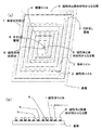
この様に、上記効果を奏する典型的なコイルの一つは、図1(a)、(b)に示すように、基板1上に磁性体コイル2(これは導体でもある)が形成されており、該磁性体コイル2上に、直接、導体コイル3が形成されて積層コイル4が構成されている。そして、磁性体コイル2と導体コイル3の外周部もしくは中心部に、積層コイル4と電気的な接続のない磁性体部分6と導体材料部分7からなる壁部5が形成されている。
In this way, one of typical coils having the above-described effect is that a magnetic coil 2 (which is also a conductor) is formed on a substrate 1 as shown in FIGS. 1 (a) and 1 (b). The conductor coil 3 is directly formed on the magnetic coil 2 to form a laminated coil 4. And the
磁性体コイル2は、周回した積層コイル4から発生する磁束密度を高める機能を備えている。すなわち、磁性体コイル2がなく導体コイル3のみであると磁性体コイル2による磁束の遮蔽効果がなくなって磁束が拡がってしまい、特に、コイル中心部における磁束密度が低減してしまう。導体コイル3下に磁性体コイル2を配置することで磁束の拡がりが抑制され、コイル中心部の上方の磁束密度を高められる。これにより、多層化によってコイルのターン数を増やす必要もなく、多層化に伴う層間絶縁層の形成も不要となり、薄型化が可能となる。 The magnetic coil 2 has a function of increasing the magnetic flux density generated from the laminated coil 4 that has been turned around. That is, if there is no magnetic coil 2 and only the conductor coil 3 is used, the magnetic flux shielding effect by the magnetic coil 2 is lost, and the magnetic flux expands. In particular, the magnetic flux density at the center of the coil is reduced. By disposing the magnetic coil 2 under the conductor coil 3, the spread of the magnetic flux is suppressed, and the magnetic flux density above the coil center can be increased. Thus, it is not necessary to increase the number of turns of the coil due to multilayering, and it is not necessary to form an interlayer insulating layer due to multilayering, and the thickness can be reduced.
さらに、コイルの外周部や中心部に、積層コイル4と電気的な接続のない磁性体部分6と導体材料部分7からなる壁部5を設けることによって、コイルから発生する磁束がコイル外周方向へ拡がってしまうのを抑制するとともにコイルの中心部に磁束を集中できて、コイル中心部上方の磁束密度を高められる。またさらに、積層コイル4上にも渦巻き状の磁性体コイルを、直接、接するように形成すれば、導体コイル3が上下の磁性体コイル2によって挟まれ、所望の場所に磁束をより収束させることができる。
Furthermore, by providing a
各構成要素には、以下の様な具体的態様が好適には採用可能である。
まず、基板材料としてはガラス、シリコン、石英、セラミック、樹脂、金属などを用いることが可能である。但し、磁性体コイル2が接触する表面は絶縁性表面となっている必要がある。磁性体コイル2、および磁性体と導体材料からなる壁部5の磁性体材料部分6には、高透磁率材料(軟磁性体)を用いる。典型的な材料としては、鉄−シリコン、鉄−ニッケル、マンガン−亜鉛フェライト、ニッケル−亜鉛フェライト等が挙げられる。
The following specific modes can be suitably employed for each component.
First, glass, silicon, quartz, ceramic, resin, metal, or the like can be used as the substrate material. However, the surface with which the magnetic coil 2 contacts must be an insulating surface. A high permeability material (soft magnetic material) is used for the magnetic material coil 2 and the
次に、導体コイル3の材料としては、比抵抗の小さい銅や金を用いるのが好適ではあるが、他の金属および合金を使用してもよい。コイルの配線は、幅に対して高さの方が大きいほど狭ピッチでも配線断面積が大きくとれ、配線抵抗を低く抑えることができる(尚、磁性体コイル2の部分もこの配線断面積の増大に寄与する)。従って、コイル配線は厚く形成する方がよいため、スパッタ成膜や蒸着といった薄膜プロセスでなく、厚膜化が容易なメッキで形成する方が好ましい。また、磁性体コイル2と導体コイル3は層間絶縁層を介することなく形成されているので、基板1に無機材料を選択すればコイル素子は脱ガスの殆ど無いデバイスを構成することが可能である。これにより、パッケージの選択の幅が拡がり、真空パッケージも容易に可能になる。 Next, as a material of the conductor coil 3, it is preferable to use copper or gold having a small specific resistance, but other metals and alloys may be used. As the coil wiring is larger in height than the width, the wiring cross-sectional area can be increased even at a narrow pitch, and the wiring resistance can be kept low (the magnetic coil 2 also has an increased wiring cross-sectional area). Contribute to). Therefore, since it is better to form the coil wiring thicker, it is preferable to form the coil wiring by plating which is easy to increase in thickness, rather than a thin film process such as sputtering film deposition or vapor deposition. Further, since the magnetic coil 2 and the conductor coil 3 are formed without interposing an interlayer insulating layer, if an inorganic material is selected for the substrate 1, the coil element can constitute a device with almost no degassing. . This expands the range of package selection and facilitates vacuum packaging.
以下、本発明のコイル素子を、より具体的な実施例を用いて図面に沿って詳細に説明する。 Hereinafter, the coil element of this invention is demonstrated in detail along drawing using a more concrete Example.
(第1実施例)
図1は、本発明の第1実施例となるコイル素子の斜視図ならびに側断面図である。本実施例のコイル素子は、積層コイル4に通電することによって磁束を発生し、磁束はコイルの中心部に集中するが、コイルから発生した磁束をより収束させるために、磁性体コイル2上に、直接、導体コイル3を形成し、積層コイル4を形成する。磁性体コイル2の配線材料は鉄−ニッケル合金であり、導体コイル3は銅である。導体コイル3下に配置された磁性体コイル2は、コイル両端の引き出し電極8から通電することによって発生する磁束を収束させる機能がある。
(First embodiment)
FIG. 1 is a perspective view and a side sectional view of a coil element according to a first embodiment of the present invention. The coil element of the present embodiment generates magnetic flux by energizing the laminated coil 4, and the magnetic flux is concentrated at the center of the coil. However, in order to more converge the magnetic flux generated from the coil, The conductor coil 3 is directly formed, and the laminated coil 4 is formed. The wiring material of the magnetic coil 2 is an iron-nickel alloy, and the conductor coil 3 is copper. The magnetic coil 2 arranged under the conductor coil 3 has a function of converging the magnetic flux generated by energizing from the extraction electrodes 8 at both ends of the coil.
また、コイルの中心部に、積層コイル4と電気的な接続の無い磁性体部分6と導体材料部分7からなる壁部5を設ける。これはコイルコアの役割をなし、コイル中心部の磁束をより収束させる役割をなす。さらに、コイル外周部にも、ぐるりと巡って、積層コイル4と電気的な接続の無い磁性体部分6と導体材料部分7からなる壁部5を設ける。これはヨークの機能を有し、磁束がコイル外周に拡がっていくのを抑制する役割をなす。
Moreover, the
次に、本実施例のコイル素子の作製工程の一例を示す。
まず、シリコンの基板表面に絶縁膜としてSiO2が形成してある基板1に、電極層としてスパッタ成膜によってチタンと鉄−ニッケル合金を成膜する。この上に、ネガ型エポキシ系ラミネートフィルムを貼り、フォトリソグラフィにより、渦巻状のコイルパターンとコイルパターン中心部および外周部に開口部を形成する。形成した開口部に鉄−ニッケル合金メッキをし、その上に連続して銅メッキを行なう。そして、フォトレジストの除去、電極層のエッチングを行うことによって(このエッチングは選択的に行なってもよいし、全体的に行って、開口部にメッキされた鉄−ニッケル合金と銅を残してフォトレジストと電極層が除去されるようにしてもよい)、本実施例のコイルを作製した。両端の取り出し電極8に導通テスターを当てたところ導通が確認できた。
Next, an example of a manufacturing process of the coil element of this embodiment will be described.
First, titanium and an iron-nickel alloy are formed by sputtering as an electrode layer on a substrate 1 in which SiO 2 is formed as an insulating film on the surface of a silicon substrate. On this, a negative type epoxy-based laminate film is pasted, and a spiral coil pattern and openings are formed in the coil pattern central part and outer peripheral part by photolithography. Iron-nickel alloy plating is performed on the formed opening, and copper plating is continuously performed thereon. Then, by removing the photoresist and etching the electrode layer (this etching may be performed selectively or as a whole, leaving the iron-nickel alloy and copper plated in the opening, leaving a photo The resist and the electrode layer may be removed), and the coil of this example was manufactured. When a continuity tester was applied to the extraction electrodes 8 at both ends, conduction was confirmed.
(第2実施例)
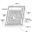
第2実施例は、図2に示す構成である。ここでは、第1実施例のコイル素子の導体コイル3上にも渦巻き状の磁性体コイル2が、直接、接するように形成され、導体コイル3が磁性体コイル2によって上下に挟まれたコイル素子になっている。それに応じて、中心部と周辺部の壁部5も、導体材料部分7が磁性体材料部分6によって上下に挟まれた積層構造になっている。
(Second embodiment)
The second embodiment has the configuration shown in FIG. Here, a coil element in which a spiral magnetic coil 2 is formed so as to be in direct contact with the conductor coil 3 of the coil element of the first embodiment, and the conductor coil 3 is vertically sandwiched between the magnetic coils 2. It has become. Accordingly, the central and
本実施例のコイル素子も、引き出し電極8から通電することによって磁束を発生し、磁束はコイルの中心部に集中するが、コイルから発生した磁束を上下で遮蔽してより中心部に収束させるために、上下の磁性体コイル2で、直接、導体コイル3を挟んで配置した積層コイル4を形成する。磁束を遮蔽する上下の磁性体コイル2の配線材料は鉄−ニッケル合金であり、導体コイル3は銅である。導体コイル3の上下に配置された磁性体コイル2は、コイル両端の引き出し電極8から通電することで発生する磁束をより収束させる機能がある。 The coil element of the present embodiment also generates magnetic flux when energized from the extraction electrode 8, and the magnetic flux is concentrated at the center of the coil, but the magnetic flux generated from the coil is shielded at the top and bottom to converge more on the center. Then, the laminated coil 4 is formed with the upper and lower magnetic coils 2 and the conductor coil 3 interposed therebetween. The wiring material of the upper and lower magnetic coils 2 that shield the magnetic flux is an iron-nickel alloy, and the conductor coil 3 is copper. The magnetic coils 2 arranged above and below the conductor coil 3 have a function of further converging the magnetic flux generated by energizing from the extraction electrodes 8 at both ends of the coil.
また、コイルの中心部に、積層コイル4と電気的な接続の無い磁性体部分6と導体材料部分7からなる壁部5を設ける。これはコイルコアの役割をなし、コイル中心部の磁束をより収束させる。さらに、コイル外周部にも、積層コイル4と電気的な接続の無い磁性体部分6と導体材料部分7からなる壁部5を設ける。これはヨークの機能を有し、磁束がコイル外周に拡がっていくのを抑制する役割をなす。
Moreover, the
次に、本実施例のコイル素子の作製工程の一例を示す。
まず、シリコンの基板表面に絶縁膜としてSiO2が形成してある基板1に、電極層としてスパッタ成膜によってチタンと鉄−ニッケル合金を成膜する。次に、ネガ型エポキシ系ラミネートフィルムを貼り、フォトリソグラフィにより、渦巻状のコイルパターンとコイルパターン中心部および外周部に開口部を形成する。この際、第1実施例と同じフォトマスクを使用した。形成した開口部に鉄−ニッケル合金メッキをし、その上に連続して銅メッキを行い、さらに連続して鉄−ニッケル合金メッキをする。そして、第1実施例と同様に、フォトレジストの除去、電極層のエッチングを行うことによって本実施例のコイルを作製した。両端の取り出し電極8に導通テスターを当てたところ導通が確認できた。
Next, an example of a manufacturing process of the coil element of this embodiment will be described.
First, titanium and an iron-nickel alloy are formed by sputtering as an electrode layer on a substrate 1 in which SiO 2 is formed as an insulating film on the surface of a silicon substrate. Next, a negative epoxy laminate film is applied, and a spiral coil pattern and openings are formed in the coil pattern central part and outer peripheral part by photolithography. At this time, the same photomask as in the first example was used. Iron-nickel alloy plating is performed on the formed opening, copper plating is continuously performed thereon, and iron-nickel alloy plating is further performed continuously. Then, similarly to the first example, the coil of this example was manufactured by removing the photoresist and etching the electrode layer. When a continuity tester was applied to the extraction electrodes 8 at both ends, conduction was confirmed.
(第3実施例)
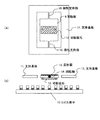
本実施例は本発明のコイル素子を用いた光偏向器に係わる。可動板9が、2つの弾性支持部10により、支持基板11にねじり回転可能に支持されている。可動板9、弾性支持部10、支持基板11は、シリコン基板をエッチング加工することにより一体形成される。可動板19上には反射膜13が形成される。また、可動板9の反射膜13と反対側には可動磁石12が接合されている。可動磁石12の着磁方向は、一対の弾性支持部10の伸長方向に対して直交している。基板11に対向する位置には、本発明のコイル素子15が配置されている。
(Third embodiment)
The present embodiment relates to an optical deflector using the coil element of the present invention. The movable plate 9 is supported on the support substrate 11 by two elastic support portions 10 so as to be torsionally rotated. The movable plate 9, the elastic support portion 10, and the support substrate 11 are integrally formed by etching the silicon substrate. A reflective film 13 is formed on the movable plate 19. Further, a movable magnet 12 is bonded to the movable plate 9 on the side opposite to the reflective film 13. The magnetization direction of the movable magnet 12 is orthogonal to the extending direction of the pair of elastic support portions 10. The coil element 15 of the present invention is disposed at a position facing the substrate 11.
次に、駆動方法を説明する。コイル素子15に電流を流すことで発生する磁場が可動磁石12に作用し、可動板9を一対の弾性支持部10の回りで偏向させる。コイル素子15に電流を流したところ可動部9の駆動が認められ、可動板9は、一対の弾性支持部10で規定される回転軸を中心に偏向角±15°で振れた。本発明のコイル素子15はコイル中心部に効果的に大きな磁場を発生できるため、可動磁石12に対して大きな駆動力を作用させられ、比較的低電圧で駆動できる。 Next, a driving method will be described. A magnetic field generated by passing a current through the coil element 15 acts on the movable magnet 12 to deflect the movable plate 9 around the pair of elastic support portions 10. When a current was passed through the coil element 15, the driving of the movable portion 9 was recognized, and the movable plate 9 was swung with a deflection angle of ± 15 ° around the rotation axis defined by the pair of elastic support portions 10. Since the coil element 15 of the present invention can effectively generate a large magnetic field in the central part of the coil, a large driving force can be applied to the movable magnet 12 and it can be driven at a relatively low voltage.
(第4実施例)
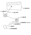
本実施例は、本発明による第3実施例の光偏向器を用いた画像形成装置の例である。図4に本実施例の構成を示す。まず、光源変調駆動部16から出た変調信号17により直接変調光源18の変調を行う。本実施例においては、直接変調光源18として赤色の半導体レーザを用いた。直接変調光源18は、また、赤色、青色、緑色の直接変調可能な光源を用い、これらを混色光学系にて混色して用いてもよい。直接変調光源18で直接変調された出力光19は、光偏向器20の反射面に照射されて一方向に偏向される。さらに、この一方向に偏向された光は別の光偏向器20により反射されて該一方向と直交する方向に偏向され、この反射光は、補正光学系21を通って画像表示体22上に画像として表示される。補正光学系21は、共振走査による画像の歪みを補正する光学系である。本発明の光偏向器は、2つの光偏向器20のうち少なくとも一方に用いられる。
(Fourth embodiment)
This embodiment is an example of an image forming apparatus using the optical deflector of the third embodiment according to the present invention. FIG. 4 shows the configuration of this embodiment. First, the modulation light source 18 is directly modulated by the modulation signal 17 output from the light source modulation drive unit 16. In this embodiment, a red semiconductor laser is used as the direct modulation light source 18. The direct modulation light source 18 may be a red, blue, or green light source that can be directly modulated, and these may be mixed by a color mixing optical system. The output light 19 directly modulated by the direct modulation light source 18 is applied to the reflecting surface of the optical deflector 20 and deflected in one direction. Further, the light deflected in one direction is reflected by another optical deflector 20 and deflected in a direction orthogonal to the one direction, and this reflected light passes through the correction optical system 21 and onto the image display body 22. Displayed as an image. The correction optical system 21 is an optical system that corrects image distortion due to resonance scanning. The optical deflector of the present invention is used for at least one of the two optical deflectors 20.
こうして、本発明の光偏向器20を用いて直接変調された出力光は画像表示体22に画像を表示する。本発明による一方の光偏向器(可動ミラー)20による高速走査は、周波数20kHzの共振駆動往復描画に係わり、その偏向角は±15°で、反射角にすると±30°である。本発明によるこの光偏向器20はコンパクトな構成にできて、その駆動電圧は比較的低くできて、8Vである。この様に、本実施例により、コンパクトな構成を有し、比較的低電圧で駆動でき、偏向角が大きく高精細な画像が得られる画像形成装置を実現することができた。 Thus, the output light directly modulated using the optical deflector 20 of the present invention displays an image on the image display body 22. The high-speed scanning by one optical deflector (movable mirror) 20 according to the present invention is related to resonance-driven reciprocating drawing with a frequency of 20 kHz, the deflection angle is ± 15 °, and the reflection angle is ± 30 °. This optical deflector 20 according to the present invention can be made compact and its drive voltage can be relatively low, 8V. Thus, according to the present embodiment, an image forming apparatus that has a compact configuration, can be driven at a relatively low voltage, and has a large deflection angle and a high-definition image can be realized.
1 基板
2 磁性体コイル
3 導体コイル
4 積層コイル
5 磁性体と導体材料からなる壁部
6 磁性体材料部分
7 導体材料部分
DESCRIPTION OF SYMBOLS 1 Board | substrate 2 Magnetic body coil 3 Conductor coil 4
Claims (9)
The spiral coiled magnetic coil is formed on the multilayer coil so as to be in direct contact, and the conductor coil has a multilayer coil sandwiched between the magnetic coils. The coil element as described.
9. An image forming apparatus comprising: the actuator according to claim 8; and a light source, wherein the light from the light source is deflected by the actuator to form an image on a desired surface.
Priority Applications (1)
| Application Number | Priority Date | Filing Date | Title |
|---|---|---|---|
| JP2004105839A JP2005294445A (en) | 2004-03-31 | 2004-03-31 | Coil element |
Applications Claiming Priority (1)
| Application Number | Priority Date | Filing Date | Title |
|---|---|---|---|
| JP2004105839A JP2005294445A (en) | 2004-03-31 | 2004-03-31 | Coil element |
Publications (1)
| Publication Number | Publication Date |
|---|---|
| JP2005294445A true JP2005294445A (en) | 2005-10-20 |
Family
ID=35327060
Family Applications (1)
| Application Number | Title | Priority Date | Filing Date |
|---|---|---|---|
| JP2004105839A Pending JP2005294445A (en) | 2004-03-31 | 2004-03-31 | Coil element |
Country Status (1)
| Country | Link |
|---|---|
| JP (1) | JP2005294445A (en) |
Cited By (5)
| Publication number | Priority date | Publication date | Assignee | Title |
|---|---|---|---|---|
| WO2013046399A1 (en) * | 2011-09-29 | 2013-04-04 | 古河電気工業株式会社 | Electromagnet wire rod and coil |
| WO2013051102A1 (en) * | 2011-10-04 | 2013-04-11 | 古河電気工業株式会社 | Wire rod for inductor, and inductor |
| WO2015079773A1 (en) * | 2013-11-28 | 2015-06-04 | 株式会社村田製作所 | Electromagnet, camera-lens driving method, and electromagnet manufacturing method |
| JP2021158377A (en) * | 2017-04-13 | 2021-10-07 | 大日本印刷株式会社 | Inductors, inductor manufacturing methods, passive devices and semiconductor devices |
| KR20220092125A (en) | 2020-12-24 | 2022-07-01 | 삼성전기주식회사 | Coil component |
-
2004
- 2004-03-31 JP JP2004105839A patent/JP2005294445A/en active Pending
Cited By (8)
| Publication number | Priority date | Publication date | Assignee | Title |
|---|---|---|---|---|
| WO2013046399A1 (en) * | 2011-09-29 | 2013-04-04 | 古河電気工業株式会社 | Electromagnet wire rod and coil |
| WO2013051102A1 (en) * | 2011-10-04 | 2013-04-11 | 古河電気工業株式会社 | Wire rod for inductor, and inductor |
| WO2015079773A1 (en) * | 2013-11-28 | 2015-06-04 | 株式会社村田製作所 | Electromagnet, camera-lens driving method, and electromagnet manufacturing method |
| US10147529B2 (en) | 2013-11-28 | 2018-12-04 | Murata Manufacturing Co., Ltd. | Electromagnet, camera lens driving device, and production method of electromagnet |
| JP2021158377A (en) * | 2017-04-13 | 2021-10-07 | 大日本印刷株式会社 | Inductors, inductor manufacturing methods, passive devices and semiconductor devices |
| JP7138854B2 (en) | 2017-04-13 | 2022-09-20 | 大日本印刷株式会社 | INDUCTOR, INDUCTOR MANUFACTURING METHOD, PASSIVE DEVICE AND SEMICONDUCTOR DEVICE |
| KR20220092125A (en) | 2020-12-24 | 2022-07-01 | 삼성전기주식회사 | Coil component |
| US12476043B2 (en) | 2020-12-24 | 2025-11-18 | Samsung Electro-Mechanics Co., Ltd. | Coil component |
Similar Documents
| Publication | Publication Date | Title |
|---|---|---|
| US11309114B2 (en) | Stacked body and method of producing stacked body | |
| JP3724405B2 (en) | Common mode choke coil | |
| JP4247518B2 (en) | Small inductor / transformer and manufacturing method thereof | |
| JP6716865B2 (en) | Coil parts | |
| US7417523B2 (en) | Ultra-thin flexible inductor | |
| JP7243569B2 (en) | Inductor components and substrates with built-in inductor components | |
| CN101266868B (en) | Ultra-small electric power conversion device | |
| JP2016225465A (en) | Coil component | |
| JP4434268B2 (en) | Electronic component module | |
| JP6716866B2 (en) | Coil parts | |
| JPH05291063A (en) | Magnetic induction element | |
| CN119049845A (en) | Inductance component | |
| JP6716867B2 (en) | Coil component and manufacturing method thereof | |
| JP2770750B2 (en) | Inductance element | |
| CN112466597A (en) | Inductor component | |
| JP2005223147A (en) | Chip coil | |
| JP2000277354A (en) | Laminated common mode choke coil | |
| JP2005294445A (en) | Coil element | |
| JP6477262B2 (en) | Coil parts | |
| JP2022139098A (en) | Inductor component and electronic component | |
| JP4064049B2 (en) | Manufacturing method of multilayer electronic component | |
| JP2017017141A (en) | Coil component | |
| JP2005175347A (en) | Coil element | |
| JP2022126115A (en) | Laminated coil component | |
| JP2000114046A (en) | Thin film transformer |