JP2005294328A - Method and system for managing early warning of semiconductor manufacturing device - Google Patents
Method and system for managing early warning of semiconductor manufacturing device Download PDFInfo
- Publication number
- JP2005294328A JP2005294328A JP2004103401A JP2004103401A JP2005294328A JP 2005294328 A JP2005294328 A JP 2005294328A JP 2004103401 A JP2004103401 A JP 2004103401A JP 2004103401 A JP2004103401 A JP 2004103401A JP 2005294328 A JP2005294328 A JP 2005294328A
- Authority
- JP
- Japan
- Prior art keywords
- semiconductor manufacturing
- early warning
- manufacturing apparatus
- analysis
- parameters
- Prior art date
- Legal status (The legal status is an assumption and is not a legal conclusion. Google has not performed a legal analysis and makes no representation as to the accuracy of the status listed.)
- Granted
Links
Images
Classifications
-
- Y—GENERAL TAGGING OF NEW TECHNOLOGICAL DEVELOPMENTS; GENERAL TAGGING OF CROSS-SECTIONAL TECHNOLOGIES SPANNING OVER SEVERAL SECTIONS OF THE IPC; TECHNICAL SUBJECTS COVERED BY FORMER USPC CROSS-REFERENCE ART COLLECTIONS [XRACs] AND DIGESTS
- Y02—TECHNOLOGIES OR APPLICATIONS FOR MITIGATION OR ADAPTATION AGAINST CLIMATE CHANGE
- Y02P—CLIMATE CHANGE MITIGATION TECHNOLOGIES IN THE PRODUCTION OR PROCESSING OF GOODS
- Y02P90/00—Enabling technologies with a potential contribution to greenhouse gas [GHG] emissions mitigation
- Y02P90/02—Total factory control, e.g. smart factories, flexible manufacturing systems [FMS] or integrated manufacturing systems [IMS]
-
- Y—GENERAL TAGGING OF NEW TECHNOLOGICAL DEVELOPMENTS; GENERAL TAGGING OF CROSS-SECTIONAL TECHNOLOGIES SPANNING OVER SEVERAL SECTIONS OF THE IPC; TECHNICAL SUBJECTS COVERED BY FORMER USPC CROSS-REFERENCE ART COLLECTIONS [XRACs] AND DIGESTS
- Y02—TECHNOLOGIES OR APPLICATIONS FOR MITIGATION OR ADAPTATION AGAINST CLIMATE CHANGE
- Y02P—CLIMATE CHANGE MITIGATION TECHNOLOGIES IN THE PRODUCTION OR PROCESSING OF GOODS
- Y02P90/00—Enabling technologies with a potential contribution to greenhouse gas [GHG] emissions mitigation
- Y02P90/80—Management or planning
Landscapes
- General Factory Administration (AREA)
- Testing Or Measuring Of Semiconductors Or The Like (AREA)
Abstract
Description
この発明は半導体製造装置を管理する方法及びシステムに関し、特に半導体製造装置の早期警報管理方法及びその関連システムに関する。 The present invention relates to a method and system for managing a semiconductor manufacturing apparatus, and more particularly to an early warning management method for a semiconductor manufacturing apparatus and a related system.
半導体製造装置が作動する前に、その機能と動作パラメーターを調整するため、早期警報管理を行わなければならない。従来の技術によれば、半導体製造装置の早期警報管理は経験のある技師によって行われる。半導体製作工程におけるデータを測定して分析し、その分析結果によって早期警報管理を行う。しかし、この分析結果は人力による判断と評価に頼るものであり、それで半導体製造装置を即時に調整することは不可能である。なお、従来の分析は、半導体製造装置の機能、製作工程のデータ測定など個別の分析にとどまり、早期警報管理のための統合的なデータは欠如である。更に、従来の分析は技師の経験に依存するもので、人事異動があればその経験は流失しかねない。 Prior to the operation of semiconductor manufacturing equipment, early warning management must be performed to adjust its functions and operating parameters. According to the prior art, early warning management of semiconductor manufacturing equipment is performed by experienced engineers. Data in the semiconductor manufacturing process is measured and analyzed, and early warning management is performed based on the analysis result. However, this analysis result relies on human judgment and evaluation, and it is impossible to immediately adjust the semiconductor manufacturing apparatus. The conventional analysis is limited to individual analysis such as the function of the semiconductor manufacturing apparatus and measurement of manufacturing process data, and there is a lack of integrated data for early warning management. Furthermore, conventional analysis relies on the experience of engineers, and if there are personnel changes, that experience can be lost.
この発明は前述の問題を解決するための半導体製造装置の早期警報管理方法及びその関連システムを提供することを課題とする。 An object of the present invention is to provide an early warning management method for a semiconductor manufacturing apparatus and related systems for solving the above-mentioned problems.
この発明は1台以上の半導体製造装置に対する早期警報管理方法を提供する。各半導体製造装置は1個以上のプロセスパラメーターによって複数の半導体製品に対して工程を行う。当方法は、各半導体製造装置のプロセスパラメーターを記録し、各半導体製造装置が製作工程を行うとともに、工程の状態を装置パラメーターとして記録し、各半導体製造装置が製作工程を終了した後、工程終了後の製品品質を評価してテストパラメーターを記録し、各半導体製造装置に対応するプロセスパラメーターと、装置パラメーターと、製品の品質を統計分析するなどのステップを含む。 The present invention provides an early warning management method for one or more semiconductor manufacturing apparatuses. Each semiconductor manufacturing apparatus performs a process on a plurality of semiconductor products according to one or more process parameters. This method records the process parameters of each semiconductor manufacturing device, each semiconductor manufacturing device performs the manufacturing process, records the state of the process as a device parameter, and after each semiconductor manufacturing device finishes the manufacturing process, the process ends. It includes steps such as statistically analyzing process parameters corresponding to each semiconductor manufacturing equipment, equipment parameters, and product quality by evaluating the quality of the subsequent product and recording test parameters.
この発明は更に1台以上の半導体製造装置に対する早期警報管理システムを提供する。各半導体製造装置は1個以上のプロセスパラメーターによって複数の半導体製品に対して工程を行う。当システムは、各半導体製造装置のプロセスパラメーターを記録する工程インターフェイスモジュールと、各半導体製造装置が製作工程を行うとともに、工程の状態を装置パラメーターとして記録する装置インターフェイスモジュールと、各半導体製造装置が製作工程を終了した後、工程終了後の製品品質とテストパラメーターを記録する品質モニターモジュールと、各半導体製造装置に対応するプロセスパラメーターと、装置パラメーターと、製品の品質を統計分析する分析モジュールとを含む。 The present invention further provides an early warning management system for one or more semiconductor manufacturing apparatuses. Each semiconductor manufacturing apparatus performs a process on a plurality of semiconductor products according to one or more process parameters. This system is a process interface module that records the process parameters of each semiconductor manufacturing device, a device interface module that records the state of the process as a device parameter, and a semiconductor interface that manufactures each semiconductor manufacturing device. Includes a quality monitor module that records the product quality and test parameters after completion of the process, a process parameter corresponding to each semiconductor manufacturing equipment, equipment parameters, and an analysis module that statistically analyzes the product quality .
この発明による半導体製造装置の早期警報管理は、新規の半導体製造装置が働き始めてから統計と分析を行うことによって、安定性調整、工程条件調整、機差調整などを可能にさせる。 The early warning management of a semiconductor manufacturing apparatus according to the present invention enables stability adjustment, process condition adjustment, machine difference adjustment, etc. by performing statistics and analysis after a new semiconductor manufacturing apparatus starts to work.
かかる方法及び装置の特徴を詳述するために、具体的な実施例を挙げ、図示を参照にして以下に説明する。 In order to detail the features of such a method and apparatus, a specific example is given and described below with reference to the drawings.
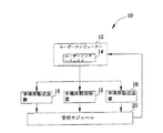
図1を参照する。図1はこの発明による半導体製造装置の早期警報管理システム10を表す説明図である。早期警報管理システム10は、ユーザーインターフェイス14を有するユーザーコンピューター12(例えばサーバー)と、複数の半導体製造装置18と、管理モジュール20とを含む。ユーザーコンピューター12は半導体製造装置18と接続される。使用者はユーザーインターフェイス14で半導体製造装置18の早期警報管理を行う。半導体製造装置18はいずれも管理モジュール20と接続され、管理モジュール20はユーザーコンピューター12と接続される。半導体製作工程において、管理モジュール20は製作工程におけるパラメーターとテスト結果を記録して分析してから、分析結果をネットワークを通して遠隔のユーザーコンピューター12に送信し、図表でユーザーインターフェイス14を通して表示する。のみならず、管理モジュール20は分析結果をユーザーインターフェイス14を通して使用者(例えば保守担当の技師)が早期警報管理の過程をモニターできるようなモニターフィードバックインターフェイスを形成する。
Please refer to FIG. FIG. 1 is an explanatory diagram showing an early
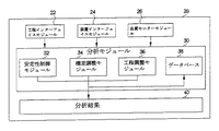
図2を参照する。図2は図1における管理モジュール20のブロック図である。管理モジュール20は工程インターフェイスモジュール22と、装置インターフェイスモジュール24と、品質モニターモジュール26と、分析モジュール30とからなる。図1における半導体製造装置18がプロセスパラメーターによって工程を開始すれば、工程インターフェイスモジュール22は半導体製造装置18に対応するプロセスパラメーターを記録する。同時に装置インターフェイスモジュール24は半導体製造装置18による工程の状態を装置パラメーターとして記録する。半導体製造装置18による工程が終了すれば、品質モニターモジュール26は製品の品質とテストパラメーターを記録する。
Please refer to FIG. FIG. 2 is a block diagram of the
分析モジュール30は工程インターフェイスモジュール22と、装置インターフェイスモジュール24と、品質モニターモジュール26と接続され、各半導体製造装置18のプロセスパラメーターと、装置パラメーターと、製品の品質とを分析する。分析モジュール30は安定性制御モジュール32と、機差調整モジュール34と、工程調整モジュール36と、データベース38とを含む。各モジュールはT検定、一元配置分散分析(ANOVA)、二元配置分散分析または箱ひげ図などの方法で分析し、分析結果40を図1におけるユーザーコンピューター12に送信する。データベース38は関連の装置パラメーターと、プロセスパラメーターと、分析結果を保存する。安定性制御モジュール32は半導体製造装置18の安定性を制御し、機差調整モジュール34は半導体製造装置18間の機差を調整し、工程調整モジュール36は半導体製作工程の標準処理手順(SOP)を調整するものである。分析モジュール30にある各モジュールの働きに基づいて、プロセスパラメーターと、装置パラメーターと、製品の品質によって早期警報管理を行う。例えば、半導体製造装置を一定の期間に使用すれば、製品の品質によって製造装置の働きに異常があるかどうかを判断できる。なお、早期警報管理を行えば、プロセスパラメーターと、装置パラメーターと、製品の品質によってメーカーが異なる製造装置の性能差(いわゆる機差)を判断できる。
The analysis module 30 is connected to the
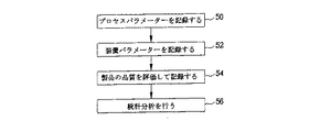
図3を参照する。図3はこの発明による半導体製造装置の早期警報管理方法を表すフローチャートである。その内容は以下の通りである。
ステップ50: 半導体製造装置18はプロセスパラメーターによって製作工程を開始して、工程インターフェイスモジュール22は半導体製造装置18の各プロセスパラメーターを記録する。
ステップ52: 半導体製造装置18による工程が行われるとともに、装置インターフェイスモジュール24は工程の実行状態を装置パラメーターとして記録する。
ステップ54: 製作工程が終われば、品質モニターモジュール26は製品の品質とテストパラメーターを記録する。
ステップ56: 分析モジュール30はT検定、一元配置分散分析(ANOVA)、二元配置分散分析または箱ひげ図などの方法で前述のデータを分析し、分析結果40を図1におけるユーザーコンピューター12に送信する。
Please refer to FIG. FIG. 3 is a flowchart showing an early warning management method for a semiconductor manufacturing apparatus according to the present invention. The contents are as follows.
Step 50: The
Step 52: While the process by the
Step 54: Once the production process is complete, the quality monitor module 26 records the product quality and test parameters.
Step 56: The analysis module 30 analyzes the above-described data by a method such as T test, one-way analysis of variance (ANOVA), two-way analysis of variance or boxplot, and sends the
以上の半導体製造装置の予防保守は、ウエハー加工におけるテスト結果を統計分析し、ロット、ウエハー、装置によって製品別でウエハー加工データと統計データを図表で示す。ウエハー加工データは加工ステップ、ロット、チャンバー、加工時間などを含み、統計データはウエハーテスト、サンプルテスト、チップパッケージ後の最終テスト、各ウエハーまたは各加工モジュールの測定データと歩留まりなどを含む。これらのデータは平均値、標準偏差、T検定などの方法で図表で示され、データによって半導体製造装置の早期警報管理は行われる。 In the preventive maintenance of the semiconductor manufacturing apparatus described above, the test results in the wafer processing are statistically analyzed, and the wafer processing data and statistical data are shown in a chart by product by lot, wafer, and apparatus. Wafer processing data includes processing steps, lots, chambers, processing times, etc., and statistical data includes wafer test, sample test, final test after chip packaging, measurement data and yield of each wafer or each processing module, and the like. These data are shown in a chart by a method such as an average value, standard deviation, T test, etc., and early warning management of the semiconductor manufacturing apparatus is performed by the data.
以上はこの発明に好ましい実施例であって、この発明の実施の範囲を限定するものではない。よって、当業者のなし得る修正、もしくは変更であって、この発明の精神の下においてなされ、この発明に対して均等の効果を有するものは、いずれもこの発明の特許請求の範囲に属するものとする。 The above is a preferred embodiment of the present invention and does not limit the scope of the present invention. Therefore, any modifications or changes that can be made by those skilled in the art, which are made within the spirit of the present invention and have an equivalent effect on the present invention, shall belong to the scope of the claims of the present invention. To do.
この発明による半導体製造装置の早期警報管理は、新規の半導体製造装置が働き始めてから統計と分析を行うことによって、安定性調整、工程条件調整、機差調整などを可能にさせる。 The early warning management of a semiconductor manufacturing apparatus according to the present invention enables stability adjustment, process condition adjustment, machine difference adjustment, etc. by performing statistics and analysis after a new semiconductor manufacturing apparatus starts to work.
10 早期警報管理システム
12 ユーザーコンピューター
14 ユーザーインターフェイス
18 半導体製造装置
20 管理モジュール
22 工程インターフェイスモジュール
24 装置インターフェイスモジュール
26 品質モニターモジュール
30 分析モジュール
32 安定性制御モジュール
34 機差調整モジュール
36 工程調整モジュール
38 データベース
40 分析結果
DESCRIPTION OF
Claims (14)
各半導体製造装置のプロセスパラメーターを記録し、
各半導体製造装置が製作工程を行うとともに、工程の状態を装置パラメーターとして記録し、
各半導体製造装置が製作工程を終了した後、工程終了後の製品品質を評価してテストパラメーターを記録し、
各半導体製造装置に対応するプロセスパラメーターと、装置パラメーターと、製品の品質を統計分析するなどのステップを含むことを特徴とする半導体製造装置の早期警報管理方法。 In the early warning management method for one or more semiconductor manufacturing apparatuses, each semiconductor manufacturing apparatus performs a process on a plurality of semiconductor products according to one or more process parameters.
Record the process parameters of each semiconductor manufacturing equipment,
While each semiconductor manufacturing device performs the manufacturing process, the state of the process is recorded as a device parameter,
After each semiconductor manufacturing device finishes the manufacturing process, evaluate the product quality after the end of the process and record the test parameters,
An early warning management method for a semiconductor manufacturing apparatus, comprising the steps of statistically analyzing process parameters corresponding to each semiconductor manufacturing apparatus, apparatus parameters, and product quality.
型番が同じか異なった2台以上の半導体製造装置による製品品質に基づいて、同じ製作工程における半導体製造装置間の機差を分析するステップを含むことを特徴とする請求項1記載の半導体製造装置の早期警報管理方法。 The statistical analysis further includes
2. The semiconductor manufacturing apparatus according to claim 1, further comprising a step of analyzing a machine difference between semiconductor manufacturing apparatuses in the same manufacturing process based on product quality of two or more semiconductor manufacturing apparatuses having the same or different model numbers. Early warning management method.
各半導体製造装置のプロセスパラメーターと、装置パラメーターと、製品の品質と、分析結果をデータベースに記録するステップを含むことを特徴とする請求項1記載の半導体製造装置の早期警報管理方法。 The method further comprises:
The early warning management method for a semiconductor manufacturing apparatus according to claim 1, further comprising a step of recording a process parameter of each semiconductor manufacturing apparatus, apparatus parameters, product quality, and analysis result in a database.
統計分析を行った後、モニターフィードバックを行って統計分析の結果をネットワークまたはマンマシンインターフェイス(MMI)で使用者に示すことを特徴とする請求項1記載の半導体製造装置の早期警報管理方法。 The method further comprises:
2. The early warning management method for a semiconductor manufacturing apparatus according to claim 1, wherein after performing the statistical analysis, monitor feedback is performed to show the result of the statistical analysis to the user through a network or a man-machine interface (MMI).
各半導体製造装置のプロセスパラメーターを記録する工程インターフェイスモジュールと、
各半導体製造装置が製作工程を行うとともに、工程の状態を装置パラメーターとして記録する装置インターフェイスモジュールと、
各半導体製造装置が製作工程を終了した後、工程終了後の製品品質とテストパラメーターを記録する品質モニターモジュールと、
各半導体製造装置に対応するプロセスパラメーターと、装置パラメーターと、製品の品質を統計分析する分析モジュールとを含むことを特徴とする半導体製造装置の早期警報管理システム。 In an early warning management system for one or more semiconductor manufacturing apparatuses, each semiconductor manufacturing apparatus performs a process on a plurality of semiconductor products according to one or more process parameters.
A process interface module for recording process parameters of each semiconductor manufacturing apparatus;
Each semiconductor manufacturing apparatus performs a manufacturing process, and an apparatus interface module that records the state of the process as an apparatus parameter;
After each semiconductor manufacturing device finishes the manufacturing process, a quality monitor module that records product quality and test parameters after the process ends,
An early warning management system for semiconductor manufacturing equipment, comprising: process parameters corresponding to each semiconductor manufacturing equipment; equipment parameters; and an analysis module for statistically analyzing product quality.
統計分析を行った後、統計分析の結果をネットワークまたはマンマシンインターフェイス(MMI)で使用者に示すモニターフィードバックインターフェイスを含むことを特徴とする請求項8記載の半導体製造装置の早期警報管理システム。 The system further includes:
9. The early warning management system for a semiconductor manufacturing apparatus according to claim 8, further comprising a monitor feedback interface for showing a result of the statistical analysis to a user through a network or a man-machine interface (MMI) after performing the statistical analysis.
Priority Applications (1)
| Application Number | Priority Date | Filing Date | Title |
|---|---|---|---|
| JP2004103401A JP4177780B2 (en) | 2004-03-31 | 2004-03-31 | Early warning management method and system for semiconductor manufacturing equipment |
Applications Claiming Priority (1)
| Application Number | Priority Date | Filing Date | Title |
|---|---|---|---|
| JP2004103401A JP4177780B2 (en) | 2004-03-31 | 2004-03-31 | Early warning management method and system for semiconductor manufacturing equipment |
Publications (2)
| Publication Number | Publication Date |
|---|---|
| JP2005294328A true JP2005294328A (en) | 2005-10-20 |
| JP4177780B2 JP4177780B2 (en) | 2008-11-05 |
Family
ID=35326966
Family Applications (1)
| Application Number | Title | Priority Date | Filing Date |
|---|---|---|---|
| JP2004103401A Expired - Lifetime JP4177780B2 (en) | 2004-03-31 | 2004-03-31 | Early warning management method and system for semiconductor manufacturing equipment |
Country Status (1)
| Country | Link |
|---|---|
| JP (1) | JP4177780B2 (en) |
Cited By (4)
| Publication number | Priority date | Publication date | Assignee | Title |
|---|---|---|---|---|
| JP2010507253A (en) * | 2006-10-16 | 2010-03-04 | バリアン・セミコンダクター・エクイップメント・アソシエイツ・インコーポレイテッド | Technology to match performance between ion implantation devices using in situ mask |
| US10671056B2 (en) | 2017-07-20 | 2020-06-02 | Kokusai Electric Corporation | Substrate processing system |
| CN116802579A (en) * | 2021-01-29 | 2023-09-22 | 应用材料公司 | Process anomaly identification using measurement violation analysis |
| CN118016572A (en) * | 2024-04-08 | 2024-05-10 | 南通优睿半导体有限公司 | Semiconductor Equipment Alarm Management System |
-
2004
- 2004-03-31 JP JP2004103401A patent/JP4177780B2/en not_active Expired - Lifetime
Cited By (5)
| Publication number | Priority date | Publication date | Assignee | Title |
|---|---|---|---|---|
| JP2010507253A (en) * | 2006-10-16 | 2010-03-04 | バリアン・セミコンダクター・エクイップメント・アソシエイツ・インコーポレイテッド | Technology to match performance between ion implantation devices using in situ mask |
| US10671056B2 (en) | 2017-07-20 | 2020-06-02 | Kokusai Electric Corporation | Substrate processing system |
| US11726456B2 (en) | 2017-07-20 | 2023-08-15 | Kokusai Electric Corporation | Substrate processing system |
| CN116802579A (en) * | 2021-01-29 | 2023-09-22 | 应用材料公司 | Process anomaly identification using measurement violation analysis |
| CN118016572A (en) * | 2024-04-08 | 2024-05-10 | 南通优睿半导体有限公司 | Semiconductor Equipment Alarm Management System |
Also Published As
| Publication number | Publication date |
|---|---|
| JP4177780B2 (en) | 2008-11-05 |
Similar Documents
| Publication | Publication Date | Title |
|---|---|---|
| US8046193B2 (en) | Determining process condition in substrate processing module | |
| US6825050B2 (en) | Integrated stepwise statistical process control in a plasma processing system | |
| JP4615222B2 (en) | Correlation between line end data mining and process tool data mining | |
| US20190198405A1 (en) | Statistical framework for tool chamber matching in semiconductor manufacturing processes | |
| CN105702595A (en) | Wafer yield judging method and wafer qualification test multivariable detection method | |
| WO2019016892A1 (en) | Quality analysis device and quality analysis method | |
| US20060189009A1 (en) | Apparatus for controlling semiconductor manufacturing process | |
| JP4177780B2 (en) | Early warning management method and system for semiconductor manufacturing equipment | |
| CN102478842B (en) | A method and device for optimizing a measurement process | |
| JP2011054804A (en) | Method and system for management of semiconductor manufacturing device | |
| US20100017010A1 (en) | Monitoring a process sector in a production facility | |
| JP2009076772A (en) | Process monitoring method | |
| Wu | Modified processes capability assessment with dynamic mean shift | |
| US6999897B2 (en) | Method and related system for semiconductor equipment early warning management | |
| JP4063787B2 (en) | Method and system for managing preventive maintenance of semiconductor manufacturing equipment | |
| KR20230061068A (en) | System and method for matching and analyzing real-time process data of semiconductor equipment | |
| US6950783B1 (en) | Method and related system for semiconductor equipment prevention maintenance management | |
| US7533313B1 (en) | Method and apparatus for identifying outlier data | |
| CN115220409A (en) | Machine bench test operation method and system | |
| KR19990001946A (en) | Semiconductor process management system and process control method | |
| US6766258B1 (en) | Method and apparatus for dynamically enabling trace data collection | |
| CN1670905A (en) | Method and related system for initial flow management of semiconductor equipment | |
| JP2005142384A (en) | Inspection data analysis program | |
| KR20090068600A (en) | Automated Information Analysis Method in Semiconductor Process | |
| CN101174149A (en) | Methodology for establishing control specification boundaries |
Legal Events
| Date | Code | Title | Description |
|---|---|---|---|
| A131 | Notification of reasons for refusal |
Free format text: JAPANESE INTERMEDIATE CODE: A131 Effective date: 20070731 |
|
| A521 | Request for written amendment filed |
Free format text: JAPANESE INTERMEDIATE CODE: A523 Effective date: 20071022 |
|
| A131 | Notification of reasons for refusal |
Free format text: JAPANESE INTERMEDIATE CODE: A131 Effective date: 20071204 |
|
| A521 | Request for written amendment filed |
Free format text: JAPANESE INTERMEDIATE CODE: A523 Effective date: 20080226 |
|
| A02 | Decision of refusal |
Free format text: JAPANESE INTERMEDIATE CODE: A02 Effective date: 20080401 |
|
| A521 | Request for written amendment filed |
Free format text: JAPANESE INTERMEDIATE CODE: A523 Effective date: 20080522 |
|
| A911 | Transfer to examiner for re-examination before appeal (zenchi) |
Free format text: JAPANESE INTERMEDIATE CODE: A911 Effective date: 20080701 |
|
| TRDD | Decision of grant or rejection written | ||
| A01 | Written decision to grant a patent or to grant a registration (utility model) |
Free format text: JAPANESE INTERMEDIATE CODE: A01 Effective date: 20080729 |
|
| A01 | Written decision to grant a patent or to grant a registration (utility model) |
Free format text: JAPANESE INTERMEDIATE CODE: A01 |
|
| A61 | First payment of annual fees (during grant procedure) |
Free format text: JAPANESE INTERMEDIATE CODE: A61 Effective date: 20080822 |
|
| FPAY | Renewal fee payment (event date is renewal date of database) |
Free format text: PAYMENT UNTIL: 20110829 Year of fee payment: 3 |
|
| R150 | Certificate of patent or registration of utility model |
Ref document number: 4177780 Country of ref document: JP Free format text: JAPANESE INTERMEDIATE CODE: R150 Free format text: JAPANESE INTERMEDIATE CODE: R150 |
|
| FPAY | Renewal fee payment (event date is renewal date of database) |
Free format text: PAYMENT UNTIL: 20120829 Year of fee payment: 4 |
|
| R250 | Receipt of annual fees |
Free format text: JAPANESE INTERMEDIATE CODE: R250 |
|
| FPAY | Renewal fee payment (event date is renewal date of database) |
Free format text: PAYMENT UNTIL: 20120829 Year of fee payment: 4 |
|
| S531 | Written request for registration of change of domicile |
Free format text: JAPANESE INTERMEDIATE CODE: R313531 |
|
| S533 | Written request for registration of change of name |
Free format text: JAPANESE INTERMEDIATE CODE: R313533 |
|
| FPAY | Renewal fee payment (event date is renewal date of database) |
Free format text: PAYMENT UNTIL: 20120829 Year of fee payment: 4 |
|
| R350 | Written notification of registration of transfer |
Free format text: JAPANESE INTERMEDIATE CODE: R350 |
|
| FPAY | Renewal fee payment (event date is renewal date of database) |
Free format text: PAYMENT UNTIL: 20130829 Year of fee payment: 5 |
|
| R250 | Receipt of annual fees |
Free format text: JAPANESE INTERMEDIATE CODE: R250 |
|
| R250 | Receipt of annual fees |
Free format text: JAPANESE INTERMEDIATE CODE: R250 |
|
| R250 | Receipt of annual fees |
Free format text: JAPANESE INTERMEDIATE CODE: R250 |
|
| R250 | Receipt of annual fees |
Free format text: JAPANESE INTERMEDIATE CODE: R250 |
|
| R250 | Receipt of annual fees |
Free format text: JAPANESE INTERMEDIATE CODE: R250 |
|
| R250 | Receipt of annual fees |
Free format text: JAPANESE INTERMEDIATE CODE: R250 |
|
| R250 | Receipt of annual fees |
Free format text: JAPANESE INTERMEDIATE CODE: R250 |
|
| S111 | Request for change of ownership or part of ownership |
Free format text: JAPANESE INTERMEDIATE CODE: R313113 |
|
| R350 | Written notification of registration of transfer |
Free format text: JAPANESE INTERMEDIATE CODE: R350 |
|
| R250 | Receipt of annual fees |
Free format text: JAPANESE INTERMEDIATE CODE: R250 |
|
| R250 | Receipt of annual fees |
Free format text: JAPANESE INTERMEDIATE CODE: R250 |
|
| R250 | Receipt of annual fees |
Free format text: JAPANESE INTERMEDIATE CODE: R250 |
|
| R250 | Receipt of annual fees |
Free format text: JAPANESE INTERMEDIATE CODE: R250 |
|
| R250 | Receipt of annual fees |
Free format text: JAPANESE INTERMEDIATE CODE: R250 |
|
| EXPY | Cancellation because of completion of term |