JP2005294320A - Semiconductor device and manufacturing method thereof - Google Patents
Semiconductor device and manufacturing method thereof Download PDFInfo
- Publication number
- JP2005294320A JP2005294320A JP2004103218A JP2004103218A JP2005294320A JP 2005294320 A JP2005294320 A JP 2005294320A JP 2004103218 A JP2004103218 A JP 2004103218A JP 2004103218 A JP2004103218 A JP 2004103218A JP 2005294320 A JP2005294320 A JP 2005294320A
- Authority
- JP
- Japan
- Prior art keywords
- solder resist
- semiconductor device
- resist film
- substrate
- film
- Prior art date
- Legal status (The legal status is an assumption and is not a legal conclusion. Google has not performed a legal analysis and makes no representation as to the accuracy of the status listed.)
- Pending
Links
Images


Classifications
-
- H—ELECTRICITY
- H10—SEMICONDUCTOR DEVICES; ELECTRIC SOLID-STATE DEVICES NOT OTHERWISE PROVIDED FOR
- H10W—GENERIC PACKAGES, INTERCONNECTIONS, CONNECTORS OR OTHER CONSTRUCTIONAL DETAILS OF DEVICES COVERED BY CLASS H10
- H10W20/00—Interconnections in chips, wafers or substrates
- H10W20/01—Manufacture or treatment
- H10W20/021—Manufacture or treatment of interconnections within wafers or substrates
- H10W20/023—Manufacture or treatment of interconnections within wafers or substrates the interconnections being through-semiconductor vias
- H10W20/0242—Manufacture or treatment of interconnections within wafers or substrates the interconnections being through-semiconductor vias comprising etching via holes from the back sides of the chips, wafers or substrates
-
- H—ELECTRICITY
- H10—SEMICONDUCTOR DEVICES; ELECTRIC SOLID-STATE DEVICES NOT OTHERWISE PROVIDED FOR
- H10W—GENERIC PACKAGES, INTERCONNECTIONS, CONNECTORS OR OTHER CONSTRUCTIONAL DETAILS OF DEVICES COVERED BY CLASS H10
- H10W20/00—Interconnections in chips, wafers or substrates
- H10W20/01—Manufacture or treatment
- H10W20/021—Manufacture or treatment of interconnections within wafers or substrates
- H10W20/023—Manufacture or treatment of interconnections within wafers or substrates the interconnections being through-semiconductor vias
- H10W20/0234—Manufacture or treatment of interconnections within wafers or substrates the interconnections being through-semiconductor vias comprising etching via holes that stop on pads or on electrodes
-
- H—ELECTRICITY
- H10—SEMICONDUCTOR DEVICES; ELECTRIC SOLID-STATE DEVICES NOT OTHERWISE PROVIDED FOR
- H10W—GENERIC PACKAGES, INTERCONNECTIONS, CONNECTORS OR OTHER CONSTRUCTIONAL DETAILS OF DEVICES COVERED BY CLASS H10
- H10W20/00—Interconnections in chips, wafers or substrates
- H10W20/20—Interconnections within wafers or substrates, e.g. through-silicon vias [TSV]
- H10W20/211—Through-semiconductor vias, e.g. TSVs
- H10W20/216—Through-semiconductor vias, e.g. TSVs characterised by dielectric material at least partially filling the via holes, e.g. covering the through-semiconductor vias in the via holes
-
- H—ELECTRICITY
- H10—SEMICONDUCTOR DEVICES; ELECTRIC SOLID-STATE DEVICES NOT OTHERWISE PROVIDED FOR
- H10W—GENERIC PACKAGES, INTERCONNECTIONS, CONNECTORS OR OTHER CONSTRUCTIONAL DETAILS OF DEVICES COVERED BY CLASS H10
- H10W72/00—Interconnections or connectors in packages
- H10W72/20—Bump connectors, e.g. solder bumps or copper pillars; Dummy bumps; Thermal bumps
Landscapes
- Internal Circuitry In Semiconductor Integrated Circuit Devices (AREA)
- Formation Of Insulating Films (AREA)
Abstract
【課題】信頼性および製造安定性に優れる半導体装置を提供する。
【解決手段】一方の面と他方の面とに開口する接続孔を有する半導体基板102と、半導体基板102の一方の面に設けられている半田ボール116と、半導体基板102の他方の面に設けられている電極106と、少なくとも一部が半導体基板102の接続孔内の一部に設けられており、半田ボール116および電極106と接続する再配線110と、少なくとも一部が半導体基板102の接続孔内の一部および半導体基板102の一方の面に設けられているラミネートタイプのフォトソルダーレジスト膜114と、を備え、ラミネートタイプのフォトソルダーレジスト膜114は、カルド型ポリマーを含有する半導体装置100を提供する。
【選択図】図1
A semiconductor device having excellent reliability and manufacturing stability is provided.
A semiconductor substrate having a connection hole opened on one surface and the other surface, a solder ball provided on one surface of the semiconductor substrate, and provided on the other surface of the semiconductor substrate. The electrode 106 is provided at least partially in the connection hole of the semiconductor substrate 102, the rewiring 110 is connected to the solder ball 116 and the electrode 106, and at least a part is connected to the semiconductor substrate 102. A laminate type photo solder resist film 114 provided on a part of the hole and on one surface of the semiconductor substrate 102, and the laminate type photo solder resist film 114 includes a cardo type polymer. I will provide a.
[Selection] Figure 1
Description
本発明は、半導体装置およびその製造方法に関する。 The present invention relates to a semiconductor device and a manufacturing method thereof.
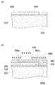
近年、半導体素子の小型化の実現を目的として、半導体チップの小型化だけでなく、半導体パッケージの小型化についても急激に技術が進んできている。その中でも、ウェハーレベルCSPが特に注目され、開発・量産が開始されてきている。ウェハーレベルCSP技術とは、半導体装置のパッケージサイズを半導体チップとほぼ同じ寸法にする目的で、全ての組立工程をウェハー状態で行う技術である。 In recent years, for the purpose of realizing miniaturization of semiconductor elements, not only the miniaturization of a semiconductor chip but also the miniaturization of a semiconductor package has rapidly progressed. Among them, the wafer level CSP attracts special attention, and development / mass production has started. The wafer level CSP technique is a technique for performing all assembly processes in a wafer state for the purpose of making the package size of a semiconductor device substantially the same as that of a semiconductor chip.
CSPのタイプにはさまざまな形態があるが、この種の技術として、特許文献1記載のものがある。同文献に記載された半導体装置の製造方法を示した工程断面図を図8および図9に示す。この半導体装置を製造するには、まず、図8(a)に示すように、半導体チップ832上に電極836、絶縁シート838、金属層840などが設けられた構造を従来公知の技術により製造する。
There are various types of CSP types, and this type of technology is disclosed in Patent Document 1. FIG. 8 and FIG. 9 show process cross-sectional views illustrating the method for manufacturing the semiconductor device described in the document. To manufacture this semiconductor device, first, as shown in FIG. 8A, a structure in which an
次いで、図8(b)に示すように、絶縁シート838および金属層840上に絶縁皮膜842をスピンコート形成法により形成する。この絶縁皮膜は、フォトソルダーレジスト膜であってもよい。この場合、フォトマスクを用いて絶縁皮膜842を一部露光・現像させる。
Next, as shown in FIG. 8B, an
ここで、特に重要な点は、金属層840からなる再配線形成後に、フォトソルダーレジスト(以下、適宜フォトソルダーレジスト膜と略記する)などの絶縁皮膜842をスピンコート形成法により被覆し、金属層840からなる再配線パターンが損傷されないようにしていることである。
Here, a particularly important point is that after the rewiring formed of the
続いて、図9(c)に示すように、一部露光・現像された絶縁皮膜842の露光・現像していない領域を除去して、透孔844を形成する。そして、図9(d)に示すように、透孔844中に外部接続端子846を形成して、外部端子接合部843と接続させる。
Subsequently, as shown in FIG. 9C, a part of the
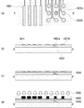
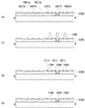
別の従来例として、たとえば、ドライフィルム型の感光性フォトソルダーレジスト膜をラミネートしてコーティングする技術が知られている。この種の技術として、特許文献2記載のものがある。同文献に記載された半導体装置の製造方法を示した工程平面図および工程断面図を図10および図11に示す。 As another conventional example, for example, a technique of laminating and coating a dry film type photosensitive photo solder resist film is known. There exists a thing of patent document 2 as this kind of technique. A process plan view and a process cross-sectional view showing a method of manufacturing a semiconductor device described in the document are shown in FIGS.
この半導体装置を製造するには、まず、図10(a)に示す工程平面図および図10(b)に示す工程平面図のように、半導体基板上に表面実装部品パッド1001、CSPパッド1002a、1002bなどを形成する。
To manufacture this semiconductor device, first, as shown in the process plan view shown in FIG. 10A and the process plan view shown in FIG. 10B, a surface
次いで、図10(c)に示すように、表面実装部品パッド1001、CSPパッド1002a、1002bなどを覆うドライフィルム型のソルダーレジスト1004をラミネートする。
Next, as shown in FIG. 10C, a dry film type solder resist 1004 covering the surface
続いて、図10(d)に示すように、ソルダーレジスト1004上にフォトマスク1005を設け、紫外線1006を照射して、ソルダーレジスト1004を一部露光・現像させる。
Subsequently, as shown in FIG. 10D, a
そして、図11(e)に示すように、一部露光・現像されたソルダーレジスト1004の露光・現像していない領域を除去して、ソルダーレジスト開口部1007a、1007bを形成する。
Then, as shown in FIG. 11E, the part of the solder resist 1004 that has been partially exposed and developed is not exposed and developed to form
次いで、図11(f)に示すように、ソルダーレジスト開口部1007a、1007bの周辺部に炭酸ガスレーザ1008を照射して、ソルダーレジスト1004の残渣も同時に除去する。
Next, as shown in FIG. 11 (f), the
このとき、図11(g)に示すように、ソルダーレジスト開口部1009の周縁部にはソルダーレジストスカム1010が残ることになる。このソルダーレジストスカム1010をエッチング除去することにより、図11(h)に示したような構造を得る。
しかしながら、上記文献記載の従来技術は、以下の点で改善の余地を有していた。 However, the prior art described in the above literature has room for improvement in the following points.
第一に、上記の特許文献1に示した、スピンコート法により形成されたフォトソルダーレジスト膜を用いた半導体装置は、フォトソルダーレジスト膜の耐熱性や機械的強度などが充分ではない場合があった。そのため、半導体装置の信頼性の向上の点でさらなる改善の余地があった。 First, the semiconductor device using the photo solder resist film formed by the spin coating method shown in Patent Document 1 described above may not have sufficient heat resistance, mechanical strength, and the like. It was. Therefore, there is room for further improvement in terms of improving the reliability of the semiconductor device.
ここで、本発明者らは、3次元実装を実現するために、シリコン基板に貫通電極を形成して端子電極を基板裏面側に取り出すような構造のWL−CSPも発明している。このようなシリコン貫通電極を備えたWL−CSPの場合には、貫通電極部分に比較的大きな内部応力などが加わる場合があり、より一層の信頼性の向上が求められる。 Here, in order to realize three-dimensional mounting, the inventors have also invented a WL-CSP having a structure in which a through electrode is formed on a silicon substrate and a terminal electrode is taken out to the back side of the substrate. In the case of a WL-CSP provided with such a silicon through electrode, a relatively large internal stress may be applied to the through electrode portion, and further improvement in reliability is required.
第二に、上記の特許文献2に記載した、ドライフィルム型の感光性フォトソルダーレジスト膜をラミネートしてコーティングした場合にも、フォトソルダーレジスト膜の耐熱性や機械的強度などが充分ではない場合があった。そのため、半導体装置の信頼性の向上の点でさらなる改善の余地があった。 Second, even when the dry film type photosensitive photo solder resist film described in Patent Document 2 is laminated and coated, the heat resistance and mechanical strength of the photo solder resist film are not sufficient. was there. Therefore, there is room for further improvement in terms of improving the reliability of the semiconductor device.
本発明は上記事情に鑑みてなされたものであり、その目的とするところは、信頼性に優れる半導体装置を製造安定性よく提供することにある。 The present invention has been made in view of the above circumstances, and an object thereof is to provide a semiconductor device having excellent reliability with high manufacturing stability.
本発明によれば、一方の面と他方の面とに開口する接続孔を有する基板と、基板の一方の面に設けられている第一の導電部材と、少なくとも一部が基板の接続孔内の一部に設けられており、第一の導電部材と接続する第二の導電部材と、少なくとも一部が基板の接続孔内の一部および基板の他方の面に設けられている絶縁膜と、を備え、絶縁膜は、カルド型ポリマーを含有する半導体装置が提供される。 According to the present invention, a substrate having a connection hole opened on one surface and the other surface, a first conductive member provided on one surface of the substrate, and at least a part of the substrate in the connection hole of the substrate A second conductive member connected to the first conductive member, an insulating film provided at least in part in the connection hole of the substrate and the other surface of the substrate, , And the insulating film contains a cardo type polymer.
カルド型ポリマーは、嵩高い置換基が主鎖の運動を阻害することにより、耐熱性および機械的強度に優れる。よって、この構成によれば、信頼性に優れる半導体装置が安定的に得られる。 The cardo type polymer is excellent in heat resistance and mechanical strength because the bulky substituents inhibit the movement of the main chain. Therefore, according to this configuration, a semiconductor device having excellent reliability can be stably obtained.
また、本発明によれば、基板の一方の面に第一の導電部材を形成する工程と、基板の一方の面と他方の面とに開口する接続孔を形成する工程と、少なくとも一部が基板の接続孔内の一部に存在するように、第一の導電部材と接続する第二の導電部材を形成する工程と、少なくとも一部が基板の接続孔内の一部および基板の他方の面に存在するように、カルド型ポリマーを含有する絶縁フィルムを接着して絶縁膜を形成する工程と、を含む半導体装置の製造方法が提供される。 Further, according to the present invention, at least a part of the step of forming the first conductive member on one surface of the substrate, the step of forming the connection hole opening on one surface and the other surface of the substrate, and Forming a second conductive member to be connected to the first conductive member so that the second conductive member is present in a part of the connection hole of the substrate; and at least a part of the connection hole of the substrate and the other of the substrate And a step of bonding an insulating film containing a cardo type polymer to form an insulating film so as to exist on the surface.
カルド型ポリマーは、嵩高い置換基が主鎖の運動を阻害することにより、耐熱性および機械的強度に優れる。また、カルド型ポリマーは、加熱することにより適度な柔軟性を有するようになる特性がある。そのため、カルド型ポリマーを含有するフィルムを接着して絶縁膜を形成すると、接着の際に空気を巻き込むことが少ないため、耐熱性および機械的強度に優れ、ボイドや凹凸などが少ない絶縁膜を安定的に製造できる。よって、この方法によれば、信頼性に優れる半導体装置を安定的に製造できる。 The cardo type polymer is excellent in heat resistance and mechanical strength because the bulky substituents inhibit the movement of the main chain. The cardo type polymer has the property of having appropriate flexibility when heated. Therefore, when an insulating film is formed by bonding a film containing a cardo type polymer, air is less likely to be entrained during bonding, so the insulating film has excellent heat resistance and mechanical strength, and has few voids and irregularities. Can be manufactured. Therefore, according to this method, a highly reliable semiconductor device can be stably manufactured.
以上、本発明の構成について説明したが、これらの構成を任意に組み合わせたものも本発明の態様として有効である。また、本発明の表現を他のカテゴリーに変換したものもまた本発明の態様として有効である。 As mentioned above, although the structure of this invention was demonstrated, what combined these structures arbitrarily is effective as an aspect of this invention. Moreover, what converted the expression of this invention into the other category is also effective as an aspect of this invention.
例えば、上記基板は、シリコン基板であってもよいが、他の半導体基板であってもよく、GaAs系基板なども好適に用い得る。また、上記基板は、内部に配線や半導体素子などが作り込まれていない半導体基板であってもよいが、内部に配線や半導体素子などが作り込まれていてもよく、多層配線構造を備えていてもよい。また、上記基板は、ガラス基板などであってもよい。 For example, the substrate may be a silicon substrate, but may be another semiconductor substrate, and a GaAs substrate or the like can be suitably used. Further, the substrate may be a semiconductor substrate in which no wiring or semiconductor element is formed, but may have a wiring or semiconductor element formed therein, and has a multilayer wiring structure. May be. Further, the substrate may be a glass substrate or the like.
本発明によれば、特定の構成からなるポリマーを含有する絶縁膜を備えるため、信頼性に優れる半導体装置が安定的に得られる。 According to the present invention, since an insulating film containing a polymer having a specific configuration is provided, a highly reliable semiconductor device can be stably obtained.
本発明において、上記カルド型ポリマーは、カルボン酸基とアクリレート基とを同一分子鎖内に有するポリマーが架橋してなるカルド型ポリマーであってもよい。 In the present invention, the cardo polymer may be a cardo polymer formed by crosslinking a polymer having a carboxylic acid group and an acrylate group in the same molecular chain.
この構成によれば、現像性を持つカルボン酸基と、架橋基であるアクリレート基を同一分子鎖中に有し、さらに主鎖に嵩高い置換基を持ちラジカル拡散し難いため、高解像度を有する光硬化型ポリマーが得られる。この場合、ポリマーに紫外線(UV)または熱が加わると、アクリレート基が架橋してアクリル基を形成することにより、ポリマーが露光・現像する。 According to this configuration, the carboxylic acid group having developability and the acrylate group which is a cross-linking group are included in the same molecular chain, and the main chain has a bulky substituent and is difficult to radically diffuse. A photocurable polymer is obtained. In this case, when ultraviolet rays (UV) or heat is applied to the polymer, the acrylate group is cross-linked to form an acrylic group, thereby exposing and developing the polymer.
また、上記絶縁膜は、フォトソルダーレジスト膜であってもよい。 The insulating film may be a photo solder resist film.
この構成によれば、半田ボールなどの外部接続端子間および接続孔の内部を絶縁可能であり、UV照射により容易に外部接続端子を形成するための開口部を形成可能である。よって、信頼性および製造安定性に優れる半導体装置が得られる。 According to this configuration, it is possible to insulate between the external connection terminals such as solder balls and the inside of the connection hole, and it is possible to form an opening for easily forming the external connection terminal by UV irradiation. Therefore, a semiconductor device excellent in reliability and manufacturing stability can be obtained.
また、上記絶縁膜は、ドライフィルム型のフォトソルダーレジスト膜の材料フィルムを接着してなる絶縁膜とすることができる。 The insulating film can be an insulating film formed by bonding a material film of a dry film type photo solder resist film.
この構成によれば、液状の樹脂組成物をスピンコート法などにより塗布する場合などに比べて、ボイドや凹凸などの発生が抑制されるため、信頼性および製造安定性に優れる半導体装置が得られる。 According to this configuration, since generation of voids and irregularities is suppressed as compared with the case where a liquid resin composition is applied by a spin coating method or the like, a semiconductor device having excellent reliability and manufacturing stability can be obtained. .
また、上記絶縁膜は、ガラス転移温度が180℃以上220℃以下であってもよい。 The insulating film may have a glass transition temperature of 180 ° C. or higher and 220 ° C. or lower.
この構成によれば、耐熱性に優れる絶縁膜が安定的に得られるため、高温条件下における信頼性に優れる半導体装置が得られる。 According to this configuration, since an insulating film having excellent heat resistance can be stably obtained, a semiconductor device having excellent reliability under high temperature conditions can be obtained.
また、上記絶縁膜は、線膨張係数が50ppm/℃以上80ppm/℃以下であってもよい。また、上記ポリマーにフィラーを配合し、熱膨張係数を20ppm/℃以下の樹脂組成物を得ることもできる。 The insulating film may have a linear expansion coefficient of 50 ppm / ° C. or more and 80 ppm / ° C. or less. Moreover, a filler can be mix | blended with the said polymer and the resin composition whose thermal expansion coefficient is 20 ppm / degrees C or less can also be obtained.
この構成によれば、ヒートサイクルによる他の部材との密着性の低下が抑制された絶縁膜が安定して得られるので、信頼性および製造安定性に優れる半導体装置が得られる。 According to this configuration, since an insulating film in which a decrease in adhesion to other members due to heat cycle is suppressed can be obtained stably, a semiconductor device having excellent reliability and manufacturing stability can be obtained.
また、上記絶縁膜は、周波数1MHzの交流電界を印加した場合の誘電正接が0.001以上0.04以下であってもよい。 The insulating film may have a dielectric loss tangent of 0.001 or more and 0.04 or less when an alternating electric field having a frequency of 1 MHz is applied.
この構成によれば、絶縁膜の高周波特性をはじめとする誘電特性が優れるため、全体としても誘電特性に優れる半導体装置を得ることができる。 According to this configuration, since the dielectric characteristics including the high frequency characteristics of the insulating film are excellent, a semiconductor device having excellent dielectric characteristics as a whole can be obtained.
また、上記基板は、半導体基板またはガラス基板などであってもよい。 The substrate may be a semiconductor substrate or a glass substrate.
この構成によれば、半導体基板またはガラス基板を用いて、上記優れた特性を有する半導体装置を実現できる。 According to this configuration, a semiconductor device having the above-described excellent characteristics can be realized using a semiconductor substrate or a glass substrate.
なお、上記カルド型ポリマーを含有する絶縁膜は、カルド型ポリマーを母材として含有する絶縁膜であることが好ましく、例えば、カルド型ポリマーを30質量%以上含有してもよく、特に好ましくは、カルド型ポリマーを50質量%以上含有する。この範囲の含有量であれば、上記諸特性を安定して実現できる。 The insulating film containing the cardo type polymer is preferably an insulating film containing a cardo type polymer as a base material. For example, the cardo type polymer may contain 30% by mass or more, and particularly preferably, 50% by mass or more of cardo type polymer is contained. If it is content of this range, the said characteristic can be implement | achieved stably.
<実施形態1> <Embodiment 1>
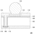
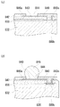
図1は、本実施の形態に係る半導体装置を模式的に示した断面図である。図1の上方向は半導体基板の裏面方向であり、図1の下方向は半導体基板の素子形成面方向である。 FIG. 1 is a cross-sectional view schematically showing a semiconductor device according to the present embodiment. The upper direction in FIG. 1 is the back surface direction of the semiconductor substrate, and the lower direction in FIG. 1 is the element formation surface direction of the semiconductor substrate.
本実施形態に係る半導体装置100は、シリコン基板などの半導体基板102の表面側にSiO2膜などの絶縁膜104を備える。半導体基板102の膜厚は通常10μm以上100μm以下程度である。なお、この膜厚のシリコン基板は、通常の膜厚の半導体基板の裏面を研磨することにより得ることもできる。絶縁膜104中には、アルミニウムパッドやアルミニウム配線などからなる電極106が設けられている。
The
半導体基板102には、半導体基板102の表面側と裏面側とに開口部を有する貫通孔が設けられている。この貫通孔内部および半導体基板102の裏面には、SiO2膜などからなる絶縁膜108が設けられている。絶縁膜108の裏面の一部には、アクリル系樹脂112のパッドが設けられている。
The
絶縁膜108の裏面、アクリル系樹脂112の裏面および貫通孔中の絶縁膜108の内面には、例えばアルミニウム配線または銅配線などからなる再配線110が形成されている。
A rewiring 110 made of, for example, aluminum wiring or copper wiring is formed on the back surface of the insulating
上記貫通孔中心部、アクリル系樹脂112の裏面および絶縁膜108の裏面には、ラミネートタイプフォトソルダーレジスト膜114が設けられている。ラミネートタイプフォトソルダーレジスト膜114の一部に、アクリル系樹脂112上の再配線110に達する開口部が設けられており、この開口部内部に半田ボール116が形成されている。
A laminate type photo solder resist
絶縁膜108および再配線110は貫通孔を貫通して、半導体基板102の表面側に一部が存在しており、その部分は電極106と接している。電極106と半導体基板102との残りの間隙にはSiO2膜などからなる絶縁膜118が存在している。
The insulating
このように、本実施形態の半導体装置100は、半導体基板102の素子形成面に設けられた半田ボール116と、裏面に設けられた電極106とを接続するため、半導体装置100の3次元実装が容易になり、半導体装置のさらなる高集積化を実現できる。
As described above, since the
本実施形態では、フォトソルダーレジスト膜は、ネガ型であってもポジ型であってもよい。もっとも、カルド型ポリマーがカルボン酸基とアクリレート基とを同一分子鎖内に有する場合には、一般にはネガ型のフォトソルダーレジスト膜として用いられる。ここで、ネガ型のフォトソルダーレジスト膜とは、具体的には、感光した部分だけを構造変化させ、溶媒に溶けなくする感光性樹脂を使った絶縁用被膜を意味する。一般には、ハンダ付けの際に用いられるため、耐熱性や高弾性などの優れた耐久性が求められる。本実施形態では、このような特性を満たすために、後述する特定のポリマーを含有するネガ型のフォトソルダーレジスト膜を用いている。 In the present embodiment, the photo solder resist film may be a negative type or a positive type. However, when the cardo type polymer has a carboxylic acid group and an acrylate group in the same molecular chain, it is generally used as a negative type photo solder resist film. Here, the negative-type photo solder resist film specifically means an insulating film using a photosensitive resin that changes the structure of only the exposed portion and does not dissolve in the solvent. Generally, since it is used for soldering, excellent durability such as heat resistance and high elasticity is required. In this embodiment, in order to satisfy such characteristics, a negative type photo solder resist film containing a specific polymer described later is used.
なお、ラミネートタイプフォトソルダーレジスト膜とは、通常の液状の原液を塗布してなるフォトソルダーレジスト膜とは異なり、薄膜状のフォトソルダーレジスト膜を接着してなるラミネートタイプのフォトソルダーレジスト膜である。この際、フォトソルダーレジスト膜はある程度軟化した状態で適当な温度、圧力条件下で半導体基板などに接着される。 The laminate type photo solder resist film is a laminate type photo solder resist film formed by bonding a thin photo solder resist film, unlike a photo solder resist film formed by applying a normal liquid stock solution. . At this time, the photo solder resist film is bonded to a semiconductor substrate or the like under appropriate temperature and pressure conditions in a state of being softened to some extent.
また、ラミネートタイプフォトソルダーレジスト膜114の接着前の材料フィルムの膜厚は、特に限定するものではないが、例えば25μm以上とすることができ、特に好ましくは35μm以上である。また、材料フィルムを接着して得られるラミネートタイプフォトソルダーレジスト膜114の膜厚は、例えば20μm以上とすることができ、特に好ましくは30μm以上である。材料フィルムまたはラミネートタイプフォトソルダーレジスト膜114の膜厚がこれらの範囲であれば、絶縁性および機械的強度が向上する。
Moreover, the film thickness of the material film before adhesion of the laminate type photo solder resist
また、ラミネートタイプフォトソルダーレジスト膜114の接着前の材料フィルムの膜厚は、例えば100μm以下とすることができ、特に好ましくは50μm以下である。また、材料フィルムを接着して得られるラミネートタイプフォトソルダーレジスト膜114の膜厚は、例えば90μm以下とすることができ、特に好ましくは45μm以下である。材料フィルムまたはラミネートタイプフォトソルダーレジスト膜114の膜厚がこれらの範囲であれば、ラミネートタイプフォトソルダーレジスト膜114の接着の際の圧力も小さくてすみ、半導体装置100にかかるストレスも抑制できる。また、ラミネートタイプフォトソルダーレジスト膜114の膜厚が薄いため、UV照射による光硬化処理などの際の加工性が良好となる。
Moreover, the film thickness of the material film before adhesion of the laminate type photo solder resist
なお、このような通常のラミネートタイプフォトソルダーレジスト膜よりも薄いラミネートタイプフォトソルダーレジスト膜114を実現するためには、後述する特定の構造を有するカルド型ポリマーを用いることが有効である。後述するカルド型ポリマーは加工性が良好であるため、優れた絶縁性を有する薄膜を形成可能だからである。
In order to realize such a laminate type photo solder resist
そして、上記ラミネートタイプフォトソルダーレジスト膜114は、カルド型ポリマーを含有してもよい。カルド型ポリマーとは、式(I)に示すように、環状の基がポリマー主鎖に直接結合した構造を有するポリマーの総称である。
The laminate type photo solder resist
なお、式(I)において、R1、R2はアルキル基、ベンジル基などの二価の基を表す。 In formula (I), R 1 and R 2 represent a divalent group such as an alkyl group or a benzyl group.
すなわち、このカルド型ポリマーとは、四級炭素を有する嵩高い置換基が、主鎖に対して、ほぼ直角に存在する構造を有しているポリマーのことである。 That is, the cardo type polymer is a polymer having a structure in which a bulky substituent having a quaternary carbon is present substantially perpendicular to the main chain.
ここで、環状部は、飽和結合でも不飽和結合を含んでいてもよく、炭素の他、窒素原子、酸素原子、硫黄原子、リン原子等の原子を含んでいてもよい。また、環状部は多環であってもよく、縮合環であってもよい。また、環状部は、他の炭素鎖と結合していても、更には、架橋していてもよい。 Here, the cyclic portion may include a saturated bond or an unsaturated bond, and may include atoms such as a nitrogen atom, an oxygen atom, a sulfur atom, and a phosphorus atom in addition to carbon. The cyclic part may be a polycycle or a condensed ring. Moreover, even if the cyclic part is couple | bonded with the other carbon chain, it may be bridge | crosslinked further.
なお、嵩高い置換基としては、たとえば、式(II)に示すように、五員環の両側に六員環が結合し、五員環の残り一つの炭素原子が主鎖と結合した構造を有する縮合環を有するフルオレニル基などの環状の基が挙げられる。 As the bulky substituent, for example, as shown in the formula (II), a structure in which a six-membered ring is bonded to both sides of the five-membered ring and the remaining one carbon atom of the five-membered ring is bonded to the main chain. And cyclic groups such as a fluorenyl group having a condensed ring.
フルオレニル基とは、フルオレンの9位の炭素原子が脱水素化された基であり、カルド型ポリマーにおいては、式(I)に示すように、脱水素化された炭素原子の位置で、主鎖であるアルキル基の炭素原子と結合している。 The fluorenyl group is a group in which the 9th carbon atom of fluorene is dehydrogenated. In the cardo type polymer, as shown in the formula (I), the main chain is located at the position of the dehydrogenated carbon atom. It is bonded to the carbon atom of the alkyl group.
カルド型ポリマーは、上記構造を有するポリマーであるため、
(1)ポリマー主鎖の回転拘束
(2)主鎖及び側鎖のコンフォメーション規制
(3)分子間パッキングの阻害
(4)側鎖の芳香族置換基導入等による芳香族性の増加
といった効果を奏する。
Since the cardo type polymer is a polymer having the above structure,
(1) Rotation constraint of polymer main chain (2) Conformation regulation of main chain and side chain (3) Inhibition of intermolecular packing (4) Effect of increasing aromaticity by introduction of aromatic substituent on side chain Play.
したがって、カルド型ポリマーは、高耐熱性、溶剤溶解性、高透明性、高屈折率、低複屈折率、更には、より高い気体透過性といった特徴を有する。 Therefore, the cardo type polymer has characteristics such as high heat resistance, solvent solubility, high transparency, high refractive index, low birefringence, and higher gas permeability.
また、上記カルド型ポリマーに、所定の改質剤を導入することによって、ボイドの発生を抑制した状態で薄膜化した材料フィルムを得ることができる。そして、このようにボイドの発生を抑制した状態で薄膜化した材料フィルムを接着することにより、ボイドの少ないラミネートタイプフォトソルダーレジスト膜114が得られる。そのため、半導体装置100の信頼性および製造安定性が向上する。
In addition, by introducing a predetermined modifier into the cardo polymer, a material film that has been thinned in a state in which generation of voids is suppressed can be obtained. Then, the laminated type photo solder resist
また、カルド型ポリマーは、機械的強度および耐熱性に優れる。そして、カルド型ポリマーを含有するラミネートタイプフォトソルダーレジスト膜114は、機械的強度および耐熱性に優れる。よって、半導体装置100の信頼性および製造安定性が向上する。
The cardo type polymer is excellent in mechanical strength and heat resistance. The laminate type photo solder resist
なお、上記カルド型ポリマーは、カルボン酸基とアクリレート基とを同一分子鎖内に有するポリマーが架橋してなるポリマーであってもよい。従来の一般的な感光性ワニスとしては、現像性を持つカルボン酸基オリゴマーと多官能アクリルとのブレンドが用いられているが、解像度の面でさらなる改善の余地があった。一般的な感光ワニスの代わりに、カルボン酸基とアクリレート基とを同一分子鎖内に有するポリマーが架橋してなるカルド型ポリマーを用いると、現像性を持つカルボン酸と架橋基であるアクリレート基とを同一分子鎖中に有し、主鎖に嵩高い置換基を持ちラジカル拡散し難いため、カルド型ポリマーを含有するフォトソルダーレジスト膜328の解像度が向上する利点がある。 The cardo type polymer may be a polymer obtained by crosslinking a polymer having a carboxylic acid group and an acrylate group in the same molecular chain. As a conventional general photosensitive varnish, a blend of a carboxylic acid group oligomer having developability and a polyfunctional acrylic is used, but there is room for further improvement in terms of resolution. In place of a general photosensitive varnish, if a cardo type polymer obtained by crosslinking a polymer having a carboxylic acid group and an acrylate group in the same molecular chain is used, a developable carboxylic acid and an acrylate group which is a crosslinking group In the same molecular chain and has a bulky substituent in the main chain and is difficult to radically diffuse. Therefore, there is an advantage that the resolution of the photo solder resist film 328 containing a cardo type polymer is improved.
また、上記カルド型ポリマーを含むフォトソルダーレジスト膜114は、以下に示す諸物性値を満たすことが望ましい。なお、以下の物性値はフィラーなどを含まない樹脂部分についての値であり、フィラーなどを添加することにより、適宜調整可能である。
Further, it is desirable that the photo solder resist
ここで、上記カルド型ポリマーを含むフォトソルダーレジスト膜114のガラス転移温度(Tg)は、例えば180℃以上とすることができ、特に好ましくは190℃以上である。ガラス転移温度がこの範囲にあると、カルド型ポリマーを含むラミネートタイプフォトソルダーレジスト膜114の耐熱性が向上する。
Here, the glass transition temperature (Tg) of the photo solder resist
また、上記カルド型ポリマーを含むフォトソルダーレジスト膜114のガラス転移温度(Tg)は、例えば220℃以下とすることができ、特に好ましくは210℃以下である。ガラス転移温度がこの範囲であれば、通常の製法により安定的に製造可能である。ガラス転移温度は、例えばバルク試料の動的粘弾性測定(DMA)により測定可能である。
In addition, the glass transition temperature (Tg) of the photo solder resist
また、上記カルド型ポリマーを含むフォトソルダーレジスト膜114のTg以下の領域における線膨張係数(CTE)は、例えば80ppm/℃以下とすることができ、特に好ましくは75ppm/℃以下である。また、上記ポリマーにフィラーを配合し、熱膨張係数を20ppm/℃以下の樹脂組成物を得ることもできる。線膨張係数がこの範囲にあると、カルド型ポリマーを含むラミネートタイプフォトソルダーレジスト膜114と、再配線110などとの密着性が向上する。
Moreover, the linear expansion coefficient (CTE) in the area | region below Tg of the photo solder resist
また、上記カルド型ポリマーを含むフォトソルダーレジスト膜114のTg以下の領域における線膨張係数(CTE)は、例えば50ppm/℃以上とすることができ、特に好ましくは55ppm/℃以上である。線膨張係数がこの範囲であれば、通常の製法により安定的に製造可能である。線膨張係数は、例えば熱機械分析装置(TMA)による熱膨張測定により測定可能である。
Moreover, the linear expansion coefficient (CTE) in the area | region below Tg of the photo solder resist
また、上記カルド型ポリマーを含むフォトソルダーレジスト膜114の熱伝導率は、例えば0.50W/cm2・sec以下とすることができ、特に好ましくは0.35W/cm2・sec以下である。熱伝導率がこの範囲にあると、カルド型ポリマーを含むラミネートタイプフォトソルダーレジスト膜114の耐熱性が向上する。
Further, the thermal conductivity of the photo solder resist
また、上記カルド型ポリマーを含むフォトソルダーレジスト膜114の熱伝導率は、例えば0.10W/cm2・sec以上とすることができ、特に好ましくは0.25W/cm2・sec以上である。熱伝導率がこの範囲であれば、通常の製法により安定的に製造可能である。熱伝導率は、例えば円板熱流計法(ASTM E1530)により測定可能である。
The thermal conductivity of the photo solder resist
また、上記カルド型ポリマーを含むフォトソルダーレジスト膜114の10〜100μm直径のビアにおけるビアアスペクト比は、例えば0.5以上とすることができ、特に好ましくは1以上である。ビアアスペクト比がこの範囲にあると、カルド型ポリマーを含むラミネートタイプフォトソルダーレジスト膜114の解像度が向上する。
In addition, the via aspect ratio of the 10 to 100 μm diameter via of the photo solder resist
また、上記カルド型ポリマーを含むフォトソルダーレジスト膜114の10〜100μm直径のビアにおけるビアアスペクト比は、例えば5以下とすることができ、特に好ましくは2以下である。ビアアスペクト比がこの範囲であれば、通常の製法により安定的に製造可能である。
Further, the via aspect ratio of the photo solder resist
また、上記カルド型ポリマーを含むフォトソルダーレジスト膜114において、周波数1MHzの交流電界を印加した場合の誘電率は、例えば4以下とすることができ、特に好ましくは3以下である。誘電率がこの範囲にあると、カルド型ポリマーを含むラミネートタイプフォトソルダーレジスト膜114の高周波特性をはじめとする誘電特性が向上する。
In the photo solder resist
また、上記カルド型ポリマーを含むフォトソルダーレジスト膜114において、周波数1MHzの交流電界を印加した場合の誘電率は、例えば0.1以上とすることができ、特に好ましくは2.7以上である。誘電率がこの範囲であれば、通常の製法により安定的に製造可能である。
In the photo solder resist
また、上記カルド型ポリマーを含むフォトソルダーレジスト膜114において、周波数1MHzの交流電界を印加した場合の誘電正接は、例えば0.04以下とすることができ、特に好ましくは0.029以下である。誘電正接がこの範囲にあると、カルド型ポリマーを含むラミネートタイプフォトソルダーレジスト膜114の高周波特性をはじめとする誘電特性が向上する。
Further, in the photo solder resist
また、上記カルド型ポリマーを含むフォトソルダーレジスト膜114において、周波数1MHzの交流電界を印加した場合の誘電正接は、例えば0.001以上とすることができ、特に好ましくは0.027以上である。誘電正接がこの範囲であれば、通常の製法により安定的に製造可能である。
Further, in the photo solder resist
また、上記カルド型ポリマーを含むフォトソルダーレジスト膜114において、24時間吸水率(wt%)は、例えば3wt%以下とすることができ、特に好ましくは1.5wt%以下である。24時間吸水率(wt%)がこの範囲にあると、カルド型ポリマーを含むフォトソルダーレジスト膜328の耐湿性を向上することができる。
Further, in the photo solder resist
また、上記カルド型ポリマーを含むフォトソルダーレジスト膜114において、24時間吸水率(wt%)は、例えば0.5wt%以上とすることができ、特に好ましくは1.3wt%以上である。24時間吸水率(wt%)がこの範囲であれば、通常の製法により安定的に製造可能である。
Further, in the photo solder resist
これら上記の複数の特性を上記カルド型ポリマーを含むフォトソルダーレジスト膜114が満たす場合には、機械的強度、耐熱性、他の部材との密着性、解像度、誘電特性、耐湿性などの諸特性がバランス良く実現される。そのため、信頼性および耐熱性に優れ、半導体素子を搭載する際の位置精度に優れる半導体装置が安定的に提供される。
When the above-mentioned plurality of characteristics are satisfied by the photo solder resist
<実施形態2> <Embodiment 2>
図2〜図6は、本実施の形態に係る半導体装置の製造方法を示した工程断面図である。図2〜図6の上方向は半導体基板の裏面方向であり、図2〜図6の下方向は半導体基板の素子形成面方向である。 2 to 6 are process cross-sectional views illustrating a method for manufacturing a semiconductor device according to the present embodiment. 2 to 6 is the rear surface direction of the semiconductor substrate, and the lower direction of FIGS. 2 to 6 is the element formation surface direction of the semiconductor substrate.
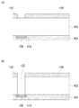
上述の実施形態1に示したような半導体装置を得るためには、まず、図2(a)に示すように、シリコン基板などからなる半導体基板102の表面にSiO2膜などからなる絶縁膜118とアルミニウムパッドなどからなる電極106とをこの順に積層し、所定の形状となるようにパターニングする。そして、この絶縁膜118と電極106との積層膜および半導体基板102の表面などを覆うSiO2などからなる絶縁膜104を形成する。さらに、半導体基板102の裏面側にはレジスト膜120を形成する。レジスト膜120には所定の開口部を設けておく。
In order to obtain the semiconductor device as shown in the first embodiment, first, as shown in FIG. 2A, an insulating
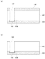
次いで、図2(b)に示すように、レジスト膜120をマスクとして半導体基板102のドライエッチングを行い、絶縁膜118の裏面に達する貫通孔122を形成する。さらに、図3(c)に示すように、エッチングガスを変えてさらに絶縁膜118をドライエッチングして、貫通孔122を電極106の裏面に到達させる。そして、図3(d)に示すように、レジスト膜120を除去する。
Next, as shown in FIG. 2B, the
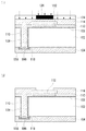
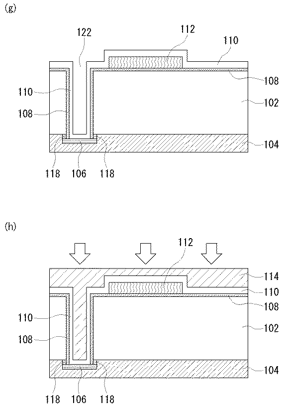
続いて、図4(e)に示すように、貫通孔122内に設けられた絶縁膜108の内面および半導体基板102の裏面などを覆うSiO2膜などからなる絶縁膜108を形成する。さらに、図4(f)に示すように、貫通孔122の底面の絶縁膜108を指向性スパッタリングなどの手法により除去する。
Subsequently, as shown in FIG. 4E, an insulating
そして、図5(g)に示すように、絶縁膜108の所定の位置にアクリル系樹脂112のパッドを形成する。さらに、貫通孔122の内面、貫通孔122の裏面および絶縁膜108の裏面を覆うアルミニウム配線または銅配線などからなる再配線110を形成する。
Then, as shown in FIG. 5G, a pad of
次いで、図5(h)に示すように、貫通孔122内に設けられた再配線110の内面および半導体基板102の裏面の再配線110の裏面などを覆う、カルド型ポリマーを含有しているラミネートタイプフォトソルダーレジスト膜114を接着する。接着の際にかかる圧力の方向を矢印で図示する。
Next, as shown in FIG. 5 (h), a laminate containing a cardo type polymer covering the inner surface of the
続いて、図6(i)に示すように、ラミネートタイプフォトソルダーレジスト膜114の裏面に遮光領域126を有するフォトマスク124を形成する。そして、UV光などをフォトマスク124を通してラミネートタイプフォトソルダーレジスト膜114に照射することにより、ラミネートタイプフォトソルダーレジスト膜114の照射領域において上述のカルド型ポリマーのアクリレート基を架橋させてアクリル基を形成する。
Subsequently, as shown in FIG. 6I, a
なお、カルド型ポリマーを含有するラミネートタイプフォトソルダーレジスト膜114は、一般的に、上記露光・現像工程とは別に、適当な条件によるアフターベーク工程により硬化させることにより、上記の望ましい諸特性を備えるようになる。
In addition, the laminate type photo solder resist
その後、図6(j)に示すように、フォトマスク124を除去後、ラミネートタイプフォトソルダーレジスト膜114をエッチングして、ラミネートタイプフォトソルダーレジスト膜114の露光・現像していない領域を除去する。
Thereafter, as shown in FIG. 6 (j), after removing the
そして、得られたラミネートタイプフォトソルダーレジスト膜114の開口部に半田ボール116を形成して再配線110と接続させることにより、図1に示した構成からなる実施形態1に係る半導体装置100を得る。
Then, the
本実施形態に係る半導体装置100の製造方法では、接着により貫通孔122内に設けられた再配線110の内面、および半導体基板102の裏面の再配線110の裏面などにラミネートタイプフォトソルダーレジスト膜114を密着させる。
In the manufacturing method of the
ここで、ラミネートタイプフォトソルダーレジスト膜114の接着前の材料フィルムは、カルド型ポリマーと所定の添加剤とを用いて、ボイドや凹凸などの発生が抑制された状態で薄膜に成形可能である。また、カルド型ポリマーを含む材料フィルムは、加熱することにより材料を軟化することが容易なため、埋め込み性が良く、接着された半導体装置100のラミネートタイプフォトソルダーレジスト膜114にもボイドや凹凸は少ない。そして、ボイドが少ないラミネートタイプフォトソルダーレジスト膜114によれば、膜厚が保障できる。
Here, the material film before adhesion of the laminate type photo solder resist
一方、上記の特許文献1に示した、スピンコート法により形成されたフォトソルダーレジスト膜を用いた半導体装置は、半田ボールを配置するピッチの微細化が進むとともに、フォトソルダーレジスト膜の埋め込み特性が充分ではなくなる場合があった。そのため、再配線パターンの側壁またはビア底でボイド(空洞)が発生する場合があった。半導体装置の絶縁保障などの信頼性の点でさらなる改善の余地があった。 On the other hand, the semiconductor device using the photo solder resist film formed by the spin coat method shown in the above-mentioned Patent Document 1 has a finer pitch for arranging the solder balls, and has an embedding characteristic of the photo solder resist film. Sometimes it was not enough. For this reason, a void (cavity) may occur on the side wall or via bottom of the rewiring pattern. There was room for further improvement in terms of reliability, such as ensuring insulation of semiconductor devices.
なお、本発明者らは、3次元実装を実現するために、シリコン基板に貫通電極を形成して端子電極を基板裏面側に取り出すような構造のWL−CSPも発明している。このようなシリコン貫通電極を備えたWL−CSPの場合には、上述のように、貫通電極部分に大きなボイドが形成される場合がある。 In order to realize three-dimensional mounting, the inventors have also invented a WL-CSP having a structure in which a through electrode is formed on a silicon substrate and a terminal electrode is taken out to the back side of the substrate. In the case of a WL-CSP provided with such a silicon through electrode, a large void may be formed in the through electrode portion as described above.
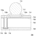
図7は、液状のフォトソルダーレジスト膜を塗布してなる半導体装置を模式的に示した断面図である。 FIG. 7 is a cross-sectional view schematically showing a semiconductor device formed by applying a liquid photo solder resist film.
この場合には、塗布フォトソルダーレジスト膜714を形成するために、液状のフォトソルダーレジスト膜原液をスピンコート法などにより半導体基板702の裏面に設けられた再配線710の裏面などに塗布するが、貫通孔内に設けられた再配線710の内面の空間にはフォトソルダーレジスト膜を充填することが困難である。また、再配線710が曲折している箇所には、液状のフォトソルダーレジスト膜原液が塗布されない領域が生じる場合がある。このため、ボイド730a、730b、730cまたは凹凸などが生じる場合がある。このようなボイド730a、730b、730cまたは凹凸が発生すると、半導体装置700の信頼性または製造安定性が低下する場合がある。
In this case, in order to form the coated photo solder resist
また、上記の特許文献2に記載した、ドライフィルム型の感光性フォトソルダーレジスト膜をラミネートしてコーティングした場合には、フォトソルダーレジスト膜の膜厚が50μm程度と厚くなってしまうため、フォトソルダーレジスト膜の接着時に半導体装置にかかるストレスやフォトソルダーレジスト膜の加工性などの製造安定性の点で改善の余地があった。 In addition, when the dry film type photosensitive photo solder resist film described in Patent Document 2 is laminated and coated, the thickness of the photo solder resist film becomes as thick as about 50 μm. There was room for improvement in terms of manufacturing stability such as stress applied to the semiconductor device during adhesion of the resist film and processability of the photo solder resist film.
これに対して、本実施形態の半導体装置100の製造方法においては、液状のフォトソルダーレジスト膜原液を塗布してフォトソルダーレジスト膜を形成する代わりに、ラミネートタイプフォトソルダーレジスト膜114を接着する。
On the other hand, in the manufacturing method of the
ここで、ラミネートタイプフォトソルダーレジスト膜114の材料フィルムは、カルド型ポリマーおよび所定の添加剤を用いて成形されるので、ボイドや凹凸などの発生を抑制した状態で薄膜成形できる。そして、カルド型ポリマーを含む材料フィルムは、加熱により材料を軟化することが容易なため、埋め込み性がよい。そのため、液状のフォトソルダーレジスト膜原液をスピンコート法などにより塗布する場合に比べて、信頼性に優れる半導体装置100を安定的に製造可能である。
Here, since the material film of the laminate type photo solder resist
また、上述のカルド型ポリマーを含有するラミネートタイプフォトソルダーレジスト膜114を用いる場合には、ラミネートタイプフォトソルダーレジスト膜114の耐熱性および加工性はさらに良好となる。さらに、上述のカルド型ポリマーを含有するラミネートタイプフォトソルダーレジスト膜114は、薄くても解像度が優れているため、フォトソルダーレジスト膜の接着時に半導体装置にかかるストレスを抑制できる。また、上述のカルド型ポリマーを含有するラミネートタイプフォトソルダーレジスト膜114の材料フィルムは、薄くても機械的強度に優れるため、加工性の面でも優れている。
Further, when the laminate type photo solder resist
また、このようにラミネートタイプフォトソルダーレジスト膜114の材料フィルムは、薄くても機械的強度に優れ、加工性に優れるため、材料フィルムの膜厚を薄くすることができる。さらに、一定温度に加熱することにより材料フィルムを容易に軟化することができるため、貫通孔内に設けられた再配線710の内面の空間にはフォトソルダーレジスト膜114の材料フィルムを容易に埋め込むことができる。
Moreover, since the material film of the laminate type photo solder resist
一方、液状の原料液を用いてスピンコート法によりソルダーレジスト膜を形成する場合には、ソルダーレジスト膜の外周部などにボイドが生じやすく、半田ボール間の絶縁保障に難点がある場合もある。これに対して、フィルムタイプのソルダーレジスト膜の材料フィルムを用いれば、接着前にボイドの有無の検査が可能となる。このため、フィルムタイプのソルダーレジスト膜の材料フィルムを接着すれば、半田ボール間の絶縁保障が良好となり、信頼性に優れる半導体装置が得られる。 On the other hand, when a solder resist film is formed by a spin coating method using a liquid raw material liquid, voids are likely to occur in the outer periphery of the solder resist film, and there may be a difficulty in ensuring insulation between solder balls. On the other hand, if a material film of a film type solder resist film is used, the presence or absence of voids can be inspected before bonding. For this reason, if a material film of a film type solder resist film is adhered, insulation between the solder balls is improved and a semiconductor device having excellent reliability can be obtained.
以上、本発明の構成について説明したが、これらの構成を任意に組み合わせたものも本発明の態様として有効である。また、本発明の表現を他のカテゴリーに変換したものもまた本発明の態様として有効である。 As mentioned above, although the structure of this invention was demonstrated, what combined these structures arbitrarily is effective as an aspect of this invention. Moreover, what converted the expression of this invention into the other category is also effective as an aspect of this invention.
例えば、上記の実施形態では、外部接続端子として半田ボール116を用いたが、特に限定する趣旨ではない。例えば、外部接続端子は、電極パッドであってもよく、別のアルミニウム配線または銅配線などであってもよい。
For example, in the above-described embodiment, the
また、上記の実施形態では、半田ボール116を形成するときの外力を緩和し、半田ボール116と再配線110とのコンタクト性を向上させるために、アクリル系樹脂112のパッドを設けたが、特にアクリル系樹脂112を設ける必要はない。例えば、全くパッドを設けなくてもよいし、アクリル系樹脂以外の樹脂からなるパッドを設けてもよい。
In the above embodiment, the pad of the
100 半導体装置
102 半導体基板
106 電極
108 絶縁膜
110 再配線
112 アクリル系樹脂
114 ラミネートタイプフォトソルダーレジスト膜
116 半田ボール
120 レジスト膜
122 貫通孔
124 フォトマスク
126 遮光領域
124 フォトマスク
126 遮光領域
700 半導体装置
702 半導体基板
706 電極
708 絶縁膜
710 再配線
712 アクリル系樹脂
714 塗布フォトソルダーレジスト膜
716 半田ボール
730 ボイド
832 半導体チップ
834 パッシベーション膜
836 電極
838 絶縁シート
840 金属層
842 絶縁皮膜
843 外部端子接合部
844 透孔
846 外部接続端子
850 紫外線遮蔽層
880 ボイド発生部位
1001 表面実装部品パッド
1002 CSPパッド
1003 ランド
1004 ソルダーレジスト
1005 フォトマスク
1006 紫外線
1007 ソルダーレジスト開口部
1008 炭酸ガスレーザ
1009 ソルダーレジスト開口部
1010 半田ペースト
DESCRIPTION OF
Claims (6)
前記基板の一方の面に設けられている第一の導電部材と、
少なくとも一部が前記基板の接続孔内の一部に設けられており、前記第一の導電部材と接続する第二の導電部材と、
少なくとも一部が前記基板の接続孔内の一部および前記基板の他方の面に設けられている絶縁膜と、
を備え、
前記絶縁膜は、カルド型ポリマーを含有することを特徴とする半導体装置。 A substrate having a connection hole opening in one surface and the other surface;
A first conductive member provided on one surface of the substrate;
A second conductive member connected to the first conductive member, at least part of which is provided in a part of the connection hole of the substrate;
An insulating film provided at least in part on a part of the connection hole of the substrate and the other surface of the substrate;
With
The semiconductor device, wherein the insulating film contains a cardo type polymer.
前記カルド型ポリマーは、カルボン酸基とアクリレート基とを同一分子鎖内に有するポリマーが架橋してなることを特徴とする半導体装置。 The semiconductor device according to claim 1,
The cardo type polymer is formed by crosslinking a polymer having a carboxylic acid group and an acrylate group in the same molecular chain.
前記絶縁膜は、ドライフィルム型のフォトソルダーレジスト膜の材料フィルムを接着してなることを特徴とする半導体装置。 The semiconductor device according to claim 1 or 2,
The insulating film is formed by adhering a material film of a dry film type photo solder resist film.
前記絶縁膜のガラス転移温度が180℃以上220℃以下であり、
前記絶縁膜の周波数1MHzの交流電界を印加した場合の誘電正接が0.001以上0.04以下であることを特徴とする半導体装置。 The semiconductor device according to claim 1,
The glass transition temperature of the insulating film is 180 ° C. or higher and 220 ° C. or lower,
2. A semiconductor device, wherein a dielectric loss tangent is 0.001 or more and 0.04 or less when an AC electric field having a frequency of 1 MHz is applied to the insulating film.
前記絶縁膜のガラス転移温度以下の領域における線膨張係数が50ppm/℃以上80ppm/℃以下であることを特徴とする半導体装置。 The semiconductor device according to claim 4,
A linear expansion coefficient of the insulating film in a region below the glass transition temperature is from 50 ppm / ° C. to 80 ppm / ° C.
基板の一方の面と他方の面とに開口する接続孔を形成する工程と、
少なくとも一部が前記基板の接続孔内の一部に存在するように、前記第一の導電部材と接続する第二の導電部材を形成する工程と、
少なくとも一部が前記基板の接続孔内の一部および前記基板の他方の面に存在するように、カルド型ポリマーを含有する絶縁フィルムを接着して絶縁膜を形成する工程と、
を含むことを特徴とする半導体装置の製造方法。 Forming a first conductive member on one side of the substrate;
Forming a connection hole opening in one surface and the other surface of the substrate;
Forming a second conductive member to be connected to the first conductive member so that at least a part thereof exists in a part of the connection hole of the substrate;
Bonding an insulating film containing a cardo-type polymer to form an insulating film so that at least a part is present in a part of the connection hole of the substrate and the other surface of the substrate;
A method for manufacturing a semiconductor device, comprising:
Priority Applications (1)
| Application Number | Priority Date | Filing Date | Title |
|---|---|---|---|
| JP2004103218A JP2005294320A (en) | 2004-03-31 | 2004-03-31 | Semiconductor device and manufacturing method thereof |
Applications Claiming Priority (1)
| Application Number | Priority Date | Filing Date | Title |
|---|---|---|---|
| JP2004103218A JP2005294320A (en) | 2004-03-31 | 2004-03-31 | Semiconductor device and manufacturing method thereof |
Publications (1)
| Publication Number | Publication Date |
|---|---|
| JP2005294320A true JP2005294320A (en) | 2005-10-20 |
Family
ID=35326958
Family Applications (1)
| Application Number | Title | Priority Date | Filing Date |
|---|---|---|---|
| JP2004103218A Pending JP2005294320A (en) | 2004-03-31 | 2004-03-31 | Semiconductor device and manufacturing method thereof |
Country Status (1)
| Country | Link |
|---|---|
| JP (1) | JP2005294320A (en) |
Cited By (7)
| Publication number | Priority date | Publication date | Assignee | Title |
|---|---|---|---|---|
| JP2009182208A (en) * | 2008-01-31 | 2009-08-13 | Kyushu Institute Of Technology | Semiconductor chip package and manufacturing method thereof |
| JP2010045162A (en) * | 2008-08-12 | 2010-02-25 | Toshiba Corp | Semiconductor device, method of manufacturing semiconductor device, and camera module |
| WO2011086612A1 (en) * | 2010-01-15 | 2011-07-21 | パナソニック株式会社 | Semiconductor device |
| CN102376629A (en) * | 2010-08-17 | 2012-03-14 | 中国科学院上海微系统与信息技术研究所 | A Method for Realizing Through-Silicon Via Interconnection Using Suspension Photoresist |
| JP2012160761A (en) * | 2012-05-16 | 2012-08-23 | Fujikura Ltd | Semiconductor device |
| EP2584598A1 (en) * | 2011-10-20 | 2013-04-24 | austriamicrosystems AG | Method of producing a semiconductor device comprising a through-substrate via and a capping layer and corresponding semiconductor device |
| US9099536B2 (en) | 2012-05-25 | 2015-08-04 | Lapis Semiconductor Co., Ltd. | Semiconductor device and method of producing semiconductor device |
-
2004
- 2004-03-31 JP JP2004103218A patent/JP2005294320A/en active Pending
Cited By (12)
| Publication number | Priority date | Publication date | Assignee | Title |
|---|---|---|---|---|
| JP2009182208A (en) * | 2008-01-31 | 2009-08-13 | Kyushu Institute Of Technology | Semiconductor chip package and manufacturing method thereof |
| JP2010045162A (en) * | 2008-08-12 | 2010-02-25 | Toshiba Corp | Semiconductor device, method of manufacturing semiconductor device, and camera module |
| US8426977B2 (en) | 2008-08-12 | 2013-04-23 | Kabushiki Kaisha Toshiba | Semiconductor apparatus, manufacturing method of semiconductor apparatus, and camera module |
| WO2011086612A1 (en) * | 2010-01-15 | 2011-07-21 | パナソニック株式会社 | Semiconductor device |
| US8450836B2 (en) | 2010-01-15 | 2013-05-28 | Panasonic Corporation | Semiconductor device |
| CN102376629A (en) * | 2010-08-17 | 2012-03-14 | 中国科学院上海微系统与信息技术研究所 | A Method for Realizing Through-Silicon Via Interconnection Using Suspension Photoresist |
| EP2584598A1 (en) * | 2011-10-20 | 2013-04-24 | austriamicrosystems AG | Method of producing a semiconductor device comprising a through-substrate via and a capping layer and corresponding semiconductor device |
| JP2012160761A (en) * | 2012-05-16 | 2012-08-23 | Fujikura Ltd | Semiconductor device |
| US9099536B2 (en) | 2012-05-25 | 2015-08-04 | Lapis Semiconductor Co., Ltd. | Semiconductor device and method of producing semiconductor device |
| US9892995B2 (en) | 2012-05-25 | 2018-02-13 | Lapis Semiconductor Co., Ltd. | Semiconductor device |
| US10153228B2 (en) | 2012-05-25 | 2018-12-11 | Lapis Semiconductor Co., Ltd. | Semiconductor device |
| US10580721B2 (en) | 2012-05-25 | 2020-03-03 | Lapis Semiconductor Co., Ltd. | Semiconductor device |
Similar Documents
| Publication | Publication Date | Title |
|---|---|---|
| JP5158212B2 (en) | Positive photosensitive resin composition, method for producing resist pattern, semiconductor device and electronic device | |
| TWI330392B (en) | Semiconductor device, manufacturing method of the semiconductor device, and mounting method of the semiconductor device | |
| TWI224487B (en) | Interposer for chip size package and method for manufacturing the same | |
| TW201131668A (en) | Method for manufacturing electronic device, electronic device, method for manufacturing electronic device package and electronic device package | |
| CN1341279A (en) | Semiconductor device | |
| JP4736863B2 (en) | Positive photosensitive polyamideimide resin composition, pattern manufacturing method, and electronic component | |
| TW201335703A (en) | Photosensitive resin composition, manufacturing method of cured film pattern and electronic component | |
| KR100833706B1 (en) | Photosensitive polyimide composition, polyimide film and semiconductor device using the same | |
| JP2005294320A (en) | Semiconductor device and manufacturing method thereof | |
| TWI255491B (en) | Substrate for mounting elements, manufacturing method therefor and semiconductor device using the same | |
| TWI872143B (en) | Photosensitive resin composition, method for selecting photosensitive resin composition, method for producing patterned cured film, and method for producing semiconductor device | |
| JP4525202B2 (en) | Positive photosensitive resin composition, semiconductor device and display element, semiconductor device, and display element manufacturing method | |
| WO2019044817A1 (en) | Negative photosensitive resin composition, semiconductor device and electronic device | |
| JP2005294329A (en) | Semiconductor device and manufacturing method thereof | |
| CN109203596B (en) | Thermally conductive polyimide substrate | |
| JPH07307114A (en) | Method for forming polyimide insulation film | |
| JP4338570B2 (en) | Element mounting substrate and semiconductor device using the same | |
| JP2005294352A (en) | Element mounting substrate and semiconductor device using the same | |
| JP3216130B2 (en) | Method of manufacturing connection structure | |
| JP2017211617A (en) | Photosensitive resin composition, photosensitive resin film, and electronic device | |
| JP2017194604A (en) | Positive photosensitive resin composition | |
| JP7677408B2 (en) | Method for selecting photosensitive resin composition, method for producing patterned cured film, cured film, semiconductor device, and method for producing semiconductor device | |
| JP2021047378A (en) | Photosensitive resin composition, method for manufacturing electronic device and electronic device | |
| US20050238878A1 (en) | Device mounting board | |
| JP2005347411A (en) | Element mounting substrate and semiconductor device using the same |
Legal Events
| Date | Code | Title | Description |
|---|---|---|---|
| A621 | Written request for application examination |
Free format text: JAPANESE INTERMEDIATE CODE: A621 Effective date: 20070329 |
|
| A977 | Report on retrieval |
Free format text: JAPANESE INTERMEDIATE CODE: A971007 Effective date: 20090114 |
|
| A131 | Notification of reasons for refusal |
Free format text: JAPANESE INTERMEDIATE CODE: A131 Effective date: 20090120 |
|
| A02 | Decision of refusal |
Free format text: JAPANESE INTERMEDIATE CODE: A02 Effective date: 20090602 |