JP2005293969A - Manufacturing method of organic electroluminescent element - Google Patents
Manufacturing method of organic electroluminescent element Download PDFInfo
- Publication number
- JP2005293969A JP2005293969A JP2004105815A JP2004105815A JP2005293969A JP 2005293969 A JP2005293969 A JP 2005293969A JP 2004105815 A JP2004105815 A JP 2004105815A JP 2004105815 A JP2004105815 A JP 2004105815A JP 2005293969 A JP2005293969 A JP 2005293969A
- Authority
- JP
- Japan
- Prior art keywords
- organic
- crucible
- inner layer
- layer
- outer layer
- Prior art date
- Legal status (The legal status is an assumption and is not a legal conclusion. Google has not performed a legal analysis and makes no representation as to the accuracy of the status listed.)
- Withdrawn
Links
- RLZLKXLRIGEQNG-UHFFFAOYSA-N Cc1cccc(N(Cc2ccccc2)c(cc2)ccc2N(c(cc2)ccc2N(Cc2cc(C)ccc2)c2ccccc2)c(cc2)ccc2N(c2ccccc2)c2cccc(C)c2)c1 Chemical compound Cc1cccc(N(Cc2ccccc2)c(cc2)ccc2N(c(cc2)ccc2N(Cc2cc(C)ccc2)c2ccccc2)c(cc2)ccc2N(c2ccccc2)c2cccc(C)c2)c1 RLZLKXLRIGEQNG-UHFFFAOYSA-N 0.000 description 1
Images
Landscapes
- Electroluminescent Light Sources (AREA)
- Physical Vapour Deposition (AREA)
Abstract
Description
本発明は、有機エレクトロルミネッセンス素子の製造方法に関する。 The present invention relates to a method for manufacturing an organic electroluminescence element.
近年、情報機器の多様化に伴い、一般に使用されているCRT(陰極線管)に比べて消費電力が少ない平面表示素子に対するニーズが高まってきている。このような平面表示素子の1つとして、高効率、薄型、軽量、低視野角依存性等の特徴を有する有機エレクトロルミネッセンス(以下、有機ELと略記する)素子が注目され、有機EL素子を用いたディスプレイの研究開発が活発に行われている。 In recent years, with the diversification of information equipment, there has been an increasing need for flat display elements that consume less power than commonly used CRTs (cathode ray tubes). As one of such flat display elements, organic electroluminescence (hereinafter abbreviated as “organic EL”) elements having features such as high efficiency, thinness, light weight, and low viewing angle dependency have attracted attention. The research and development of the display has been active.
有機EL素子は、電子注入電極とホール注入電極とからそれぞれ電子とホールとを発光部内へ注入し、注入された電子およびホールを発光中心で再結合させて有機分子を励起状態にし、この有機分子が励起状態から基底状態へと戻るときに蛍光を発生する自発光型の素子である。この有機EL素子は、発光材料である蛍光物質を選択することにより発光色を変化させることができ、マルチカラー、フルカラー等の表示装置への応用に対する期待が高まっている。 The organic EL element injects electrons and holes from the electron injection electrode and the hole injection electrode into the light emitting part, recombines the injected electrons and holes at the emission center to bring the organic molecules into an excited state, and the organic molecules Is a self-luminous element that emits fluorescence when it returns from the excited state to the ground state. This organic EL element can change a luminescent color by selecting the fluorescent material which is a luminescent material, and the expectation for the application to display apparatuses, such as multi-color and a full color, is increasing.
一般に有機EL素子の各層は、蒸着法を用いて形成される。この蒸着法は、まず、坩堝に有機材料を充填し、そして、坩堝の外部に設けられたヒータにより坩堝内の有機材料を加熱することによって有機材料を蒸発または昇華させて基板に有機層を形成するものである。そのため、坩堝には、熱伝導が高く有機材料を均一に加熱できる材質が用いられている。
しかしながら、坩堝内に充填された有機材料がヒータにより加熱された坩堝の材質と反応して、有機材料の特性が劣化する場合がある。この劣化を防止するためにヒータによる加熱温度を低下させることも可能であるが、加熱温度を低下させると蒸着速度が低下する。それにより、有機EL素子の製造における生産効率および量産性が低下する。 However, the organic material filled in the crucible may react with the material of the crucible heated by the heater to deteriorate the characteristics of the organic material. In order to prevent this deterioration, the heating temperature by the heater can be lowered. However, when the heating temperature is lowered, the deposition rate is lowered. Thereby, the production efficiency and mass productivity in the production of the organic EL element are lowered.
本発明の目的は、有機材料の特性の劣化を防止しつつ、生産効率および量産性を向上させることができる有機エレクトロルミネッセンス素子の製造方法を提供することである。 The objective of this invention is providing the manufacturing method of the organic electroluminescent element which can improve production efficiency and mass productivity, preventing the deterioration of the characteristic of an organic material.
本発明に係る有機エレクトロルミネッセンス素子の製造方法は、基板上に有機材料からなる有機層を備えた有機エレクトロルミネッセンス素子の製造方法であって、外層および内層を含む積層構造を有する坩堝内に有機材料を充填する工程と、坩堝を加熱することにより基板上に有機材料からなる有機層を形成する工程とを備え、坩堝の外層は内層よりも高い熱伝導率を有する第1の無機材料により形成され、内層はグラファイトを除く第2の無機材料により形成されたものである。 The method for producing an organic electroluminescent element according to the present invention is a method for producing an organic electroluminescent element comprising an organic layer made of an organic material on a substrate, wherein the organic material is contained in a crucible having a laminated structure including an outer layer and an inner layer. And a step of forming an organic layer made of an organic material on the substrate by heating the crucible, and the outer layer of the crucible is formed of a first inorganic material having a higher thermal conductivity than the inner layer. The inner layer is formed of a second inorganic material excluding graphite.
本発明に係る有機エレクトロルミネッセンス素子の製造方法においては、外層および内層を含む積層構造を有する坩堝内に有機材料が充填され、その坩堝が加熱される。それにより、基板上に有機材料からなる有機層が形成される。 In the method for manufacturing an organic electroluminescence element according to the present invention, an organic material is filled in a crucible having a laminated structure including an outer layer and an inner layer, and the crucible is heated. Thereby, an organic layer made of an organic material is formed on the substrate.
この場合、坩堝の外層は高い熱伝導率を有する第1の有機材料により形成されているので、供給された熱を内層に効率よく伝達することができる。ここで、グラファイトは有機材料と反応しやすい。内層はグラファイトを除く第2の無機材料により形成されているので、坩堝の加熱温度を高くした場合でも内層は充填された有機材料と反応しにくい。そのため、蒸着速度を低下させることなく充填された有機材料の特性の劣化を防止することができる。したがって、有機材料の特性の劣化を防止しつつ、有機エレクトロルミネッセンス素子の生産効率および量産性を向上させることができる。 In this case, since the outer layer of the crucible is formed of the first organic material having a high thermal conductivity, the supplied heat can be efficiently transferred to the inner layer. Here, graphite easily reacts with an organic material. Since the inner layer is formed of the second inorganic material excluding graphite, the inner layer hardly reacts with the filled organic material even when the heating temperature of the crucible is increased. Therefore, it is possible to prevent the deterioration of the characteristics of the filled organic material without reducing the deposition rate. Therefore, the production efficiency and mass productivity of the organic electroluminescence element can be improved while preventing the deterioration of the characteristics of the organic material.
第1の無機材料は、50W/m・K以上の熱伝導率を有することが好ましい。それにより、第1の無機材料からなる外層は、内層に効率よく熱を伝達することができる。したがって、内層に充填された有機材料を効率よく加熱することができる。 The first inorganic material preferably has a thermal conductivity of 50 W / m · K or more. Thereby, the outer layer made of the first inorganic material can efficiently transfer heat to the inner layer. Therefore, the organic material filled in the inner layer can be efficiently heated.
内層の厚みは、0.2mm以下であることが好ましい。この場合、内層に充填された有機材料を十分に加熱することができる。 The thickness of the inner layer is preferably 0.2 mm or less. In this case, the organic material filled in the inner layer can be sufficiently heated.
有機材料は、ルブレン系材料を含んでもよい。ここで、ルブレン系材料はグラファイトと反応しやすい。この場合、内層がグラファイトを除く第2の無機材料により形成されているので、ルブレン系材料からなる有機材料の特性の劣化を防止することができる。 The organic material may include a rubrene-based material. Here, the rubrene-based material easily reacts with graphite. In this case, since the inner layer is formed of the second inorganic material excluding graphite, it is possible to prevent the deterioration of the characteristics of the organic material made of the rubrene-based material.
外層は、グラファイト、熱分解窒化ホウ素、窒化アルミニウムおよび炭化珪素よりなる群から選択される1種以上の無機材料を含んでもよい。それにより、無機材料からなる外層は、効率よく内層に熱を伝達することができる。したがって、内層に充填された有機材料を効率よく加熱することができる。 The outer layer may include one or more inorganic materials selected from the group consisting of graphite, pyrolytic boron nitride, aluminum nitride, and silicon carbide. Thereby, the outer layer made of an inorganic material can efficiently transfer heat to the inner layer. Therefore, the organic material filled in the inner layer can be efficiently heated.
内層は、ガラス、ステンレス、タングステン、チタンおよびタンタルよりなる群から選択される1種以上の無機材料を含んでもよい。 The inner layer may include one or more inorganic materials selected from the group consisting of glass, stainless steel, tungsten, titanium, and tantalum.
この場合、安価でかつルブレン系材料と反応しない無機材料により内層が形成されているので、ルブレン系材料からなる有機材料の特性の劣化を防止することができる。また、比較的安価な無機材料により内層が構成されるので、一定期間ごとに交換が可能となり、坩堝のメンテナンス性が向上する。 In this case, since the inner layer is formed of an inorganic material that is inexpensive and does not react with the rubrene-based material, it is possible to prevent the deterioration of the characteristics of the organic material made of the rubrene-based material. In addition, since the inner layer is composed of a relatively inexpensive inorganic material, the inner layer can be replaced at regular intervals, and the maintainability of the crucible is improved.
本発明によれば、有機材料の特性の劣化を防止しつつ、有機エレクトロルミネッセンス素子の生産効率および量産性を向上させることができる。 ADVANTAGE OF THE INVENTION According to this invention, the production efficiency and mass productivity of an organic electroluminescent element can be improved, preventing the deterioration of the characteristic of an organic material.
以下、本発明の実施の形態に係る有機エレクトロルミネッセンス素子の製造方法について説明する。 Hereinafter, the manufacturing method of the organic electroluminescent element which concerns on embodiment of this invention is demonstrated.
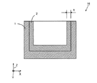
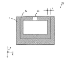
図1は本実施の形態に係る有機エレクトロルミネッセンス素子の製造方法を説明するための斜視図であり、図2は図1の坩堝の断面を示す模式図である。以下、有機エレクトロルミネッセンス素子を有機EL素子と略記する。 FIG. 1 is a perspective view for explaining a method of manufacturing an organic electroluminescence element according to the present embodiment, and FIG. 2 is a schematic view showing a cross section of the crucible of FIG. Hereinafter, the organic electroluminescence element is abbreviated as an organic EL element.
図1および図2においては、互いに直交する3方向をX方向、Y方向およびZ方向とする。X方向およびY方向は、有機層を形成する基板50の表面に平行な方向であり、Z方向は基板50の表面に垂直な方向である。
In FIG. 1 and FIG. 2, three directions orthogonal to each other are defined as an X direction, a Y direction, and a Z direction. The X direction and the Y direction are directions parallel to the surface of the
まず、坩堝10は、有機層を形成しようとする基板50の表面に対向するように配置される。図1では、基板50の下方に坩堝10が配置される。また、基板50と坩堝10との距離は100〜150mmが好ましい。
First, the
図1に示すように、坩堝10は、Y方向に延びた細長い箱型形状を有する。また、図2に示すように、坩堝10は、外層1および内層2を含む積層構造を有する。外層1および内層2のX−Z平面における断面は、コ字形状からなる。
As shown in FIG. 1, the
外層1は50W/m・K以上の熱伝導率を有する無機材料からなる。具体的に外層1の材質には、グラファイト、熱分解窒化ホウ素(PBN)、窒化アルミニウム(AlN)または炭化珪素(SiC)等が用いられる。
The
一般的にグラファイトの熱伝導率は約60W/m・Kであり、熱分解窒化ホウ素の熱伝導率は70W/m・Kであり、窒化アルミニウムの熱伝導率は約90W/m・Kであり、炭化珪素の熱伝導率は約75W/m・Kである。 Generally, graphite has a thermal conductivity of about 60 W / m · K, pyrolytic boron nitride has a thermal conductivity of 70 W / m · K, and aluminum nitride has a thermal conductivity of about 90 W / m · K. The thermal conductivity of silicon carbide is about 75 W / m · K.
また、内層2は、グラファイトを除く無機材料からなる。図2に示すように、内層2は、外層1からの熱を効率よく有機材料に伝達できるように厚みtが0.2mm以下であることが好ましい。それにより、内層2に充填された有機材料を効率よく加熱することができる。具体的に内層1の材質には、安価でかつ有機材料と反応を起こさないステンレス鋼(SUS)、ガラス、タングステン(W)、チタン(Ti)またはタンタル(Ta)等が用いられる。ガラスとしては、石英ガラス、ソーダ石灰ガラス、ホウケイ酸ガラス、鉛ガラスおよびフッ化物ガラス等が挙げられる。特に、石英ガラスを用いることが好ましい。このように、内層2を安価に作製することができる。
The
次に、基板50の表面に有機層を形成する方法について説明する。
Next, a method for forming an organic layer on the surface of the
まず、図2に示す坩堝10の内部に有機材料が充填される(図示せず)。充填される有機材料の詳細については後述する。
First, the inside of the
次いで、坩堝10に設けられたヒータ(図示せず)により坩堝10の外層1が加熱される。加熱された熱が、高い熱伝導率を有する外層1により効率よく内層2に伝達される。そして、伝達された熱が、内層2に充填された有機材料に伝達される。その伝達された熱により内層2に充填された有機材料が蒸発または昇華する。
Next, the
この際、坩堝10は、図1に示すように基板50に対して一定速度でX方向に往復移動する。移動速度は5mm/sec以上10mm/sec以下とすることが好ましい。それにより、蒸発または昇華した有機材料が基板50に均一に堆積し、基板50の表面に有機層が形成される。
At this time, the
なお、本実施の形態においては、坩堝10を基板50に対して一定速度で往復移動させることとしたが、これに限定されず、坩堝10を一方向にのみ一定速度で移動させてもよく、また、坩堝10の移動および停止を間欠的に繰り返してもよい。
In the present embodiment, the
また、ヒータとしては、外層1と接触することにより熱を伝達する直接加熱方式のヒータ、またはその他任意の方式による間接加熱方式のヒータを用いることができる。
Further, as the heater, a direct heating type heater that transfers heat by contacting the
さらに、本実施の形態においては、坩堝10の断面形状をコ字形状としたが、これに限定されず、坩堝10の断面形状には、略円形、略多角系等の任意の形状であってもよい。
Furthermore, in the present embodiment, the cross-sectional shape of the
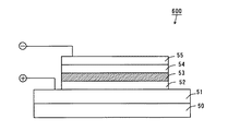
次に、図3は本実施の形態に係る製造方法により形成される有機EL素子の模式的構造図である。 Next, FIG. 3 is a schematic structural diagram of an organic EL element formed by the manufacturing method according to the present embodiment.
図3に示すように、有機EL素子600は、基板50、陽極51、ホール輸送層52、発光層53、電子輸送層54および陰極55を順に含む積層構造を有する。
As shown in FIG. 3, the
基板50上に透明な陽極51が形成される。陽極51の材料としてインジウム酸化スズ(Indium Tin Oxide:ITO)が用いられる。また、ITOの他に酸化スズ(SnO2 )または酸化インジウム(In2 O3 )等が用いられる。陽極51を覆うようにホール輸送層52が形成される。ホール輸送層52上には、発光層53が形成される。
A
ここで、ホール輸送層52の材料として、下記式(1)で示される分子構造を有するN,N'-ジ(ナフタレン-1-イル)-N,N'-ジフェニル-ベンジジン(N,N'-Di(naphthalene-1-yl)-N,N'-diphenyl-benzidine:以下、NPBと略記する)、下記式(2)で示される分子構造を有する4,4',4''-トリス(3-メチルフェニルフェニルアミノ)トリフェニルアミン(4,4',4''-tris(3-methylphenylphenylamino)triphenylamine:以下、MTDATAと略記する)、または下記式(3)で示される分子構造を有する(N,N'-ジフェニル-)N,N'-ジ(3-メチルフェニル)-1,1'-ビフェニル-4,4'-ジアミン(N,N'-diphenyl-N,N'-di(3-methylphenyl)-1,1'-biphenyl-4,4'-diamine:以下、TPDと略記する)等が用いられる。
Here, as the material of the
また、発光層53の材料として、下記式(4)で示される分子構造を有するトリス(8-ヒドロキシキノリナト)アルミニウム(Tris(8-hydroxyquinolinato)aluminum:以下、Alq3と略記する)をホスト材料として、下記式(5)で示される分子構造を有する (2-(1,1-ジメチルエチル)-6-(2-(2,3,6,7-テトラヒドロ-1,1,7,7-テトラメチル-lII,5II-ベンゾ〔ij〕キノリジン-9-イル)エテニル)-4H-ピラン-4-イリデン)プロパンジニトリル(2-(1,1-Dimethylethyl)-6-(2-(2,3,6,7-tetrahydro-1,1,7,7-tetramethyl-lII,5II-benzo〔ij〕quinolizin-9-yl)ethenyl)-4H-pyran-4-ylidene)propanedinitrile:以下、DCJTBと略記する)および下記式(6)で示される分子構造を有するルブレン(Rubrene)がドープされたもの等が用いられる。
Further, as a material of the
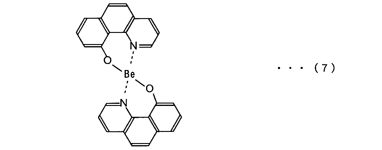
発光層53上には電子輸送層54が形成される。電子輸送層54の材料として、上記式(4)に示されるAlq3または下記式(7)に示される分子構造を有するBeBq2等のキレート金属錯体が用いられる。さらに、電子輸送層54上には、アルミニウム、リチウムを微量に含むアルミニウム合金、マグネシウムインジウム合金、マグネシウム銀合金等からなる陰極55が順に形成される。
An
図3の有機EL素子600においては、陽極51から注入されたホールと陰極55から注入された電子とが発光層53の内部で再結合することにより発光層53において光が発生し、この光が透明な陽極51を介して外部へ取り出される。
In the
上述した有機EL素子のホール輸送層52、発光層53および電子輸送層54の形成には、上記の坩堝10を用いる。
The
以上のように、本実施の形態に係る有機エレクトロルミネッセンス素子の製造方法においては、坩堝10の外層1が50W/m・K以上の高い熱伝導率を有するグラファイト、熱分解窒化ホウ素、窒化アルミニウムまたは炭化珪素等の無機材料により形成されているので、供給された熱を内層2に効率よく伝達することができる。
As described above, in the method of manufacturing the organic electroluminescence element according to the present embodiment, the
また、グラファイトはルブレン系の有機材料と反応しやすいが、内層2は安価でかつルブレン系材料と反応しないガラス、ステンレス、タングステン、チタンまたはタンタル等の無機材料により形成されているので、ヒータによる加熱温度を高くした場合でも、内層2は充填されたルブレン系の有機材料と反応しにくい。そのため、蒸着速度を低下させることなく充填された有機材料の特性の劣化を防止することができる。
In addition, graphite easily reacts with rubrene-based organic materials, but the
また、比較的安価な無機材料により内層2が構成されるので、一定期間ごとに交換が可能となり、坩堝10のメンテナンス性が向上する。
Further, since the
その結果、有機材料の特性の劣化を防止しつつ、有機エレクトロルミネッセンス素子の生産効率および量産性を向上させることができる。 As a result, it is possible to improve the production efficiency and mass productivity of the organic electroluminescence element while preventing the deterioration of the characteristics of the organic material.
なお、本実施の形態では、陽極51から光を取り出すバックエミッション構造の有機EL素子について説明したが、これに限定されず、本発明は、陰極55側から光を取り出すトップエミッション構造の有機EL素子に適用することもできる。
In the present embodiment, the back-emission structure organic EL element that extracts light from the
(坩堝の他の構成例)
次に、坩堝10の他の構成例について説明する。
(Other structural examples of crucible)
Next, another configuration example of the
図4は図1の有機EL素子の製造方法の他の例を説明するための斜視図であり、図5は図2の坩堝の断面を示す模式図である。 4 is a perspective view for explaining another example of the manufacturing method of the organic EL element of FIG. 1, and FIG. 5 is a schematic view showing a cross section of the crucible of FIG.
図4および図5においては、互いに直交する3方向をX方向、Y方向およびZ方向とする。X方向およびY方向は、有機層を形成する基板50の表面に平行な方向であり、Z方向は基板50の表面に垂直な方向である。
In FIG. 4 and FIG. 5, three directions orthogonal to each other are defined as an X direction, a Y direction, and a Z direction. The X direction and the Y direction are directions parallel to the surface of the
以下、図4および図5に示す坩堝10aが、図1および図2に示す坩堝10と異なる点について説明する。
Hereinafter, the difference between the
図4に示すように、坩堝10aは、Y方向に延びた細長い箱型形状を有する。また、図5に示すように坩堝10aは、外層1および内層2aを含む積層構造を有する。図5に示す外層1は、図1に示す外層1と同様のコ字形状を有する。一方、図5の示す内層2aは、中空部を有する箱形状からなる。内層2aの上面(Z方向側)には、所定の間隔で複数の孔11が設けられている。以上の点以外の坩堝10aの構造は、図1および図2に示す坩堝10と同様である。
As shown in FIG. 4, the
以下、実施例においては、図2に示す外層1および内層2の積層構造からなる坩堝10を複数個用いて上記図3の有機EL素子を作製した。また、比較例においては、単層構造からなる従来の坩堝を複数個用いて有機EL素子を作製した。以下、実施例および比較例の詳細について説明する。
Hereinafter, in the example, the organic EL element of FIG. 3 was manufactured using a plurality of
(実施例)
実施例において、基板50は500mm×350mmの大きさのものを用いた。坩堝10は基板50から100mm下方の位置に設けた。
(Example)
In the embodiment, the
実施例においては、グラファイトからなる外層1および厚み0.2mmのステンレス鋼からなる内層2の積層構造を有する坩堝10を複数個用いた。
In the examples, a plurality of
まず、ガラス基板50上に陽極51をスパッタ法により形成した。陽極51を形成した基板50を中性洗剤および純水で洗浄した後、所定温度下で所定時間ベークした。その後、UV/03洗浄を行い、減圧した真空蒸着装置内にセットした。続いて、グラファイトからなる単層構造の坩堝を用いてホール輸送層52としてNPBを真空蒸着により形成した。
First, the
次に、発光層53を以下に示す方法で形成した。一の積層構造の坩堝10の内部にホスト材料であるAlq3を充填し、他の積層構造の坩堝10の内部にドーパントであるDCJTBを充填し、さらに他の積層構造の坩堝10の内部にドーパントであるルブレンを充填した。そして、それらの複数の坩堝10を一定速度(10mm/sec)で一方向(X方向)に移動させつつヒータにより加熱してAlq3、DCJTBおよびルブレンを蒸発または昇華させて発光層53を形成した。
Next, the
続いて、グラファイトからなる単層構造の坩堝を用いてAlq3からなる電子輸送層54を形成した。さらに、陰極55としてアルミニウム(Al)を形成し、有機EL素子を作製した。
Subsequently, an
(比較例)
比較例においては、グラファイトからなる単層構造の坩堝を複数個用いて発光層を形成した。その他の条件は、実施例と同様にして、有機EL素子を作製した。
(Comparative example)
In the comparative example, the light emitting layer was formed using a plurality of single-layer crucibles made of graphite. Other conditions were the same as in the example, and an organic EL device was produced.
(評価)
実施例および比較例により作製した有機EL素子の発光効率、CIE(Comission International d'Eclairage )色度座標、駆動電圧、輝度半減期および分解物量を測定した。その測定結果を表1に示す。ここで、分解物量とは、有機EL素子の発光層を形成する有機材料が他の物質に変化する比率を示したものである。
(Evaluation)
Luminous efficiency, CIE (Comission International d'Eclairage) chromaticity coordinates, driving voltage, luminance half-life, and amount of decomposition products of the organic EL devices prepared in Examples and Comparative Examples were measured. The measurement results are shown in Table 1. Here, the amount of decomposition products indicates the ratio at which the organic material forming the light emitting layer of the organic EL element changes to another substance.
なお、表1においては実施例および比較例の有機EL素子の各特性の測定結果を比較例の各測定結果を1として規格化し、規格化した各測定結果を示した。 In Table 1, the measurement results of the characteristics of the organic EL elements of Examples and Comparative Examples were normalized with each measurement result of the Comparative Example as 1, and each measurement result normalized was shown.
なお、xはCIE色度座標の横軸を示し、yはCIE色度座標の縦軸を示す。 Note that x indicates the horizontal axis of the CIE chromaticity coordinates, and y indicates the vertical axis of the CIE chromaticity coordinates.
表1に示すように、実施例および比較例で作製した有機EL素子のCIE色度座標については、相違がなかった。 As shown in Table 1, there was no difference in CIE chromaticity coordinates of the organic EL elements produced in the examples and comparative examples.
一方、実施例で作製した有機EL素子の発光効率は比較例で作製した有機EL素子の発光効率の1.48倍となった。 On the other hand, the luminous efficiency of the organic EL device produced in the example was 1.48 times that of the organic EL device produced in the comparative example.
実施例で作製した有機EL素子の駆動電圧は比較例で作製した有機EL素子の駆動電圧の0.98倍となった。 The driving voltage of the organic EL element produced in the example was 0.98 times the driving voltage of the organic EL element produced in the comparative example.
また、実施例で作製した有機EL素子の輝度半減期は、比較例で作製した有機EL素子の輝度半減期の1.3倍となった。 Moreover, the luminance half-life of the organic EL element produced in the Example became 1.3 times the luminance half-life of the organic EL element produced in the comparative example.
さらに、実施例で作製した有機EL素子の分解物量は比較例で作製した有機EL素子の分解物量の0.66倍となった。 Furthermore, the decomposition amount of the organic EL element produced in the example was 0.66 times the decomposition amount of the organic EL element produced in the comparative example.
以上のことにより、単層構造からなる坩堝を用いた場合には、有機材料が坩堝の材質と反応して劣化するのに対し、積層構造からなる坩堝10を用いた場合には、ルブレン系の有機材料の劣化を防止することができ、発光効率、輝度半減期および分解物量を向上させることができる。さらに、外層1が高い熱伝導率を有するため、蒸着速度を下げることなく、効率よく有機EL素子を生産することができる。
As described above, when a crucible having a single-layer structure is used, an organic material is deteriorated by reacting with the material of the crucible, whereas when using a
本発明は、有機エレクトロルミネッセンス素子の製造方法に用いることができる。 The present invention can be used in a method for producing an organic electroluminescence element.
1 外層
2,2a 内層
10,10a 坩堝
50 基板
51 陽極
52 ホール輸送層
53 発光層
54 電子輸送層
55 陰極
1
Claims (6)
外層および内層を含む積層構造を有する坩堝内に前記有機材料を充填する工程と、
前記坩堝を加熱することにより前記基板上に前記有機材料からなる有機層を形成する工程とを備え、
前記坩堝の外層は前記内層よりも高い熱伝導率を有する第1の無機材料により形成され、前記内層はグラファイトを除く第2の無機材料により形成されたことを特徴する有機エレクトロルミネッセンス素子の製造方法。 A method for producing an organic electroluminescence device comprising an organic layer made of an organic material on a substrate,
Filling the organic material in a crucible having a laminated structure including an outer layer and an inner layer;
Forming an organic layer made of the organic material on the substrate by heating the crucible,
The outer layer of the crucible is formed of a first inorganic material having a higher thermal conductivity than the inner layer, and the inner layer is formed of a second inorganic material excluding graphite. .
Priority Applications (1)
| Application Number | Priority Date | Filing Date | Title |
|---|---|---|---|
| JP2004105815A JP2005293969A (en) | 2004-03-31 | 2004-03-31 | Manufacturing method of organic electroluminescent element |
Applications Claiming Priority (1)
| Application Number | Priority Date | Filing Date | Title |
|---|---|---|---|
| JP2004105815A JP2005293969A (en) | 2004-03-31 | 2004-03-31 | Manufacturing method of organic electroluminescent element |
Publications (1)
| Publication Number | Publication Date |
|---|---|
| JP2005293969A true JP2005293969A (en) | 2005-10-20 |
Family
ID=35326685
Family Applications (1)
| Application Number | Title | Priority Date | Filing Date |
|---|---|---|---|
| JP2004105815A Withdrawn JP2005293969A (en) | 2004-03-31 | 2004-03-31 | Manufacturing method of organic electroluminescent element |
Country Status (1)
| Country | Link |
|---|---|
| JP (1) | JP2005293969A (en) |
Cited By (1)
| Publication number | Priority date | Publication date | Assignee | Title |
|---|---|---|---|---|
| US7922820B2 (en) * | 2004-11-05 | 2011-04-12 | Samsung Mobile Display Co., Ltd. | Heating crucible and deposition apparatus including the same |
-
2004
- 2004-03-31 JP JP2004105815A patent/JP2005293969A/en not_active Withdrawn
Cited By (1)
| Publication number | Priority date | Publication date | Assignee | Title |
|---|---|---|---|---|
| US7922820B2 (en) * | 2004-11-05 | 2011-04-12 | Samsung Mobile Display Co., Ltd. | Heating crucible and deposition apparatus including the same |
Similar Documents
| Publication | Publication Date | Title |
|---|---|---|
| CN100580976C (en) | Organic light emitting display, cathode composite layer and method of manufacturing the same | |
| JP2005293968A (en) | Manufacturing method of organic electroluminescent element | |
| TWI293211B (en) | Organic electroluminescent device and method of manufacturing the same | |
| JP2003059668A (en) | Organic light-emitting device | |
| JPWO1998051757A1 (en) | organic electroluminescence element | |
| JP2004288619A (en) | High efficiency organic electroluminescent device | |
| KR20090095022A (en) | White organic light emitting device | |
| CN101656264A (en) | Organic light emitting display | |
| JP2003059644A (en) | Electroluminescent device | |
| WO2011074633A1 (en) | Organic electroluminescent element | |
| CN1501753A (en) | Organic electroluminescence display device and manufacturing method thereof | |
| JP2007281454A (en) | Image display system containing electroluminescent element, and method for manufacturing same | |
| JP2001155862A (en) | Light emitting device and manufacturing method thereof | |
| JP6280234B2 (en) | Organic electroluminescent device and production method thereof | |
| JP2003303691A (en) | Organic electronic light emitting device | |
| WO2009021365A1 (en) | Oled and method thereof | |
| CN103688347B (en) | Thin Film Encapsulation of Organic Light Emitting Diodes | |
| JP3877613B2 (en) | Method for manufacturing organic electroluminescence display device | |
| JP4837774B2 (en) | Organic light emitting device manufacturing method and organic light emitting device manufactured thereby | |
| KR20040068000A (en) | Using compacted organic materials in making white light emitting oleds | |
| JP2011504536A (en) | High efficiency aromatic electroluminescent compound and electroluminescent device using the same | |
| KR100236011B1 (en) | Organic electroluminescence device and method for fabricating the same | |
| JP2000012237A (en) | Manufacturing method of organic electroluminescent display device | |
| CN106374048B (en) | Organic light emitting element | |
| JP2005293969A (en) | Manufacturing method of organic electroluminescent element |
Legal Events
| Date | Code | Title | Description |
|---|---|---|---|
| A621 | Written request for application examination |
Free format text: JAPANESE INTERMEDIATE CODE: A621 Effective date: 20060725 |
|
| A761 | Written withdrawal of application |
Free format text: JAPANESE INTERMEDIATE CODE: A761 Effective date: 20090427 |