JP2005293886A - Switch contact plate manufacturing method and switch board manufacturing method - Google Patents
Switch contact plate manufacturing method and switch board manufacturing method Download PDFInfo
- Publication number
- JP2005293886A JP2005293886A JP2004103359A JP2004103359A JP2005293886A JP 2005293886 A JP2005293886 A JP 2005293886A JP 2004103359 A JP2004103359 A JP 2004103359A JP 2004103359 A JP2004103359 A JP 2004103359A JP 2005293886 A JP2005293886 A JP 2005293886A
- Authority
- JP
- Japan
- Prior art keywords
- switch contact
- switch
- contact
- plate
- exposed
- Prior art date
- Legal status (The legal status is an assumption and is not a legal conclusion. Google has not performed a legal analysis and makes no representation as to the accuracy of the status listed.)
- Granted
Links
- 238000004519 manufacturing process Methods 0.000 title claims abstract description 35
- 239000011347 resin Substances 0.000 claims abstract description 40
- 229920005989 resin Polymers 0.000 claims abstract description 40
- 238000000034 method Methods 0.000 claims abstract description 34
- 238000004080 punching Methods 0.000 claims abstract description 32
- 239000002184 metal Substances 0.000 claims abstract description 20
- 238000000465 moulding Methods 0.000 claims description 37
- 239000000758 substrate Substances 0.000 description 17
- 238000010586 diagram Methods 0.000 description 10
- 238000003825 pressing Methods 0.000 description 10
- 238000007665 sagging Methods 0.000 description 6
- 238000003860 storage Methods 0.000 description 6
- 230000002950 deficient Effects 0.000 description 3
- 230000002093 peripheral effect Effects 0.000 description 3
- 238000013459 approach Methods 0.000 description 2
- 238000005520 cutting process Methods 0.000 description 2
- 230000000694 effects Effects 0.000 description 2
- 239000000463 material Substances 0.000 description 2
- 229910001369 Brass Inorganic materials 0.000 description 1
- 230000001154 acute effect Effects 0.000 description 1
- 239000010951 brass Substances 0.000 description 1
- 230000008878 coupling Effects 0.000 description 1
- 238000010168 coupling process Methods 0.000 description 1
- 238000005859 coupling reaction Methods 0.000 description 1
- 239000000155 melt Substances 0.000 description 1
- 238000012986 modification Methods 0.000 description 1
- 230000004048 modification Effects 0.000 description 1
Images


Landscapes
- Manufacture Of Switches (AREA)
- Rotary Switch, Piano Key Switch, And Lever Switch (AREA)
Abstract
【課題】バリによって摺動子が損傷することなく、また設計どおりのオンオフ波形が得られるスイッチ接点板の製造方法及びスイッチ基板の製造方法を提供する。
【解決手段】スイッチ接点A1,A2を有し、モールド樹脂製のケース内に前記スイッチ接点A1,A2の表面が露出するように埋め込まれるスイッチ接点板20の製造方法である。金属板をプレス金型によって打抜くことでスイッチ接点A1,A2を有するスイッチ接点板20を取り出す打抜き工程と、打抜きによって形成されたスイッチ接点板20のスイッチ接点A1,A2の部分の面をダイ300とポンチ350によって押し潰すスイッチ接点押し潰し工程と、を具備する。
【選択図】図3Provided are a method for manufacturing a switch contact plate and a method for manufacturing a switch board, in which a slider is not damaged by burrs and an on / off waveform as designed can be obtained.
A method of manufacturing a switch contact plate 20 having switch contacts A1 and A2 and embedded in a molded resin case so that the surfaces of the switch contacts A1 and A2 are exposed. A punching process of taking out the switch contact plate 20 having the switch contacts A1 and A2 by punching a metal plate with a press die, and the surface of the switch contact A1 and A2 portion of the switch contact plate 20 formed by punching are formed on the die 300. And a switch contact crushing step of crushing with the punch 350.
[Selection] Figure 3
Description
本発明は、モールド樹脂製のケース内に埋め込まれて使用されるスイッチ接点板の製造方法及びスイッチ基板の製造方法に関するものである。 The present invention relates to a method for manufacturing a switch contact plate and a method for manufacturing a switch substrate, which are used by being embedded in a case made of molded resin.
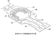
従来、回転型スイッチ基板の中には、図16に示すように、一枚の金属板をプレス加工することによってスイッチ接点a1,a2及びコモン接点a5と、三本の端子板81とを一体に形成してなるスイッチ接点板80を形成し、このスイッチ接点板80を上下の成形金型で挟持してその内部のキャビティーにモールド樹脂を成形することで、図17に示すようにケース85を形成し、その後リードフレーム87,89の部分を切り離すことで製造されるケース付きのスイッチ基板90がある。
Conventionally, in a rotary type switch board, as shown in FIG. 16, the switch contacts a1 and a2 and the common contact a5 and the three
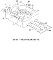
このスイッチ基板90はケース85の中央に図示しない摺動子を固定した摺動型物を収納する凹状の収納部91を有し、この収納部91の底面に前記スイッチ接点a1,a2及びコモン接点a5の表面を露出して構成されている。
The
そして前記収納部91内に収納した摺動子の摺動接点が回転中心点Oを中心とする一点鎖線で示される二つの円周上(スイッチ接点a1,a2及びコモン接点a3上)を回転摺動することにより、前記スイッチ接点a1,a2で三本の端子板81間のオンオフ状態が変化する。
Then, the sliding contact of the slider housed in the
ところで上記スイッチ接点板80は金属板をプレス金型によってスイッチ接点板80の外形形状に打抜くことによって製造される。
By the way, the
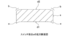
ここで図18は以上のようにプレス加工によって製造されたスイッチ接点板80の一つのスイッチ接点a(a1,a2の何れか一つ)を、摺動子が摺動する方向に向けて切断した拡大断面図である。プレス加工は金属板を載せた固定側プレス金型の上から移動側プレス金型を押し付けることで行われるため、同図に示すように、移動側プレス金型を押し付けた側のスイッチ接点aの外周辺にはダレ面bが生じ、スイッチ接点aの反対面側の外周辺にはバリeが生じる。
Here, in FIG. 18, one switch contact a (any one of a1 and a2) of the
そしてスイッチ接点aの摺動子が摺動する面、即ち前記図16に示すケース85の収納部91内に露出する露出面として、前記バリeの生じている側の面d1を用いると、その上を摺動する摺動子の摺動接点がこのバリeに引っかかることで、摺動接点に損傷が生じてしまうという問題があった。
When the surface d1 on the side where the burr e is generated is used as a surface on which the slider of the switch contact a slides, that is, an exposed surface exposed in the
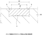
一方スイッチ接点aのダレ面bのある側の面を摺動子が摺動する露出面d2とすると、上記摺動接点が損傷するという問題は生じないが、その代わりに以下のような問題が生じる。即ちこのスイッチ接点aの周囲にモールド樹脂製のケース85を成形する際は、露出面d2の表面を成形金型の表面に当接することとなるが、その際成形金型の表面とダレ面bの間に微細な隙間が生じる。このため成形樹脂を成形金型内に充填する際に、この隙間に成形樹脂が流れ込み、その結果、図19に示すように、ダレ面bの上が成形樹脂によって覆われ、露出面d2の幅k1がスイッチ接点aの幅k2よりも狭くなり、設計どおりのオンオフ波形が得られなくなってしまう(オンしている間隔が短くなってしまう)。また左右のダレ面bの幅寸法には誤差が大きくて摺動によるオンオフポイントが変化し、この点からもオンオフ波形に歪が生じていた。
本発明は上述の点に鑑みてなされたものでありその目的は、バリによって摺動子が損傷することなく、また設計どおりのオンオフ波形が得られるスイッチ接点板の製造方法及びスイッチ基板の製造方法を提供することにある。 SUMMARY OF THE INVENTION The present invention has been made in view of the above-described points, and an object of the present invention is to produce a switch contact plate and a switch substrate that do not damage the slider due to burrs and can obtain an on-off waveform as designed. Is to provide.
本願請求項1に記載の発明は、スイッチ接点を有し、モールド樹脂製のケース内に前記スイッチ接点の表面が露出するように埋め込まれるスイッチ接点板の製造方法において、金属板をプレス金型によって打抜くことで前記スイッチ接点を有するスイッチ接点板を取り出す打抜き工程と、前記打抜きによって形成されたスイッチ接点板の少なくともスイッチ接点の面を押し潰すスイッチ接点押し潰し工程と、を具備することを特徴とするスイッチ接点板の製造方法にある。 The invention according to claim 1 of the present application is a method of manufacturing a switch contact plate that has a switch contact and is embedded in a case made of molded resin so that the surface of the switch contact is exposed. A punching step of taking out a switch contact plate having the switch contact by punching, and a switch contact crushing step of crushing at least a surface of the switch contact of the switch contact plate formed by the punching. A switch contact plate manufacturing method.
本願請求項2に記載の発明は、前記スイッチ接点押し潰し工程において、前記スイッチ接点の面は、スイッチ接点の露出面の反対面側から押し潰されることを特徴とする請求項1に記載のスイッチ接点板の製造方法にある。 The invention according to claim 2 is characterized in that, in the switch contact crushing step, the surface of the switch contact is crushed from the opposite side of the exposed surface of the switch contact. It is in the manufacturing method of a contact plate.
本願請求項3に記載の発明は、前記スイッチ接点押し潰し工程において、前記スイッチ接点の面をこのスイッチ接点の露出面の反対面側から押し潰す際は、このスイッチ接点の露出面を露出面側に突出させることを特徴とする請求項2に記載のスイッチ接点板の製造方法にある。 According to the third aspect of the present invention, in the switch contact crushing step, when the surface of the switch contact is crushed from the side opposite to the exposed surface of the switch contact, the exposed surface of the switch contact is exposed side. 3. The method of manufacturing a switch contact plate according to claim 2, wherein
本願請求項4に記載の発明は、金属板をプレス金型によって打抜くことでスイッチ接点を有するスイッチ接点板を取り出す打抜き工程と、前記打抜きによって形成されたスイッチ接点板の少なくともスイッチ接点の面を押し潰すスイッチ接点押し潰し工程と、前記スイッチ接点板をモールド樹脂製のケース内に前記スイッチ接点の一方の表面が露出するように埋め込むケース成形工程と、を具備することを特徴とするスイッチ基板の製造方法にある。 In the invention according to claim 4 of the present invention, a punching step of taking out a switch contact plate having a switch contact by punching a metal plate with a press die, and at least a surface of the switch contact of the switch contact plate formed by the punching is provided. A switch contact crushing step of crushing, and a case molding step of embedding the switch contact plate in a molded resin case so that one surface of the switch contact is exposed. In the manufacturing method.
本願請求項5に記載の発明は、前記スイッチ接点の面は、スイッチ接点の露出面の反対面側から押し潰されることを特徴とする請求項4に記載のスイッチ基板の製造方法にある。 The invention according to claim 5 of the present application is the method for manufacturing a switch board according to claim 4, wherein the surface of the switch contact is crushed from the opposite side of the exposed surface of the switch contact.
請求項1に記載の発明によれば、打抜きによって形成されたスイッチ接点板のスイッチ接点の面を押し潰して平面状にしたので、打抜きによって生じたバリ及びダレ面が修正される。従ってバリ側の面を露出面とした場合はその上を摺動する摺動子の摺動接点に損傷が生じることはなくなり、またダレ面側を露出面とした場合はモールド樹脂製のケース内にスイッチ接点を埋め込んだ際にダレ面上を覆うモールド樹脂の幅が小さくなってケース表面に露出するスイッチ接点の露出面の幅が正規のスイッチ接点の幅に近づき、設計に近いオンオフ波形が得られるようになる。 According to the first aspect of the present invention, since the surface of the switch contact of the switch contact plate formed by punching is crushed and flattened, the burrs and sagging surfaces generated by punching are corrected. Therefore, if the burr-side surface is an exposed surface, the sliding contact of the slider that slides on it will not be damaged, and if the sag surface side is an exposed surface, it will not be damaged in the mold resin case. When the switch contact is embedded in the mold, the width of the mold resin that covers the sag surface becomes smaller, and the width of the exposed surface of the switch contact exposed on the case surface approaches the width of the regular switch contact, and an on-off waveform close to the design is obtained. Be able to.
請求項2に記載の発明によれば、スイッチ接点の面を、スイッチ接点の露出面の反対面側から押し潰したので、露出面はスイッチ接点板のスイッチ接点の周囲の部分の表面と同一高さに位置し、このため前記露出面やその周囲の表面を成形金型の当接面に当接してその反対の面側に成形樹脂を成形することで露出面やその周囲の表面を露出した状態でケースを取り付ける場合に、前記露出面をその周囲の表面と同じ圧接力で成形金型の当接面に当接でき、従って露出面の上面側に成形樹脂が入り込むことはなく、スイッチ接点の全面が露出面としてケースの表面に露出し、設計通りのオンオフ波形が得られるようになる。 According to the second aspect of the present invention, since the surface of the switch contact is crushed from the side opposite to the exposed surface of the switch contact, the exposed surface is flush with the surface of the portion around the switch contact of the switch contact plate. Therefore, the exposed surface and the surrounding surface are exposed by abutting the exposed surface and the surrounding surface to the abutting surface of the molding die and molding a molding resin on the opposite surface side. When mounting the case in a state, the exposed surface can be brought into contact with the contact surface of the molding die with the same pressure contact force as the surrounding surface, so that the molding resin does not enter the upper surface side of the exposed surface, and the switch contact Is exposed on the surface of the case as an exposed surface, and an on / off waveform as designed can be obtained.
請求項3に記載の発明によれば、スイッチ接点の面をスイッチ接点の露出面の反対面側から押し潰す際に、スイッチ接点の露出面を露出面側に突出させることとしたので、露出面はスイッチ接点板のスイッチ接点の周囲の部分の表面よりもその表面側に少し突出し、このため前記露出面やその周囲の表面を成形金型の当接面に当接してその反対の面側に成形樹脂を成形することで露出面やその周囲の表面を露出した状態でケースを取り付ける場合に、前記露出面をその周囲の表面よりも強い圧接力で成形金型の当接面に当接でき、従って露出面の上面側に成形樹脂が入り込むことはなく、スイッチ接点の全面が露出面としてケースの表面に露出し、設計通りのオンオフ波形が得られるようになる。 According to the third aspect of the present invention, when the surface of the switch contact is crushed from the opposite surface side of the exposed surface of the switch contact, the exposed surface of the switch contact is projected to the exposed surface side. Protrudes slightly to the surface side of the switch contact plate surrounding the switch contact, so that the exposed surface and the surrounding surface are in contact with the contact surface of the molding die and on the opposite surface side. When mounting the case with the exposed surface and its surrounding surface exposed by molding resin, the exposed surface can be brought into contact with the contact surface of the molding die with a stronger pressing force than the surrounding surface. Therefore, the molding resin does not enter the upper surface side of the exposed surface, and the entire surface of the switch contact is exposed as an exposed surface on the surface of the case, and an on / off waveform as designed can be obtained.
請求項4に記載の発明によれば、打抜きによって形成されたスイッチ接点板の少なくともスイッチ接点の面を押し潰すことで、打抜きによって生じたバリ及びダレ面を修正してスイッチ接点の表面全体を平面状にした上で、このスイッチ接点板をモールド樹脂製のケース内にスイッチ接点の一方の表面が露出するように埋め込むので、バリ側の面を露出面とした場合はその上を摺動する摺動子の摺動接点に損傷が生じることはなくなり、またダレ面側を露出面とした場合はケース内に埋め込んだスイッチ接点の露出面の幅が正規のスイッチ接点の幅に近づき、設計に近いオンオフ波形が得られるようになる。 According to the fourth aspect of the present invention, by crushing at least the surface of the switch contact of the switch contact plate formed by punching, the burrs and sag surfaces generated by the punching are corrected to make the entire surface of the switch contact flat. Then, the switch contact plate is embedded in the molded resin case so that one surface of the switch contact is exposed. If the burr side surface is an exposed surface, the sliding surface slides on it. The sliding contact of the moving element will not be damaged, and if the sag surface side is exposed, the exposed surface width of the switch contact embedded in the case will approach the width of the normal switch contact, which is close to the design. An on / off waveform can be obtained.
請求項5に記載の発明によれば、スイッチ接点の面を、スイッチ接点の露出面の反対面側から押し潰したので、スイッチ接点の露出面はスイッチ接点板のスイッチ接点の周囲の部分の表面と同一高さに位置し、このため前記露出面やその周囲の表面を成形金型の当接面に当接してその反対の面側に成形樹脂を成形することで露出面やその周囲の表面を露出した状態でケースを取り付けるケース成形工程において、前記露出面をその周囲の表面と同じ圧接力で成形金型の当接面に当接でき、従って成形金型内に成形樹脂を圧入する際、露出面の上面側に成形樹脂が入り込むことはなく、スイッチ接点の全面が露出面としてケースの表面に確実に露出する。 According to the invention described in claim 5, since the surface of the switch contact is crushed from the opposite side of the exposed surface of the switch contact, the exposed surface of the switch contact is the surface of the portion around the switch contact of the switch contact plate. Therefore, the exposed surface and the surrounding surface are formed by abutting the exposed surface and the surrounding surface with the abutting surface of the molding die and molding a molding resin on the opposite surface side. In the case molding process in which the case is mounted with the case exposed, the exposed surface can be brought into contact with the contact surface of the molding die with the same pressure contact force as the surrounding surface, and therefore when the molding resin is pressed into the molding die. The molding resin does not enter the upper surface side of the exposed surface, and the entire surface of the switch contact is reliably exposed on the surface of the case as the exposed surface.
以下、本発明の実施形態を図面に基づいて詳細に説明する。
〔第一実施形態〕
図1乃至図8は、本実施形態にかかるスイッチ接点板20の製造方法及びこのスイッチ接点板20を用いたスイッチ基板(ケース付きスイッチ基板)10の製造方法を示す図である。以下、工程順にこれらの製造方法を説明する。
Hereinafter, embodiments of the present invention will be described in detail with reference to the drawings.
[First embodiment]
1 to 8 are views showing a method for manufacturing the
1.打抜き工程
スイッチ接点板20及びスイッチ基板10を製造するには、まず図1に示すように薄い平板状の金属板3を用意する。金属板3としては例えば黄銅板を用い、その厚みが0.1mmのものを使用する。そしてこの金属板3を図示しない固定側のプレス金型の上に載置し、その反対側の面(即ち上側)から図示しない可動側のプレス金型を押し付けて、金属板3を打ち抜き加工(プレス加工)し、これによって図2に示すようなスイッチ接点A(A1,A2,A3)を有するスイッチ接点板20の外形形状を打ち抜く。
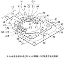
1. Punching process In order to manufacture the
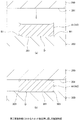
ここでスイッチ接点板20は図2に示すように、その内側に二つの円弧状のスイッチ接点部G1,G2を形成し、その外側の円周上にコモンとなる円弧状のコモン接点A3を形成している。さらに詳細に説明すれば、スイッチ接点部G1,G2はそれぞれ二本の円弧状の連結部E1,E2,E3,E4と、連結部E1と連結部E2間、連結部E3と連結部E4間を半径方向に連結する複数の帯状のスイッチ接点A1,A2で構成されている。なおスイッチ接点A1,A2は、開口部F1,F2を介して(但しスイッチ接点部G1,G2の終端側には開口部はない)形成されている。そして外周側の連結部E2,E4はその外周に設置した円弧状の支持部材H1,H2に、接続片J1,J2によって接続されている。
Here, as shown in FIG. 2, the
一方スイッチ接点A1を設けた側の金属板にはさらに端子当接部23を設け、スイッチ接点A2を設けた側の金属板にはさらに端子当接部25を設け、コモン接点A3を設けた金属板にはさらに端子当接部27を設けている。端子当接部27は端子当接部23,25に連結部31によって連結されている。なお端子当接部23,25にはそれぞれ下記する端子板40の係止突起41を挿入する固定穴33,35とスイッチ接点板20の位置決め用のピンを挿入する穴37,39とが設けられている。また端子当接部27には端子板40の係止突起41を挿入する固定穴38が設けられている。
On the other hand, the metal plate on the side where the switch contact A1 is provided is further provided with a
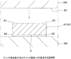
2.スイッチ接点押し潰し工程
次に以上のようにして形成されたスイッチ接点板20を、図3に示すように、表面が平面状のダイ300の上に載置し、その上から前記スイッチ接点A1,A2の部分を押し潰すように、ポンチ350を押し付ける。ポンチ350は円筒状に形成されることでその先端面351がリング状で平面状に形成されており、ちょうどこの先端面351は前記スイッチ接点A1,A2の部分のみに当接する寸法形状に形成されている。即ちリング状の先端面351の各部の半径方向の幅は、スイッチ接点A1,A2の半径方向の幅(連結部E1,E2,E3,E4を含まない幅)と同一に形成されている。
2. Switch Contact Crushing Step Next, the
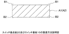
図4はダイ300の上に載置されるスイッチ接点A1(A2)の部分を、図3のL線の如く、摺動子が摺動する方向に沿って切断した拡大断面図である。同図に示すようにスイッチ接点A1(A2)の一方の面(この図では上側の面)の前記プレス加工によって切断された外周辺は下方向に向かって徐々に湾曲して傾斜するダレ面B1となっており、もう一方の面(摺動子が摺動する露出面Dとなる面)(この図では下側の面)の前記プレス加工によって切断された外周辺は下方向に向かって徐々に湾曲して傾斜しその先端が鋭角となるバリB2となっている。即ちダレ面B1とバリB2は、金属板3を可動金型と固定金型で挟持してプレスカットすることによって形成されるものである。
FIG. 4 is an enlarged cross-sectional view of a portion of the switch contact A1 (A2) placed on the
そしてこの実施形態においては、露出面DとなるバリB2が突出している側の面をダイ300の上に載置し、ダレ面B1側の面にポンチ350を押し付け、これによってスイッチ接点A1(A2)の部分を厚み方向に押し潰すこととしている。
In this embodiment, the surface on which the burr B2 that becomes the exposed surface D protrudes is placed on the
以上のようにスイッチ接点A1,A2の部分をダイ300とポンチ350によって押し潰せば、図5に示すようにスイッチ接点A1(A2)は全体として少し厚みを薄くしながら、同時にダレ面B1とバリB2の部分も平面状になるように成形され、従ってダレ面B1は小さくなり、バリB2は潰される。
As described above, when the switch contacts A1 and A2 are crushed by the
3.端子板取付工程
次に以上のようにしてスイッチ接点A1,A2の表面形状を修正されたスイッチ接点板20は、図6に示すように、その端子当接部23,25,27上に三枚の端子板40の一端を当接して各端子板40に設けた係止突起41を固定穴33,35,38(図2参照)に挿入し、各係止突起41の各固定穴33,35,38の裏面側に突出した部分をカシメて機械的に固定する。このときスイッチ接点板20の端子板40を固定する側の面は、この実施形態では、前記スイッチ接点A1,A2等のバリB2が生じている側の面とする。
3. Terminal plate attachment process Next, three
4.ケース成形工程
次に図7に示すように前記端子板40を取り付けたスイッチ接点板20の上下面を第一,第二金型M1,M2によって挟持する。第一,第二金型M1,M2には後にケースとなるキャビティーC1,C2が設けられている。図7に示すように第一金型M1のリング状のキャビティーC1の中央にはスイッチ接点板20の各スイッチ接点A1,A2及びコモン接点A3の露出面Dとなる表面を当接する平面状の当接面M13が設けられている。また第二金型M2の当接面M13に対向する面からはスイッチ接点板20の下面各部を当接面M13に向けて押し付ける多数のピンM25が設けられている。またキャビティーC2にはゲートP1が接続されている。スイッチ接点板20と端子板40の重ね合わされた部分の端子板40の先端部分45は、第一金型M1に設けた押圧部M11と第二金型M2に設けた押圧部M21とによって挟持されている。
4). Case Forming Step Next, as shown in FIG. 7, the upper and lower surfaces of the
そしてこの実施形態において、第一金型M1の当接面M13に当接する前記スイッチ接点A1,A2等の面は、バリB2が生じている側の面(この面が露出面Dとなる)としている。 In this embodiment, the surfaces of the switch contacts A1, A2, etc. that abut on the abutment surface M13 of the first mold M1 are the surfaces on which the burr B2 is generated (this surface becomes the exposed surface D). Yes.
そしてゲートP1から溶融モールド樹脂を圧入すると、キャビティーC1,C2内に溶融モールド樹脂が満たされる。そして充填した溶融モールド樹脂が固化した後に第一,第二金型M1,M2を取り外せば、図8に示すように端子板40を固定したスイッチ接点板20にケース50を取り付けたものが得られる。ここで第一金型M1の当接面M13に当接していたスイッチ接点板20の各スイッチ接点A1,A2及びコモン接点A3の表面は、ケース50の凹状の収納部51の底面に収納部51の底面と同一面で露出する。各スイッチ接点A1,A2及びコモン接点A3の露出面Dは、バリB2が生じている側の面である。
When the molten mold resin is press-fitted from the gate P1, the cavities C1 and C2 are filled with the molten mold resin. If the first and second molds M1 and M2 are removed after the filled molten mold resin is solidified, a case in which the
そしてリードフレーム15,45と連結部31の部分とを切断して除去すれば、図9に示すスイッチ基板10が完成する。
Then, if the lead frames 15 and 45 and the connecting
図10は以上のようにして製造されたスイッチ基板10中の一つのスイッチ接点A1(A2)の部分(図5と同一部分)を摺動子が摺動する方向に沿って切断した拡大断面図である。前述のようにスイッチ接点板20を第一金型M1と第二金型M2によって挟持した際、スイッチ接点A1(A2)のバリB2が生じている側の面を当接面M13に当接したので、図10に示すように、このスイッチ接点A1(A2)のバリB2が生じている側の面がケース50の収納部51の底面への露出面Dとなる。
FIG. 10 is an enlarged cross-sectional view in which one switch contact A1 (A2) portion (the same portion as FIG. 5) in the
そしてこの実施形態の場合、図10に示すように、バリB2は潰されて小さくなっているので、露出面Dはその全体が略平面状になる。従ってその上を摺動子の摺動接点が摺動しても摺動接点が損傷することはなく、また設計通りのオンオフ波形が得られる。 In the case of this embodiment, as shown in FIG. 10, since the burr B2 is crushed and reduced in size, the entire exposed surface D is substantially flat. Therefore, even if the sliding contact of the slider slides thereon, the sliding contact is not damaged, and an on-off waveform as designed can be obtained.
なおこの実施形態において、ダイ300とポンチ350によって、スイッチ接点板20全体(端子当接部23,25,27や連結部31やリードフレーム15等を含むスイッチ接点板20全体)を押し潰さず、スイッチ接点A1,A2の部分のみを押し潰したのは、以下の理由による。即ちもしスイッチ接点板20全体を押し潰すとすると、強力なプレス圧力が必要となって、大型のプレス機が必要となり、コストが上昇して現実的でない。またスイッチ接点板20全体を押し潰すこととすると、押し潰したくない部分、例えば位置決め用のピンを挿入する穴37,39も潰れる恐れが生じ、これが潰れると位置決め用のピンが挿入できなくなるというような問題が生じる。そこでこの実施形態では、スイッチ接点A1,A2の部分のみを押し潰すこととしたのである。なおこの実施形態ではスイッチ接点A1,A2の部分のみを押し潰したが、その周囲の連結部E1,E2,E3,E4の部分を含めたスイッチ接点部G1,G2の部分全体のみを押し潰すようにしても良い。またコモン接点A3の部分も合わせて押し潰しても良い。
In this embodiment, the
またこの実施形態においては、スイッチ接点A1,A2の面を、スイッチ接点A1,A2の露出面Dの反対面側から押し潰している。即ち前記スイッチ接点押し潰し工程において、スイッチ接点A1,A2のケース50からの露出面Dとなる側(即ちバリB2が生じている面側)にダイ300を配置した状態でその反対側の面からポンチ250を押し付けることで、露出面Dとなる面の反対面側からスイッチ接点A1,A2の面を押し潰すようにしている。このように構成したのは以下の理由による。
In this embodiment, the surfaces of the switch contacts A1 and A2 are crushed from the side opposite to the exposed surface D of the switch contacts A1 and A2. That is, in the switch contact crushing step, the switch contacts A1 and A2 from the opposite surface in a state where the
即ちもしスイッチ接点A1,A2の面を、スイッチ接点A1,A2の露出面Dの側から押し潰すこととすると、露出面D側が押し潰され、露出面Dはスイッチ接点板20の露出面D側の他の面よりも下がった位置に位置してしまうからである。ここで図11(a),(b)は押し潰し工程後のスイッチ接点板20を図2に示すK−K線の部分で切断した断面拡大図であり、図11(a)は露出面D側からポンチ350によって押し潰した場合を示し、図11(b)は露出面Dの反対側の面からポンチ350によって押し潰した場合(即ちこの実施形態の場合)を示している。なお説明の都合上、その厚みは実際よりもかなり厚く記載している。図11(a)に示すように、露出面D側からスイッチ接点A1をポンチ350によって押し潰した場合は、露出面Dがそれ以外のスイッチ接点板20の露出面D側の面(連結部E1,E2や支持部材H1やリードフレーム15等の面)よりも凹んでしまう。このためこの露出面D側を図7に示すように第一金型M1の平面状の当接面M13に当接した場合、露出面Dと当接面M13の間は密着せず全体に僅かな隙間が生じてしまう。そしてこの状態でキャビティーC1,C2内に溶融成形樹脂を圧入すると、前記露出面Dと当接面M13の間の隙間に成形樹脂が入り込む恐れがあり、もし成形樹脂が入り込んだ場合は露出面Dの上面が成形樹脂によって覆われ、不良品となってしまう恐れがある。
That is, if the surfaces of the switch contacts A1 and A2 are crushed from the exposed surface D side of the switch contacts A1 and A2, the exposed surface D side is crushed, and the exposed surface D is the exposed surface D side of the
これに対して図11(b)に示すように、露出面Dの反対面側からスイッチ接点A1をポンチ350によって押し潰した場合は、露出面Dがそれ以外のスイッチ接点板20の露出面D側の面(連結部E1,E2や支持部材H1やリードフレーム15等の面)と同一面を維持する。このためこの露出面D側を図7に示すように第一金型M1の平面状の当接面M13に当接した場合、露出面Dと当接面M13の間は密着する(この実施形態の場合は少なくとも周囲のバリB2を設けた外周辺が当接面M13に密着する)。そしてこの状態でキャビティーC1,C2内に溶融成形樹脂を圧入しても、前記露出面Dと当接面M13の間に成形樹脂が入り込むことはなく、不良品が生じることはない。
On the other hand, as shown in FIG. 11B, when the switch contact A1 is crushed by the
以上のように第一実施形態には、本願請求項1に記載の発明である、スイッチ接点Aを有し、モールド樹脂製のケース50内に前記スイッチ接点Aの表面が露出するように埋め込まれるスイッチ接点板20の製造方法において、金属板3をプレス金型によって打抜くことで前記スイッチ接点Aを有するスイッチ接点板20を取り出す打抜き工程と、前記打抜きによって形成されたスイッチ接点板20の少なくともスイッチ接点Aの部分(更に言えばスイッチ接点Aの部分のみ)を押し潰すスイッチ接点押し潰し工程と、を具備する構成、が開示されている。また第一実施形態には、本願請求項2に記載の発明である、前記スイッチ接点Aの面は、スイッチ接点Aの露出面Dの反対面側から押し潰される構成、が開示されている。また第一実施形態には、本願請求項4に記載の発明である、金属板3をプレス金型によって打抜くことでスイッチ接点Aを有するスイッチ接点板20を取り出す打抜き工程と、前記打抜きによって形成されたスイッチ接点板20の少なくともスイッチ接点Aの面を押し潰すスイッチ接点押し潰し工程と、前記スイッチ接点板20をモールド樹脂製のケース50内に前記スイッチ接点Aの一方の表面Dが露出するように埋め込むケース成形工程と、を具備する構成、が開示されている。
As described above, the first embodiment includes the switch contact A according to the first aspect of the present invention, and is embedded in the
〔第二実施形態〕
上記第一実施形態においては、図10に示すように、スイッチ接点A1(A2)のバリB2が形成された面側を露出面Dとした。このように構成すれば、スイッチ接点A1(A2)の外周辺のバリB2が、図7に示す第一金型M1の当接面M13に当接するので、これが防波堤になって露出面D上には全く成形樹脂が入り込まず、スイッチ接点A1(A2)の幅と同一の露出面Dを容易に得ることができ、好適である。しかしながら一方で、成形後のスイッチ接点A1(A2)の上を図示しない摺動子の摺動接点が摺動する場合、摺動接点のスイッチ接点A1(A2)に対する弾接力が強かったり、摺動接点の材質が軟らかいものであったりすると、摺動接点が損傷してしまう恐れがある。そこでこの第二実施形態では、スイッチ接点A1(A2)のダレ面B1側を露出面とすることとした。以下具体的にその製造方法を説明する。
[Second Embodiment]
In the first embodiment, as shown in FIG. 10, the surface side on which the burr B2 of the switch contact A1 (A2) is formed is the exposed surface D. With this configuration, the burr B2 around the outer periphery of the switch contact A1 (A2) contacts the contact surface M13 of the first mold M1 shown in FIG. No molding resin enters at all, and the exposed surface D having the same width as the switch contact A1 (A2) can be easily obtained. However, on the other hand, when the sliding contact of the slider (not shown) slides on the molded switch contact A1 (A2), the elastic contact force of the sliding contact with respect to the switch contact A1 (A2) is strong, or the sliding If the contact material is soft, the sliding contact may be damaged. Therefore, in the second embodiment, the sag surface B1 side of the switch contact A1 (A2) is the exposed surface. The manufacturing method will be specifically described below.
1.打抜き工程
抜き打ち工程は、前記第一実施形態と同一なので、その詳細な説明は省略する。要は第一実施形態と同様に、薄い平板状の金属板3を打ち抜き加工(プレス加工)し、これによって図2に示すようなスイッチ接点A1,A2及びコモン接点A3を有するスイッチ接点板20の外形形状を打ち抜く。
1. Punching process Since the punching process is the same as that of the first embodiment, detailed description thereof is omitted. The point is that, similarly to the first embodiment, a thin flat metal plate 3 is stamped (pressed), and thereby the
2.スイッチ接点押し潰し工程
次に以上のようにして形成されたスイッチ接点板20を、図3に示すように、表面が平面状のダイ300の上に載置し、その上から前記スイッチ接点A1,A2の部分を押し潰すように、ポンチ350を押し付けるが、その際図12に示すように、露出面Dとなるダレ面B1側をダイ300の上に載置し、バリB2側の面にポンチ350を押し付け、これによってスイッチ接点A1(A2)の面を厚み方向に押し潰す。以上のようにスイッチ接点A1,A2の部分をダイ300とポンチ350によって押し潰せば、図5に示すと同様に、スイッチ接点A1(A2)は全体としてその厚みを少し薄くしながら、同時にダレ面B1とバリB2の部分も平面状になるように成形され、従ってダレ面B1は小さくなり、バリB2は潰される。
2. Switch Contact Crushing Step Next, the
3.端子板取付工程
次に以上のようにしてスイッチ接点A1,A2の表面形状を修正されたスイッチ接点板20は、前記図6に示すと同様に、その端子当接部23,25,27上に三枚の端子板40の一端を当接して各端子板40に設けた係止突起41を固定穴33,35,38(図2参照)に挿入し、各係止突起41の各固定穴33,35,38の裏面側に突出した部分をカシメて機械的に固定する。但しこの実施形態では、スイッチ接点板20の端子板40を固定する側の面は、前記スイッチ接点A1,A2等のダレ面B1側の面としている。
3. Terminal plate attaching step Next, the
4.ケース成形工程
そして前記図7に示すと同様に、前記端子板40を取り付けたスイッチ接点板20の上下面を第一,第二金型M1,M2によって挟持し、その際第一金型M1の当接面M13にスイッチ接点板20の各スイッチ接点A1,A2及びコモン接点A3の露出面Dを当接し、ゲートP1から溶融モールド樹脂を圧入すれば、キャビティーC1,C2内に溶融モールド樹脂が満たされ、次に充填した溶融モールド樹脂が固化した後に第一,第二金型M1,M2を取り外せば、図8に示すと同様の端子板40を固定したスイッチ接点板20にケース50を取り付けたものが得られる。
4). As shown in FIG. 7, the upper and lower surfaces of the
そして第一金型M1の当接面M13に当接する前記スイッチ接点A1,A2等の面は、ダレ面B1なので、図13に示すように、このスイッチ接点A1(A2)のダレ面B1が生じている側の面がケース50の収納部51の底面への露出面Dとなる。
Since the surfaces of the switch contacts A1, A2, etc. that contact the contact surface M13 of the first mold M1 are the sag surface B1, a sag surface B1 of the switch contact A1 (A2) is generated as shown in FIG. The surface on the side that is present becomes an exposed surface D to the bottom surface of the
そしてリードフレーム15,45と連結部31の部分とを切断して除去すれば、図9に示すと同様のスイッチ基板10が完成する。
Then, if the lead frames 15 and 45 and the connecting
そしてこの実施形態の場合、図13に示すように、ダレ面B1は潰されて小さくなっているので、露出面Dはその全体が略平面状になる。従って少し残っているダレ面B1の部分の上に少し成形樹脂が覆うが、その寸法(K2−K1)は小さく、従って略設計通りのオンオフ波形が得られるようになる。またこの露出面Dにバリはないので、その上を摺動子の摺動接点が摺動しても、摺動接点が損傷することはない。 In the case of this embodiment, as shown in FIG. 13, since the sag surface B1 is crushed and reduced, the entire exposed surface D is substantially flat. Therefore, the molding resin covers a little over the portion of the sag surface B1 that remains a little, but its dimension (K2-K1) is small, so that an on-off waveform substantially as designed can be obtained. Further, since there is no burr on the exposed surface D, even if the sliding contact of the slider slides on the exposed surface D, the sliding contact is not damaged.
そしてこの実施形態においても、第一実施形態と同一の理由によって、ダイ300とポンチ350によって、スイッチ接点板20全体を押し潰さず、スイッチ接点A1,A2の部分のみを押し潰している。またこの実施形態においても、スイッチ接点A1,A2の部分のみでなく、その周囲の連結部E1,E2,E3,E4の部分を含めたスイッチ接点部G1,G2の部分のみを押し潰すようにしても良いし、さらにコモン接点A3も合わせて押し潰しても良い。
Also in this embodiment, for the same reason as in the first embodiment, the entire
またこの実施形態においても、第一実施形態と同様に、スイッチ接点A1,A2の面を、スイッチ接点A1,A2の露出面Dの反対面側から押し潰している。即ちこの実施形態の場合は、ダレ面B1側を露出面Dとしているので、前記スイッチ接点押し潰し工程において、図12に示すように、スイッチ接点A1,A2のケース50からの露出面Dとなる側(即ちダレ面B1がある面側)にダイ300を配置した状態でその反対側の面からポンチ350を押し付けることで、露出面Dとなる面の反対面側からスイッチ接点A1,A2の面を押し潰すようにしており、従って前記図11で説明したと同様に、露出面Dがそれ以外のスイッチ接点板20の露出面D側の面(連結部E1,E2や支持部材H1やリードフレーム15等の面)と同一面を維持する。このためこの露出面D側を図7に示すように第一金型M1の平面状の当接面M13に当接した場合、露出面Dと当接面M13の間は密着する。従ってこの状態でキャビティーC1,C2内に溶融成形樹脂を圧入しても、前記露出面Dと当接面M13の間に成形樹脂が入り込むことはなく、不良品が生じることもない。
Also in this embodiment, as in the first embodiment, the surfaces of the switch contacts A1, A2 are crushed from the opposite side of the exposed surface D of the switch contacts A1, A2. That is, in this embodiment, since the sag surface B1 side is the exposed surface D, in the switch contact crushing process, the switch contacts A1 and A2 are exposed surfaces D from the
以上のように第二実施形態には、本願請求項1に記載の発明である、スイッチ接点Aを有し、モールド樹脂製のケース50内に前記スイッチ接点Aの表面が露出するように埋め込まれるスイッチ接点板20の製造方法において、金属板3をプレス金型によって打抜くことで前記スイッチ接点Aを有するスイッチ接点板20を取り出す打抜き工程と、前記打抜きによって形成されたスイッチ接点板20の少なくともスイッチ接点Aの部分(更に言えばスイッチ接点Aの部分のみ)を押し潰すスイッチ接点押し潰し工程と、を具備する構成、が開示されている。また第二実施形態には、本願請求項2に記載の発明である、前記スイッチ接点Aの面は、スイッチ接点Aの露出面Dの反対面側から押し潰される構成、が開示されている。
As described above, the second embodiment includes the switch contact A according to the first aspect of the present invention and is embedded in the
〔第三実施形態〕
第三実施形態は第一,二実施形態の効果を更に増大させるように構成したものである。なおこの実施形態においてはスイッチ接点A1(A2)のダレ面B1側を露出面Dとして示すが、バリB2側の面を露出面Dとしても良い。即ち第一,二実施形態においては、図4,図12に示すように、平面状のダイ300の上にスイッチ接点A1(A2)をその露出面Dがダイ300側を向くように設置したが、さらにこの実施形態においては、図14に示すように、ダイ300の各スイッチ接点A1,A2に対向する位置に、各スイッチ接点A1,A2に対応して凹状のスイッチ接点収納凹部301を設けている。各スイッチ接点収納凹部301は各スイッチ接点A1,A2の形状に一致するように形成されており、薄い深さ(この実施形態では0.02mm)を有し、その底面は平面状に形成されている。
[Third embodiment]
The third embodiment is configured to further increase the effects of the first and second embodiments. In this embodiment, the sag surface B1 side of the switch contact A1 (A2) is shown as the exposed surface D, but the burr B2 side surface may be the exposed surface D. That is, in the first and second embodiments, as shown in FIGS. 4 and 12, the switch contact A1 (A2) is installed on the
そして図14,図15(a)において、ダイ300の上にスイッチ接点板20をスイッチ接点A1(A2)の露出面Dがダイ300側を向くように設置し、スイッチ接点板20の上からポンチ350を押し付ければ、図15(b)に示すように、ポンチ350の先端面351が各スイッチ接点A1(A2)を押圧してそれらの露出面Dの側がそれぞれ各スイッチ接点収納凹部301の底面に押し付けられる。これによって各スイッチ接点A1(A2)の露出面Dはスイッチ接点A1(A2)以外の部分(連結部E1,E2,E3,E4等)よりもその表面側に少し突出し、同時に露出面Dのダレ面B1は図15(b)に示すようにスイッチ接点収納凹部301の外周の矩形状の角部303の内面形状と同一になるように成形され、ダレ面B1はほとんどなくなる。
14 and 15A, the
従ってスイッチ接点板20の周囲にケース50を成形する際に、図7に示すようにスイッチ接点A1(A2)やその周囲の連結部E1,E2(E3,E4)の上面を第一金型M1の平面状の当接面M13に当接した際、スイッチ接点A1(A2)はその周囲の部分よりも当接面M13側に突出しているので、スイッチ接点A1(A2)の部分が当接面M13に当接する圧接力はその周囲の部分の圧接力よりも強くなり、従って露出面Dと当接面M13との間は強く密着し、同時に前述のようにダレ面B1自体がほとんどないので、これらのことから第二実施形態以上に露出面Dの幅K1(図13参照)が広くなってスイッチ接点A1の幅K2と略同一になり、さらに設計通りのオンオフ波形が得られるようになる。
Therefore, when the
なおこの実施形態において、ダイ300とポンチ350によるスイッチ接点A1(A2)の押し潰し工程以外の各工程は、全て第一,第二実施形態と同様である。
In this embodiment, the processes other than the crushing process of the switch contact A1 (A2) by the
またバリB2側の面を露出面Dとした場合でも、このバリB2が前記スイッチ接点収納凹部301の外周の矩形状の角部303の内面形状と同一になるように成形されるので、バリB2もさらにほとんどなくなってしまう。
Even when the surface on the burr B2 side is the exposed surface D, the burr B2 is formed so as to be the same as the inner surface shape of the
即ち第三実施形態には、本願請求項3に記載の発明である、スイッチ接点Aの面をこのスイッチ接点Aの露出面Dの反対面側から押し潰す際は、このスイッチ接点Aの露出面Dを露出面D側に突出させる構成、が開示されている。 That is, in the third embodiment, when the surface of the switch contact A according to the third aspect of the present invention is crushed from the surface opposite to the exposed surface D of the switch contact A, the exposed surface of the switch contact A A configuration in which D protrudes toward the exposed surface D is disclosed.
以上本明の実施形態を説明したが、本発明は上記実施形態に限定されるものではなく、特許請求の範囲、及び明細書と図面に記載された技術的思想の範囲内において種々の変形が可能である。なお直接明細書及び図面に記載のない何れの形状・構造・材質であっても、本願発明の作用・効果を奏する以上、本願発明の技術的思想の範囲内である。例えば上記実施形態では、オンオフ状態の精度が要求される内側のスイッチ接点A1,A2の部分だけをダイ300とポンチ350によって押し潰したが、外側のコモン接点A3についても同様にダイとポンチによって押し潰しても良い。また上記各実施形態ではスイッチ接点板20と端子板40とを別部品で構成したが、図16に示す従来例のように両者を一体に形成したスイッチ接点板に本発明を適用しても良い。また上記実施形態では本発明をロータリースイッチ用のスイッチ接点板に適用したが、本発明はこれに限られず、それ以外の各種回転式スイッチや、スライド式スイッチ等にも同様に適用することができる。
Although the embodiments of the present invention have been described above, the present invention is not limited to the above-described embodiments, and various modifications may be made within the scope of the technical idea described in the claims and the specification and drawings. Is possible. It should be noted that any shape, structure, and material not directly described in the specification and drawings are within the scope of the technical idea of the present invention as long as the effects and advantages of the present invention are exhibited. For example, in the above embodiment, only the inner switch contacts A1 and A2 where the accuracy of the on / off state is required are crushed by the
3 金属板
10 スイッチ基板
20 スイッチ接点板
A1,A2 スイッチ接点
A3 コモン接点
B1 ダレ面
B2 バリ
D 露出面
E(E1〜E6) 連結部
F(F1〜F4) 開口部
40 端子板
50 ケース
51 収納部
300 ダイ
301 スイッチ接点収納凹部
350 ポンチ
351 先端面
M1 第一金型
M2 第二金型
C1,C2 キャビティー
M13 当接面
M25 ピン
P1 ゲート
3
Claims (5)
金属板をプレス金型によって打抜くことで前記スイッチ接点を有するスイッチ接点板を取り出す打抜き工程と、
前記打抜きによって形成されたスイッチ接点板の少なくともスイッチ接点の面を押し潰すスイッチ接点押し潰し工程と、
を具備することを特徴とするスイッチ接点板の製造方法。 In the method of manufacturing a switch contact plate having a switch contact and embedded in the case made of molded resin so that the surface of the switch contact is exposed,
A punching step of taking out a switch contact plate having the switch contact by punching a metal plate with a press die,
A switch contact crushing step of crushing at least the surface of the switch contact of the switch contact plate formed by the punching;
A switch contact plate manufacturing method comprising:
前記打抜きによって形成されたスイッチ接点板の少なくともスイッチ接点の面を押し潰すスイッチ接点押し潰し工程と、
前記スイッチ接点板をモールド樹脂製のケース内に前記スイッチ接点の一方の表面が露出するように埋め込むケース成形工程と、
を具備することを特徴とするスイッチ基板の製造方法。 A punching process of taking out a switch contact plate having a switch contact by punching a metal plate with a press die,
A switch contact crushing step of crushing at least the surface of the switch contact of the switch contact plate formed by the punching;
A case molding step of embedding the switch contact plate in a molded resin case so that one surface of the switch contact is exposed;
A method for manufacturing a switch board, comprising:
Priority Applications (1)
| Application Number | Priority Date | Filing Date | Title |
|---|---|---|---|
| JP2004103359A JP4322158B2 (en) | 2004-03-31 | 2004-03-31 | Switch contact plate manufacturing method and switch board manufacturing method |
Applications Claiming Priority (1)
| Application Number | Priority Date | Filing Date | Title |
|---|---|---|---|
| JP2004103359A JP4322158B2 (en) | 2004-03-31 | 2004-03-31 | Switch contact plate manufacturing method and switch board manufacturing method |
Publications (2)
| Publication Number | Publication Date |
|---|---|
| JP2005293886A true JP2005293886A (en) | 2005-10-20 |
| JP4322158B2 JP4322158B2 (en) | 2009-08-26 |
Family
ID=35326610
Family Applications (1)
| Application Number | Title | Priority Date | Filing Date |
|---|---|---|---|
| JP2004103359A Expired - Fee Related JP4322158B2 (en) | 2004-03-31 | 2004-03-31 | Switch contact plate manufacturing method and switch board manufacturing method |
Country Status (1)
| Country | Link |
|---|---|
| JP (1) | JP4322158B2 (en) |
Cited By (2)
| Publication number | Priority date | Publication date | Assignee | Title |
|---|---|---|---|---|
| JP2009170328A (en) * | 2008-01-18 | 2009-07-30 | Panasonic Corp | Rotating operation type encoder and manufacturing method thereof |
| CN115602477A (en) * | 2022-12-14 | 2023-01-13 | 惠州市正牌科电有限公司(Cn) | Novel three-gear switch and processing technology thereof |
-
2004
- 2004-03-31 JP JP2004103359A patent/JP4322158B2/en not_active Expired - Fee Related
Cited By (3)
| Publication number | Priority date | Publication date | Assignee | Title |
|---|---|---|---|---|
| JP2009170328A (en) * | 2008-01-18 | 2009-07-30 | Panasonic Corp | Rotating operation type encoder and manufacturing method thereof |
| CN115602477A (en) * | 2022-12-14 | 2023-01-13 | 惠州市正牌科电有限公司(Cn) | Novel three-gear switch and processing technology thereof |
| WO2024124803A1 (en) * | 2022-12-14 | 2024-06-20 | 惠州市正牌科电有限公司 | New three-position switch and processing technique therefor |
Also Published As
| Publication number | Publication date |
|---|---|
| JP4322158B2 (en) | 2009-08-26 |
Similar Documents
| Publication | Publication Date | Title |
|---|---|---|
| JPH08204356A (en) | Waterproof structure of electronic device housing | |
| JP4322158B2 (en) | Switch contact plate manufacturing method and switch board manufacturing method | |
| CN113400565A (en) | Metal shell manufacturing method and metal shell | |
| GB2307347A (en) | Switch | |
| JP3136388B2 (en) | Manufacturing method of key top plate | |
| JP5093131B2 (en) | Manufacturing method of rivet terminal | |
| JPH07230864A (en) | Joint connector | |
| JP3152787B2 (en) | Injection mold | |
| JP3773422B2 (en) | Key top plate and method for manufacturing key top mounting plate | |
| JPH10323865A (en) | Disk molding die | |
| JP3528089B2 (en) | Joint connector | |
| JP3824577B2 (en) | Key top with film board | |
| JP2006159862A (en) | Composite molded product and its manufacturing method | |
| JP4441453B2 (en) | Waterproof structure of portable radio | |
| GB2343296A (en) | Switch manufacture | |
| JP7605140B2 (en) | Terminal blocks and terminal block units | |
| JP3345752B2 (en) | Manufacturing method of key top plate | |
| JP4359571B2 (en) | Punching device and contact member for pushbutton switch | |
| KR200391345Y1 (en) | Piercing punch for Manufacturing of Core | |
| JP4376123B2 (en) | Key top manufacturing method | |
| JP2004103375A (en) | Push-button switch | |
| JP2000042641A (en) | Embossing structure for positioning and mold for processing embossing structure for positioning | |
| JP2008123967A (en) | Key top plate and manufacturing method thereof | |
| JP3544433B2 (en) | IC socket manufacturing method | |
| JP2004213969A (en) | Key top and manufacturing method thereof |
Legal Events
| Date | Code | Title | Description |
|---|---|---|---|
| A521 | Written amendment |
Free format text: JAPANESE INTERMEDIATE CODE: A821 Effective date: 20061207 |
|
| A621 | Written request for application examination |
Free format text: JAPANESE INTERMEDIATE CODE: A621 Effective date: 20061207 |
|
| TRDD | Decision of grant or rejection written | ||
| A01 | Written decision to grant a patent or to grant a registration (utility model) |
Free format text: JAPANESE INTERMEDIATE CODE: A01 Effective date: 20090602 |
|
| A01 | Written decision to grant a patent or to grant a registration (utility model) |
Free format text: JAPANESE INTERMEDIATE CODE: A01 |
|
| A61 | First payment of annual fees (during grant procedure) |
Free format text: JAPANESE INTERMEDIATE CODE: A61 Effective date: 20090602 |
|
| R150 | Certificate of patent (=grant) or registration of utility model |
Free format text: JAPANESE INTERMEDIATE CODE: R150 |
|
| FPAY | Renewal fee payment (prs date is renewal date of database) |
Free format text: PAYMENT UNTIL: 20120612 Year of fee payment: 3 |
|
| FPAY | Renewal fee payment (prs date is renewal date of database) |
Free format text: PAYMENT UNTIL: 20130612 Year of fee payment: 4 |
|
| FPAY | Renewal fee payment (prs date is renewal date of database) |
Free format text: PAYMENT UNTIL: 20140612 Year of fee payment: 5 |
|
| LAPS | Cancellation because of no payment of annual fees |