JP2005293871A - Trip driving device at time of overcurrent of breaker - Google Patents
Trip driving device at time of overcurrent of breaker Download PDFInfo
- Publication number
- JP2005293871A JP2005293871A JP2004102954A JP2004102954A JP2005293871A JP 2005293871 A JP2005293871 A JP 2005293871A JP 2004102954 A JP2004102954 A JP 2004102954A JP 2004102954 A JP2004102954 A JP 2004102954A JP 2005293871 A JP2005293871 A JP 2005293871A
- Authority
- JP
- Japan
- Prior art keywords
- electromagnet
- breaker
- driving piece
- attracted
- trip
- Prior art date
- Legal status (The legal status is an assumption and is not a legal conclusion. Google has not performed a legal analysis and makes no representation as to the accuracy of the status listed.)
- Pending
Links
Images
Abstract
Description
負荷回路に過電流が発生した時に負荷回路への通電を停止させるブレーカにおいては、過負荷時に負荷回路を電源回路に導通させているオン状態から負荷回路を電源回路から遮断するオフ状態に瞬間的に復帰させるために、電源回路と負荷回路との間に形成された内部回路の電流により励磁される電磁石と、この電磁石に磁気吸着されて可動接点を固定接点に接する位置に係止しているリンク機構の係止作用を解除する駆動片を備える過電流時トリップ駆動装置が設けられる。 In a circuit breaker that stops energizing the load circuit when an overcurrent occurs in the load circuit, the circuit breaks instantaneously from an on state where the load circuit is conducted to the power circuit during an overload to an off state where the load circuit is disconnected from the power circuit. In order to return to the state, the electromagnet excited by the current of the internal circuit formed between the power supply circuit and the load circuit, and the movable contact is locked at a position where it is magnetically attracted to the electromagnet and contacts the fixed contact. An overcurrent trip drive device is provided that includes a drive piece that releases the locking action of the link mechanism.
従来、この過電流時トリップ駆動装置100としては、図6に示すように、ブレーカのケースに固定される電磁石101と、この電磁石101に対向して配置される駆動片111を備えるものが用いられている。
Conventionally, as this overcurrent
上記駆動片111は、電磁石101に電磁吸着される被吸着部112と、これを延長した駆動部113と、ピン部114と備える。この駆動片111のピン部114が弾性を有する材料で作られた支持枠121のピン孔122に挿入され固定される。また、駆動片111が固定された支持枠121は、支持枠121の側面に設けられたピン孔123に上記電磁石101の側面に設けられたピン102が挿通され、電磁石101に回転可能に支持される。
The
なお、上記先行技術は、文献公知発明に係るものではないため、記載すべき先行技術文献情報はない。 In addition, since the said prior art is not based on literature well-known invention, there is no prior art document information which should be described.
上述した従来の過電流時トリップ駆動装置100では、支持枠121は、駆動片111を電磁石101に対し、適当な間隔で支持する機能を有している。上記内部回路に所定の電流が流れたときの電磁石101の磁力によって、駆動片111を電磁石101に安定して吸着させるためには、電磁石101と駆動片111の位置関係が特に重要であり、支持枠121に要求される形状精度は非常に厳しい。また、電磁石101や駆動片111には、ピン部102、114を形成する必要もある。
In the conventional overcurrent
また、このピン部102、114を電磁石101や駆動片111に形成する加工には、複雑で高価な金型とプレスの負荷が大きいため、エネルギ消費が多いという問題もある。
In addition, the processing for forming the
さらに、上記支持枠121は、過電流時トリップ駆動装置100の組立作業時に、変形を起こしやすく、変形した場合には、安定した動作が得られないという課題もある。
Further, the
本発明は、これらの従来技術の課題を解決し、安価にブレーカを製造できると共に、応答性を高めることができる過電流時トリップ駆動装置を提供することを目的とする。 An object of the present invention is to solve these problems of the prior art and provide an overcurrent trip driving device capable of manufacturing a breaker at low cost and improving responsiveness.
この目的を達成するため、本発明は、電磁石と、該電磁石に駆動されてブレーカをトリップさせる駆動片を有するブレーカの過電流時トリップ駆動装置において、上記駆動片は上記電磁石に吸着される被吸着部と、該被吸着部の一端縁の一部分から延出された駆動部と、該被吸着部の一端縁部を部分的に屈曲させた係合部を備え、上記電磁石は、上記被吸着部を吸着する吸着面と、この吸着面と交差する交差面と、上記吸着面と交差面とが交わる稜線を備え、この稜線に上記駆動片の被吸着部と係合部との屈曲部に形成される屈曲凹部を係合させることにより上記駆動片を電磁石に回転可能に支持させていることを特徴とする技術的手段を採用する。 In order to achieve this object, the present invention provides a breaker overcurrent trip drive device having an electromagnet and a drive piece that is driven by the electromagnet to trip the breaker, wherein the drive piece is attracted to the electromagnet. And a drive part extended from a part of one end edge of the attracted part, and an engaging part in which one end edge part of the attracted part is partially bent, and the electromagnet includes the attracted part An adsorbing surface that adsorbs the adsorbing surface, an intersecting surface that intersects the adsorbing surface, and a ridge line that intersects the adsorbing surface and the intersecting surface. The above-mentioned driving piece is rotatably supported by the electromagnet by engaging the bent concave portion.
ここで、トリップさせるとはオン状態にロックされているブレーカの開閉機構のロックを解除し、オフ状態への復帰を可能にすることである。 Here, tripping means releasing the lock of the breaker opening / closing mechanism locked in the on state, and enabling the return to the off state.
本発明によれば、上記駆動片が電磁石の稜線に係合されることにより電磁石に回転可能に支持されるので、従来必要とされていたピンが不要になる。従って、上記ピンを支持するために電磁石やケースの形状を複雑にする必要が無くなり、電磁石やケースの形状を簡素にして電磁石やケースを安価にすることによりブレーカを安価にできる上、部品点数が少ないので、ブレーカの組立工数が削減され、ブレーカを一層安価にすることができる。 According to the present invention, since the drive piece is rotatably supported by the electromagnet by being engaged with the ridgeline of the electromagnet, the conventionally required pin is unnecessary. Therefore, it is not necessary to complicate the shape of the electromagnet or the case to support the pin, and the breaker can be made inexpensive by simplifying the shape of the electromagnet or the case and making the electromagnet or the case inexpensive. Since there are few, the assembly man-hour of a breaker can be reduced and a breaker can be made still cheaper.
又、本発明によれば上記ピンを植設又は挿通するための支持部を設ける必要がないので、材料の使用量を削減できる上、駆動片のプレス金型を安価にでき、又、プレス加工に消費するエネルギを節約することができ、駆動片の製造コストを大幅に削減することができ、これにより、ブレーカを更に一層安価にすることができる。 In addition, according to the present invention, since it is not necessary to provide a support portion for planting or inserting the pin, the amount of material used can be reduced, the press die of the drive piece can be made inexpensive, and press working Energy can be saved, and the manufacturing cost of the drive piece can be greatly reduced, which makes the breaker even more inexpensive.
以上に説明したように、本発明によれば、駆動片を電磁石に対して回転可能に支持させるピンが省略されているので、部品点数及び組立工数を削減して安価にブレーカを製造できるようになる上、電磁石やケースの形状を簡単にして、一層安価にブレーカを製造できる効果を得ることができる。 As described above, according to the present invention, the pin for rotatably supporting the drive piece with respect to the electromagnet is omitted, so that the number of parts and the number of assembly steps can be reduced and the breaker can be manufactured at low cost. In addition, the shape of the electromagnet and the case can be simplified, and an effect that the breaker can be manufactured at a lower cost can be obtained.
又、本発明によれば、駆動片を電磁石に支持させるための支持部が省略されているので、材料の使用量を削減することができる上、プレス金型費用及びプレスの消費エネルギ費用を削減することができる効果を得ることができ、以上の諸効果が相乗して、すこぶる安価にブレーカを製造することができる効果をえることができる。 Further, according to the present invention, since the support portion for supporting the drive piece on the electromagnet is omitted, the amount of material used can be reduced, and the cost of the press die and the energy consumption of the press can be reduced. The effect which can be obtained can be acquired, the above various effects can synergize, and the effect which can manufacture a breaker very much cheaply can be acquired.
加えて、本発明の駆動片はピンとピン孔の間に生じる静止摩擦の影響を受けないので、応答性を一層高めることができる効果を得ることができる。 In addition, since the drive piece of the present invention is not affected by static friction generated between the pin and the pin hole, it is possible to obtain an effect of further improving the responsiveness.
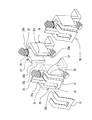
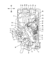
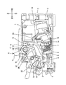
以下、本発明の一実施例を図面に基づいて具体的に説明する。図1は本発明の一実施例の分解斜視図であり、図2は本発明の一実施例を備えるブレーカの側面図である。 Hereinafter, an embodiment of the present invention will be specifically described with reference to the drawings. FIG. 1 is an exploded perspective view of an embodiment of the present invention, and FIG. 2 is a side view of a breaker provided with an embodiment of the present invention.
図2は電源回路に負荷回路を導通させているオン状態における上記ブレーカを示し、図2において前後方向は紙面の表裏方向であり、上下左右の方向は同図に矢印で示す方向である。 FIG. 2 shows the breaker in an on state in which the load circuit is conducted to the power supply circuit. In FIG. 2, the front-rear direction is the front and back direction of the paper, and the upper, lower, left, and right directions are directions indicated by arrows in the figure.
図2に示すブレーカは、ケース1の右端部に電源回路を接続する電源接続端子2を、左端部に負荷回路を接続する負荷接続端子3を備え、又、負荷接続端子3に金属帯材からなる支持片4を介して導通させた固定接点5と、この固定接点5に接離させる可動接点6を備える。
The breaker shown in FIG. 2 includes a
上記固定接点5は上記ケース1に固定され、上記可動接点6は遊動部材7を介して固定接点5の上側で上下に遊動可能に設けられる。
The fixed
この可動接点6を固定接点5に接離させる開閉手段8は、上記遊動部材7を介して可動接点6を上方、即ち、固定接点5から離隔する方向に付勢する付勢手段9と、この付勢手段9に抗して可動端子6を固定接点5に当接させるリンク機構10とを備える。
The opening / closing means 8 for bringing the
このリンク機構10は、作業者が回転操作するハンドル11と、このハンドル11の回転軸心から離れた位置で該ハンドル11に基端部が前後軸心回りに回転自在に支持されているリンク12と、第1支点軸13を中心に回転自在に上記ケース1に支持される開閉部材14と、トリップ部材15とを備える。
The
上記ハンドル11は、上記ケース1に設けたオフ時牽制部1aに受止められるオフ位置と、上記ケース1に設けたオン時牽制部1bに受止められる位置の間で第2支点軸16を中心に前後軸心回りに回転可能に設けられ、戻しバネ17によりオフ位置に付勢されている。
The
上記リンク12の先端部は上記開閉部材14の上面に滑動可能に当接され、作業者がハンドル11をオフ位置からオン位置に移動させると、該リンク12の先端部が上記開閉部材14及び遊動部材7を押し下げて可動接点6を固定接点5に当接させる一方、該リンク12の基端部が上記第2支点軸16と該リンク12の先端部を結ぶ直線の右側から左側に移動し、上記付勢手段9により上記遊動部材7及び開閉部材14を介して上記戻しバネ17に抗してハンドル11をオン位置に付勢することにより上記リンク機構10をオン状態にロックする。
The distal end portion of the
ところで、このブレーカは、負荷回路に過電流が流れると上記トリップ部材15を駆動して、該トリップ部材15が上記リンク12の先端部を上記開閉部材14の上面上に牽制する作用を解除する過電流時トリップ駆動装置18を備える。
By the way, the breaker drives the
図1と図2に示すように、この過電流時トリップ駆動装置18は、上記電源接続端子2と上記遊動部材7を接続する内部回路の部分が挿通される電磁石19と、該電磁石19に駆動されて上記トリップ部材15を駆動する駆動片20と、該駆動片20を上記トリップ部材15から離隔させる戻しバネ21を備える。
As shown in FIGS. 1 and 2, this overcurrent
図1において、前後、左右及び上下は矢印で示している。図1に示すように、上記電磁石19は鉄、鋼などの強磁性体をU字溝形に曲げた吸着部材23を備え、この吸着部材23の溝側壁の端面が駆動片20の被吸着部22を吸着する吸着面23aを構成する。そして、この吸着部材23の内側に形成される溝24に、例えば合成樹脂からなる絶縁チューブ25と、この絶縁チューブ25に挿通された内部回路の一部分が挿入される。
In FIG. 1, front and rear, left and right, and top and bottom are indicated by arrows. As shown in FIG. 1, the
この電磁石19は、この内部回路の一部分を流れる電流により励磁され、上記駆動片20の被吸着部22を吸着する吸着面23aと、この吸着面23aに交差する交差面23bと、これら吸着面23aと交差面23bが交差する稜線23cを備えている。
The
上記駆動片20は1枚の板材又は帯材をワンショットプレス成形したものであり、上記被吸着部22と、該被吸着部22の上縁の一部分、例えば後半部分から延出された駆動部26と、該被吸着部22の上縁部の一部分、例えば前半部分を折り曲げることにより形成されている係合部27とを備える。そして、この駆動片20の上記被吸着部22と係合部27との屈曲部に形成される屈曲凹部28を上記電磁石19の稜線23cに係合させることにより、該駆動片20が上記電磁石19に稜線23cを支点にして前後軸心回りに回転可能に支持される。
The
上記内部回路を流れる電流が所定値以下の場合には、図2に示すように、上記戻しバネ21により、上記駆動片20の電磁石19からの脱落が防止されると共に、被吸着部22が吸着面23aから離れ、その下端部が上記ケース1に設けた駆動片牽制部1cに受止められるオフ位置に弾性支持される。
When the current flowing through the internal circuit is below a predetermined value, the
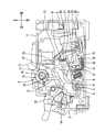
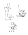
図3は上記内部回路の電流値が所定値を上回り、電磁石19が駆動片20の被吸着部22を吸着し、上記トリップ部材15によるリンク12の牽制が解除された時(以下、トリップ時という。)の上記ブレーカの側面図である。
FIG. 3 shows a case where the current value of the internal circuit exceeds a predetermined value, the
図3に示すように、上記トリップ部材15は上記第1支点軸13に回転自在に支持させた中央部29と、この中央部29から上記開閉部材14の上側に延出されたフック部30と、この中央部29から下方に延出された過電流時受動部31を備えている。
As shown in FIG. 3, the
図1に示すように、オン状態では、上記リンク12の先端部の上記開閉部材14の先端方向への移動はフック部30の先端に形成された鈎先部32により制限され、上記開閉部材14の基端方向への移動は該開閉手段14の上面により制限されている。
As shown in FIG. 1, in the on state, the movement of the distal end portion of the
このオン状態で負荷回路に過電流、あるいは、急激な電流変動が発生すると、上記電磁石19の磁気吸着力が上記戻しバネ21の付勢力に打ち勝ち、図3に示すように、駆動片20の被吸着部22が吸着面23aに吸着され、駆動片20が上記稜線23cを中心に反時計回りの方向に回転し、駆動部26が上記トリップ部材15の過電流時受動部32を左方に移動させ、フック部30の鈎先部32を上記リンク12の先端部の太さよりも大きく開閉部材14の上面から離隔させる。
When an overcurrent or a sudden current fluctuation occurs in the load circuit in this ON state, the magnetic attractive force of the
これにより、フック部30によるリンク12の開閉部材14の先端方向への移動に対する牽制が解除され、リンク12の先端部が開閉部材14の先端方向に滑って開閉部材14、遊動部材7及び可動接点6が上方に移動し、内部回路が開かれる。
As a result, the restraint on the movement of the
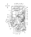
一方、リンク12の先端部が開閉方向14の先端方向に滑ると、ハンドル11は上記付勢手段9による付勢を失い、戻しバネ16により急激にオフ位置に復帰する。そして、図4の側面図に示すように、ハンドル11がオフ位置に復帰すると、上記リンク12の先端部は上記第1支点軸13の方向に引戻される。
On the other hand, when the distal end portion of the
又、上記内部回路が開かれることにより、電磁石19の磁気吸着力が消失し、戻しバネ21により駆動片20がオフ位置に復帰し、この駆動片20のオフ位置への復帰に追随して上記トリップ部材15が自重により上記リンク12の先端部を牽制する位置に復帰し、第1支点軸13側に引戻されたリンク12の先端部は鈎先部32と中央部29間でフック部30と開閉部材14の間に挟まれる。
Further, when the internal circuit is opened, the magnetic attractive force of the
図5はオフ状態における上記ブレーカの側面図である。オフ状態では、上記付勢手段9により付勢されている開閉部材14の先端部の上昇がケース1に設けた左牽制部1dに牽制される。上記付勢手段9により上昇付勢されている遊動部材7の上昇は可動接点16と付勢手段9の間で中間部上記開閉部材14を介して上記左牽制部1eで牽制されると共に、上記付勢手段9よりも左側で上記ケース1に設けた右牽制部1dにより牽制される。そして、この遊動部材7に支持された可動接点6は固定接点5の上側に離隔するオフ位置に保持される。
FIG. 5 is a side view of the breaker in the off state. In the off state, the rise of the tip of the opening / closing
オフ状態からオン状態への切換えは作業者が上記ハンドル11を操作して行うが、この切換えの間は過電流時トリップ駆動装置18の状態は変化しない。
Switching from the off state to the on state is performed by the operator operating the
以上に説明したように、上記駆動片20は、電磁石19に駆動片20を回転可能に支持させるためにピンを用いていないので、電磁石19にこのピンを挿通するピン孔を形成したり、ケース1にこのピンを挿入するピン孔やピンそのものを形成したりする必要がない。その結果、部品点数及び組立工数を削減してブレーカをすこぶる安価に製造できる効果を得ることができる上、電磁石やケースの形状を簡素にしてブレーカを一層安価に製造できる効果を得ることができる。
As described above, since the
又、上記駆動片20に上記ピンが植設されたり挿通されたりする支持部が設けられていないので、材料使用量が少なくなる上、プレスの金型費用及びエネルギ費用を削減でき、以上の諸効果が相乗してすこぶる安価にブレーカを製造できる効果を得ることができる。
Further, since the
更に、この実施例によれば、上記駆動片20に上記ピンが植設されたり挿通されたりする支持部が設けられていないので、駆動片20の慣性重量が軽量になり、応答性が高められる効果を得ることができる。
Furthermore, according to this embodiment, since the
ところで、上記の一実施例では駆動片20を付勢する戻しバネ21が設けられているが、オン状態において上記トリップ部材15の過電流時受動部30を所定のセット圧で上記駆動片20に当接させる別の付勢手段を設け、電磁石19の電磁吸着力が所定値を上回る時にこの付勢手段に抗して駆動片20が上記過電流時受動部30を左方に移動させ、トリップ部材15によるリンク12の牽制が解かれるようにしてもよい。
By the way, in the above embodiment, the
又、上記の一実施例では、駆動片20の駆動部26が被吸着部22と面一の平板上に形成されているが、例えば側面から見てく字形に屈曲させたり、クランク状に屈曲させたりするなど屈曲した形状に形成したり、撚り板形状に形成したりすることが可能である。
In the above-described embodiment, the
更に、上記一実施例においては、上記電磁石19の吸着面23aと交差面との稜線23cにおける挟角は90°にしているが、この挟角は駆動片20がオフ位置からトリップ部材15を駆動して該トリップ部材15によるリンク12の牽制を解除できる位置の間の移動できるように、駆動片20の被吸着部22と係合部27との屈曲凹部28の挟角よりも小さく設定してあればよく、鈍角であってもよく、又、鋭角であってもよい。
Furthermore, in the above-described embodiment, the included angle at the
18 過電流時トリップ駆動装置
19 電磁石
20 駆動片
22 被吸着部
23a 吸着面
23b 交差面
23c 稜線
26 駆動部
27 係合部
28 屈曲凹部
DESCRIPTION OF
Claims (1)
上記電磁石は、上記被吸着部を吸着する吸着面と、この吸着面と交差する交差面と、上記吸着面と交差面とが交わる稜線を備え、上記駆動片は上記電磁石に吸着される被吸着部と、該被吸着部の一端縁の一部分から延出された駆動部と、該被吸着部の一端縁部を部分的に屈曲させた係合部を備え、上記稜線に上記駆動片の被吸着部と係合部との屈曲部に形成される屈曲凹部を係合させることにより上記駆動片を電磁石に回転可能に支持させていることを特徴とするブレーカの過電流時トリップ駆動装置。 In an overcurrent trip driving device for a breaker having an electromagnet and a driving piece driven by the electromagnet to trip the breaker,
The electromagnet includes an attracting surface that attracts the attracted portion, an intersecting surface that intersects the attracting surface, and a ridge line that intersects the attracting surface and the intersecting surface, and the drive piece is attracted to the electromagnet. And a drive part extended from a part of one end edge of the attracted part, and an engaging part obtained by partially bending the one end edge part of the attracted part, An overcurrent trip drive device for a breaker, wherein the drive piece is rotatably supported by an electromagnet by engaging a bent recess formed in a bent portion between an attracting portion and an engaging portion.
Priority Applications (1)
| Application Number | Priority Date | Filing Date | Title |
|---|---|---|---|
| JP2004102954A JP2005293871A (en) | 2004-03-31 | 2004-03-31 | Trip driving device at time of overcurrent of breaker |
Applications Claiming Priority (1)
| Application Number | Priority Date | Filing Date | Title |
|---|---|---|---|
| JP2004102954A JP2005293871A (en) | 2004-03-31 | 2004-03-31 | Trip driving device at time of overcurrent of breaker |
Publications (1)
| Publication Number | Publication Date |
|---|---|
| JP2005293871A true JP2005293871A (en) | 2005-10-20 |
Family
ID=35326595
Family Applications (1)
| Application Number | Title | Priority Date | Filing Date |
|---|---|---|---|
| JP2004102954A Pending JP2005293871A (en) | 2004-03-31 | 2004-03-31 | Trip driving device at time of overcurrent of breaker |
Country Status (1)
| Country | Link |
|---|---|
| JP (1) | JP2005293871A (en) |
Cited By (1)
| Publication number | Priority date | Publication date | Assignee | Title |
|---|---|---|---|---|
| WO2023119895A1 (en) * | 2021-12-20 | 2023-06-29 | パナソニックホールディングス株式会社 | Electromagnetic trip device, circuit breaker, and distribution board |
-
2004
- 2004-03-31 JP JP2004102954A patent/JP2005293871A/en active Pending
Cited By (1)
| Publication number | Priority date | Publication date | Assignee | Title |
|---|---|---|---|---|
| WO2023119895A1 (en) * | 2021-12-20 | 2023-06-29 | パナソニックホールディングス株式会社 | Electromagnetic trip device, circuit breaker, and distribution board |
Similar Documents
| Publication | Publication Date | Title |
|---|---|---|
| US8726755B2 (en) | Shift device | |
| US20110174106A1 (en) | Shift lever device | |
| JP3982143B2 (en) | Lock switch device | |
| JP2005293871A (en) | Trip driving device at time of overcurrent of breaker | |
| JP5981556B2 (en) | Power generation input device and electronic apparatus using the power generation input device | |
| KR100690148B1 (en) | Electromagnetic tripping device for circuit breaker | |
| JPH09199322A (en) | Solenoid | |
| JP4372596B2 (en) | breaker | |
| CN110265267B (en) | Relay with armature capable of stable reset | |
| JP6648651B2 (en) | Electromagnetic relay | |
| JP2005276460A (en) | Electromagnetic switching device | |
| JP5848931B2 (en) | Switch device with reset function | |
| JP4983652B2 (en) | Circuit breaker electromagnetic trip device | |
| JP2008136774A (en) | Solenoid attachment structure for electric variable winning device | |
| JP2007177409A (en) | Electromagnetic solenoid-type drive unit, and furniture or building equipped it | |
| CN1121636A (en) | Electric magnetic contactor | |
| JP2003317596A (en) | Electromagnetic relay | |
| JPS603552Y2 (en) | plunger solenoid | |
| JPH0621160Y2 (en) | Release type electromagnetic trip device for circuit breaker | |
| JP5115236B2 (en) | Electromagnet device | |
| JP2565460Y2 (en) | Fraud prevention structure of winning equipment for pachinko machines | |
| JP3985179B2 (en) | Circuit breaker electromagnetic trip device | |
| JP2009108649A (en) | Door stopper | |
| JP2524757Y2 (en) | Release Release | |
| JP2010287336A (en) | Foot-switch device |
Legal Events
| Date | Code | Title | Description |
|---|---|---|---|
| A621 | Written request for application examination |
Effective date: 20070207 Free format text: JAPANESE INTERMEDIATE CODE: A621 |
|
| A977 | Report on retrieval |
Free format text: JAPANESE INTERMEDIATE CODE: A971007 Effective date: 20090807 |
|
| A131 | Notification of reasons for refusal |
Free format text: JAPANESE INTERMEDIATE CODE: A131 Effective date: 20090819 |
|
| A02 | Decision of refusal |
Free format text: JAPANESE INTERMEDIATE CODE: A02 Effective date: 20100105 |