JP2005293865A - Sample holder and sample tilt holder - Google Patents
Sample holder and sample tilt holder Download PDFInfo
- Publication number
- JP2005293865A JP2005293865A JP2004102815A JP2004102815A JP2005293865A JP 2005293865 A JP2005293865 A JP 2005293865A JP 2004102815 A JP2004102815 A JP 2004102815A JP 2004102815 A JP2004102815 A JP 2004102815A JP 2005293865 A JP2005293865 A JP 2005293865A
- Authority
- JP
- Japan
- Prior art keywords
- sample
- holder
- cartridge
- chip
- tilt
- Prior art date
- Legal status (The legal status is an assumption and is not a legal conclusion. Google has not performed a legal analysis and makes no representation as to the accuracy of the status listed.)
- Granted
Links
Images
Landscapes
- Sampling And Sample Adjustment (AREA)
Abstract
【課題】 試料を2軸傾斜ホルダへ容易に配置することができる試料ホルダを提供する。
【解決手段】 21は棒状の導入部であり、導入部21は透過電子顕微鏡のゴニオメータに装着できるように形成されている。22はチップオンカートリッジであり、チップオンカートリッジ22は取付部23とシャトル(試料保持部)24とで構成されている。本発明のチップオンカートリッジ22は、従来のチップオンカートリッジが2つに分割されて構成されている。取付部23の一端は導入部21の先端に着脱可能に取り付けられるように形成されている。シャトル24は取付部23の他端に着脱可能に取り付けられるように形成されている。このため、シャトル24を取付部23に取り付けると共に、取付部23を導入部21の先端に取り付けると、図4(b)に示す試料ホルダ20となる。
【選択図】 図4
PROBLEM TO BE SOLVED: To provide a sample holder capable of easily arranging a sample on a biaxial tilt holder.
SOLUTION: 21 is a rod-shaped introduction part, and the introduction part 21 is formed so that it can be attached to a goniometer of a transmission electron microscope. Reference numeral 22 denotes a chip-on cartridge. The chip-on cartridge 22 includes an attachment portion 23 and a shuttle (sample holding portion) 24. The chip-on cartridge 22 of the present invention is configured by dividing a conventional chip-on cartridge into two. One end of the attachment portion 23 is formed to be detachably attached to the distal end of the introduction portion 21. The shuttle 24 is formed to be detachably attached to the other end of the attachment portion 23. For this reason, when the shuttle 24 is attached to the attachment portion 23 and the attachment portion 23 is attached to the tip of the introduction portion 21, the sample holder 20 shown in FIG.
[Selection] Figure 4
Description
本発明は、透過電子顕微鏡や集束イオンビーム加工装置などに装着される試料ホルダ、および透過電子顕微鏡などの試料観察装置に装着される試料傾斜ホルダに関する。 The present invention relates to a sample holder mounted on a transmission electron microscope, a focused ion beam processing apparatus, and the like, and a sample tilt holder mounted on a sample observation apparatus such as a transmission electron microscope.
透過電子顕微鏡(TEM)においては、電子銃からの電子線が試料に照射され、試料を透過した電子線によって形成された透過電子顕微鏡像(TEM像)や回折像は、電子線光軸上に配置された蛍光板などによってTEM観察される。
このような透過電子顕微鏡で観察される試料は、照射電子線が透過するように薄く作製される。その試料作製装置として集束イオンビーム(FIB)加工装置が用いられており、図1は、集束イオンビーム加工装置を用いた試料作製手順を示した図である。
この場合、まず図1(a)に示すように、試料素材(たとえば半導体基板)からL字状に切り出された試料ブロック1は、C字状に形成された半切りの単孔メッシュ2に貼り付けられる。試料ブロック1は2mm程度と小さいため、試料作製者はピンセットで試料ブロック1を摘んで単孔メッシュ2に貼り付ける。こうして、試料ブロック1と単孔メッシュ2によって試料3が形成される。
次に図1(b)に示すように、試料3はチップオンカートリッジ4にセットされる。この際、試料3は板バネ5によって押しつけられてチップオンカートリッジ4に固定される。単孔メッシュ2は3mm程度と小さく、このため試料3は小さいので、試料作製者はピンセットで試料3を摘んでチップオンカートリッジ4にセットする。
次に図1(c)に示すように、チップオンカートリッジ4はFIB加工装置用試料ホルダ6にセットされる。チップオンカートリッジ4の長さは5cm程あるので、試料作製者はチップオンカートリッジ4を手で直接摘んでFIB加工装置用試料ホルダ6にセットする。FIB加工装置用試料ホルダ6はチップオンカートリッジ4を4個セットできるように構成されている。
次に、FIB加工装置用試料ホルダ6はFIB加工装置(図示せず)に装着される。そして、集束イオンビームが試料3の試料ブロック1上で走査され、試料ブロック1に対してFIB加工(薄膜加工)が行われる。この薄膜加工により、図1(d)に示すように、薄膜部分1aが試料ブロック1に形成される。
すべての試料ブロック(この場合は4個の試料ブロック)に対するFIB加工が終了すると、試料作製者は、FIB加工装置からFIB加工装置用試料ホルダ6を取り出す。そして試料作製者は、FIB加工装置用試料ホルダ6から1個のチップオンカートリッジ4を手で摘んで取り外し、そのチップオンカートリッジ4を図2(a)に示すTEM用試料ホルダ導入部7の先端にセットする。TEM用試料ホルダ導入部7は棒状に形成されており、チップオンカートリッジ4は導入部7の先端に着脱可能に取り付けられる。
次に試料作製者は、図2(b)に示すように、チップオンカートリッジ4を保持したTEM用試料ホルダ導入部7を透過電子顕微鏡のゴニオメータ8に装着する。このゴニオメータ8は、試料3をX,Y,Z軸方向に移動、およびY軸回りに回動(傾斜)させるための移動機構である。こうして、チップオンカートリッジ4上の試料3が対物レンズポールピース9a,9b間に配置されると、電子線が試料3の薄膜部分1a(図1(d)参照)に照射され、試料3のTEM観察が行われる。
このTEM観察が終了すると、試料作製者は、前記ゴニオメータ8からTEM用試料ホルダ導入部7を取り出し、その導入部7からチップオンカートリッジ4を手で摘んで取り外す。そして試料作製者は、上述したTEM観察の際に「試料3の薄膜部分1aをもう少し薄くした方が良い」と判断した場合には、その試料3を保持したチップオンカートリッジ4を前記FIB加工装置用試料ホルダ6に戻す(図1(c)参照)。
このようなTEM観察は残り3個の試料についても順次行われ、「薄膜部分1aをもう少し薄くした方が良いと判断された試料3」を保持したチップオンカートリッジ4は、前記FIB加工装置用試料ホルダ6に戻される。そして、そのFIB加工装置用試料ホルダ6は前記FIB装置に再び装着され、各試料3の薄膜部分1aが更にFIB加工(薄膜加工)される。その後、上述したTEM観察が再び行われる。以後、試料3の薄膜部分1aの厚さがTEM観察に適当な厚さに達するまで、上述したFIB加工とTEM観察が繰り返し行われる。
以上説明した従来技術においては、FIB加工装置と透過電子顕微鏡に共通のチップオンカートリッジ4が採用されている。このチップオンカートリッジ4は手で直接つかみやすい大きさなので、試料作製者は、チップオンカートリッジ4を容易にFIB加工装置用試料ホルダ6とTEM用試料ホルダ導入部7に対して着脱できる。このため、試料作製者は、FIB加工とTEM観察の繰り返しを容易に行うことができる。
なお、チップオンカートリッジについて記載された特許文献として、たとえば特許第2934308号公報(特許文献1)が知られている。
ところで、試料の種類によっては、試料をさらに詳しく観察するためにTEM用2軸傾斜ホルダが必要となる。すなわち、単結晶基板の試料などを透過電子顕微鏡で正確に解析するには、図3に示すような2軸傾斜ホルダ10が必要となる。
図3に示す2軸傾斜ホルダ10は、前記ゴニオメータ8に装着可能な棒状導入部11と、導入部11の先端に形成された傾斜部12とで構成されている。そして傾斜部12は、導入部11先端に固定されたフレーム13と、フレーム13に支持された傾斜軸14と、傾斜軸14上に固定された傾斜台15とを備えている。傾斜台15には電子線通過孔16が開けられており、その電子線通過孔16の周縁に試料載置部17が形成されている。この試料載置部17には、前記チップオンカートリッジ4にセットされてFIB加工された試料3がセットされる。
さて、前記傾斜軸14は、導入部11の中心軸gに直交する軸h上に位置している。そして傾斜軸14は、導入部11内部に組み込まれたモータ(図示せず)の駆動によって、軸h回りに正逆両方向に回転される。それに伴い、傾斜台15は軸h回りに回動される。このように図3に示す2軸傾斜ホルダ10は、傾斜台15上に載置される試料3を軸h回りに傾斜(回動)できるように構成されている。また、2軸傾斜ホルダ10が前記ゴニオメータ8に装着されてゴニオメータ8によってY軸回りに回動されると、それに伴って、試料3はY軸回りに傾斜(回動)される。
以上説明した2軸傾斜ホルダ10を用いることにより、試料3を2つの軸(h,Y)回りに傾斜させることができ、単結晶基板の試料などを正確に解析することができる。
In a transmission electron microscope (TEM), a sample is irradiated with an electron beam from an electron gun, and a transmission electron microscope image (TEM image) or diffraction image formed by the electron beam transmitted through the sample is placed on the electron beam optical axis. TEM observation is performed using a fluorescent screen or the like.
The sample observed with such a transmission electron microscope is made thin so that an irradiation electron beam may permeate | transmit. A focused ion beam (FIB) processing apparatus is used as the sample preparation apparatus, and FIG. 1 is a diagram showing a sample preparation procedure using the focused ion beam processing apparatus.
In this case, as shown in FIG. 1A, a
Next, as shown in FIG. 1B, the
Next, as shown in FIG. 1C, the chip-on cartridge 4 is set in the
Next, the FIB processing
When the FIB processing for all sample blocks (in this case, four sample blocks) is completed, the sample creator takes out the FIB processing
Next, as shown in FIG. 2B, the sample creator attaches the TEM sample holder introducing portion 7 holding the chip-on cartridge 4 to the goniometer 8 of the transmission electron microscope. The goniometer 8 is a moving mechanism for moving the
When this TEM observation is completed, the sample maker takes out the TEM sample holder introducing portion 7 from the goniometer 8, and picks and removes the chip-on cartridge 4 from the introducing portion 7 by hand. When the sample creator determines that the thin film portion 1a of the
Such TEM observation is sequentially performed on the remaining three samples, and the chip-on cartridge 4 holding “
In the conventional technology described above, a chip-on cartridge 4 common to the FIB processing apparatus and the transmission electron microscope is employed. Since the chip-on cartridge 4 is of a size that can be easily grasped by hand, the sample creator can easily attach and detach the chip-on cartridge 4 to the FIB processing
As a patent document describing a chip-on cartridge, for example, Japanese Patent No. 2934308 (Patent Document 1) is known.
By the way, depending on the type of sample, in order to observe the sample in more detail, a biaxial tilt holder for TEM is required. That is, in order to accurately analyze a sample of a single crystal substrate with a transmission electron microscope, a
A
The
By using the
しかしながら、図3に示した2軸傾斜ホルダ10を用いる場合には、前記チップオンカートリッジ4にセットされてFIB加工された試料3を、チップオンカートリッジ4から取り外して2軸傾斜ホルダ10に移さなければならい。その際、試料3は上述したように小さいため、試料作製者はピンセットなどで小さな試料3を摘んで2軸傾斜ホルダ10にセットしなければならい。このような作業には手先の器用さと集中力を要し、この作業は試料作製者にとって非常に煩わしいものである。
本発明はこのような点に鑑みて成されたもので、その目的の1つは、試料を2軸傾斜ホルダへ容易に配置することができる試料ホルダを提供することにある。
However, when the
The present invention has been made in view of the above points, and one of its purposes is to provide a sample holder capable of easily arranging a sample on a biaxial inclined holder.
上記目的を達成する本発明の試料ホルダは、試料観察装置またはイオンビーム照射装置に装着される試料ホルダであって、棒状の導入部と、前記導入部の先端に着脱可能に取り付けられる取付部と、試料を保持するための試料保持部であって、前記取付部に着脱可能に取り付けられる試料保持部とを備えている。 A sample holder of the present invention that achieves the above object is a sample holder that is mounted on a sample observation device or an ion beam irradiation device, and includes a rod-like introduction portion, and an attachment portion that is detachably attached to the tip of the introduction portion. A sample holding unit for holding the sample, the sample holding unit being detachably attached to the attachment portion.
したがって本発明によれば、試料を2軸傾斜ホルダへ容易に配置することができる試料ホルダを提供できる。 Therefore, according to this invention, the sample holder which can arrange | position a sample to a biaxial inclination holder easily can be provided.
以下、図面を用いて本発明の実施の形態について説明する。 Hereinafter, embodiments of the present invention will be described with reference to the drawings.
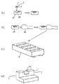
図4は本発明の試料ホルダの一例を示した図であり、透過電子顕微鏡の前記ゴニオメータ8(図2(b)参照)に装着可能な試料ホルダ20を示した図である。なお、図4(a)は本発明の試料ホルダ20をばらした状態を示した図であり、図4(b)は組み立てられた状態の試料ホルダ20を示した図である。
FIG. 4 is a view showing an example of the sample holder of the present invention, and is a view showing the
図4において、21は棒状の導入部である。導入部21は前記ゴニオメータ8に装着できるように形成されており、その形状は前記TEM用試料ホルダ導入部7(図2参照)と同じである。
In FIG. 4, 21 is a rod-shaped introduction part. The
22はチップオンカートリッジであり、チップオンカートリッジ22は取付部23とシャトル(試料保持部)24とで構成されている。このように本発明のチップオンカートリッジ22は、従来のチップオンカートリッジ4(図1参照)が2つに分割されて構成されている。
さて、前記取付部23の一端は、前記導入部21の先端に着脱可能に取り付けられるように形成されている。また、前記シャトル24は、取付部23の他端に着脱可能に取り付けられるように形成されている。このため、シャトル24を取付部23に取り付けると共に、取付部23を導入部21の先端に取り付けると、図4(b)に示す試料ホルダ20が組み上がる。なお、前記シャトル24には、試料を固定するための板バネ25が取り付けられている。
Now, one end of the
以上、図4の試料ホルダ20の構成を説明した。以下、図5を用い、試料ホルダ20を用いた試料のFIB加工について説明する。
まず図5(a)に示すように、前記試料3はシャトル24にセットされる。この際、試料3は板バネ25によって押しつけられてシャトル24に固定される。前記単孔メッシュ2は3mm程度と小さく、このため試料3は小さいので、試料作製者はピンセットで試料3を摘んでシャトル24にセットする。
次に図5(b)に示すように、試料3を保持したシャトル24は取付部26にセットされる。シャトル24の長さは2cm程あり、また取付部23の長さは3cm程あるので、試料作製者はそれらを手で直接摘んでシャトル24を取付部23にセットする。このようにシャトル24と取付部23とが組み合わされて、チップオンカートリッジ22が形成される。
次に図5(c)に示すように、チップオンカートリッジ22は前記FIB加工装置用試料ホルダ6にセットされる。チップオンカートリッジ22の長さは5cm程あるので、試料作製者はチップオンカートリッジ22を手で直接摘んでFIB加工装置用試料ホルダ6にセットする。試料作製者は、用意した4個のチップオンカートリッジ22をFIB加工装置用試料ホルダ6にセットする。
次に、FIB加工装置用試料ホルダ6はFIB加工装置(図示せず)に装着される。そして、集束イオンビームが試料3の試料ブロック1上で走査され、試料ブロック1に対してFIB加工(薄膜加工)が行われる。この薄膜加工により、図5(d)に示すように、薄膜部分1aが試料ブロック1に形成される。
4個の試料に対するFIB加工が終了すると、試料作製者は、FIB加工装置からFIB加工装置用試料ホルダ6を取り出す。そして試料作製者は、FIB加工装置用試料ホルダ6から1個のチップオンカートリッジ22を手で摘んで取り外し、そのチップオンカートリッジ22を図4に示した導入部21の先端にセットする(図4(b)参照)。
次に試料作製者は、チップオンカートリッジ22を保持した導入部21、すなわち試料ホルダ20を透過電子顕微鏡のゴニオメータ8に装着する(図2(b)参照)。こうして、チップオンカートリッジ22上の試料3が対物レンズポールピース間に配置されると、電子線が試料3の薄膜部分1aに照射され、試料3のTEM観察が行われる。
このTEM観察が終了すると、試料作製者は、前記ゴニオメータ8から試料ホルダ20を取り出し、導入部21からチップオンカートリッジ22を手で摘んで取り外す。そして試料作製者は、TEM観察の際に「試料3の薄膜部分1aをもう少し薄くした方が良い」と判断した場合には、その試料3を保持したチップオンカートリッジ22を前記FIB加工装置用試料ホルダ6に戻す(図5(c)参照)。
このようなTEM観察は残り3個の試料についても順次行われ、「薄膜部分1aをもう少し薄くした方が良いと判断された試料3」を保持したチップオンカートリッジ22は、前記FIB加工装置用試料ホルダ6に戻される。そして、そのFIB加工装置用試料ホルダ6は前記FIB装置に再び装着され、各試料3の薄膜部分1aが更にFIB加工(薄膜加工)される。その後、上述したTEM観察が再び行われる。以後、試料3の薄膜部分1aの厚さがTEM観察に適当な厚さに達するまで、上述したFIB加工とTEM観察が繰り返し行われる。
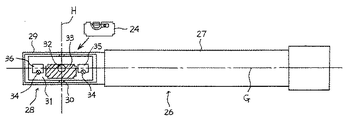
さて、今観察されている試料3がたとえば単結晶基板の場合、試料作製者は試料3をさらに詳しくTEM解析するために、図6に示す本発明の2軸傾斜ホルダ(試料傾斜ホルダ)26を利用する。
図6に示す2軸傾斜ホルダ26は、前記ゴニオメータ8に装着可能な棒状導入部27と、導入部27の先端に形成された傾斜部28とで構成されている。そして傾斜部28は、導入部27先端に固定されたフレーム29と、フレーム29に支持された傾斜軸30と、傾斜軸30上に固定された傾斜台31とを備えている。傾斜台31には電子線通過孔32が開けられている。そして、電子線通過孔32の周縁には、前記シャトル24をセットするための試料載置部33が形成されている。
そこで試料作製者は、前記チップオンカートリッジ22(図5(b)参照)からシャトル24を取り外し、試料3を保持したシャトル24を試料載置部33にセットする。上述したようにシャトル24の長さは2cm程あるので、試料作製者はシャトル24を手で直接摘んで試料載置部33にセットすることができる。このように本発明によれば、試料を2軸傾斜ホルダへ容易にセットすることができる。なお、この試料セットの際、ピンセットでシャトル24を摘んで試料載置部33にセットするようにしても良い。その場合にも試料作製者は、従来のように小さな試料3をピンセットなどで摘んで2軸傾斜ホルダにセットするのに比べ、容易に試料を2軸傾斜ホルダにセットすることができる。
こうしてシャトル24が試料載置部33にセットされると、試料作製者は、傾斜台31にネジ(34)止めされた板バネ(保持手段)35,36を回転させて、板バネ35,36をシャトル24端部上に位置させる。この結果、シャトル24は板バネ35,36によって押しつけられて傾斜台31に固定される。
さて、前記傾斜軸30は、導入部27の中心軸Gに直交する軸H上に位置している。そして傾斜軸30は、導入部27内部に組み込まれたモータ(図示せず)の駆動によって、軸H回りに正逆両方向に回転される。それに伴い、傾斜台31は軸H回りに回動される。
このように図6に示す2軸傾斜ホルダ26は、傾斜台31上に載置される試料3を軸H回りに傾斜(回動)できるように構成されている。また、2軸傾斜ホルダ26が前記ゴニオメータ8に装着されてゴニオメータ8によってY軸回りに回動されると、それに伴って、試料3はY軸回りに傾斜(回動)される。このため、このような2軸傾斜ホルダ26を用いることにより、試料3を2つの軸(H,Y)回りに傾斜させることができ、単結晶基板の試料などを正確に解析することができる。
以上、図4〜図6を用いて本発明の一例を説明したが、本発明においては、チップオンカートリッジ22全体を前記傾斜台31にセットするのではなく、シャトル24のみを傾斜台31にセットするようにしている。このため、傾斜台31にかかる負荷を抑えることができ、傾斜台31をモータ駆動によって精度良く傾斜させることができる。また、シャトル24のみを傾斜台31にセットするようにしているので、傾斜台31を小型化することができ、ひいては2軸傾斜ホルダ全体を小型化することができる。
なお、本発明は上記例に限定されるものではない。たとえば、図4に示した試料ホルダ20を装着できるFIB加工装置を用意すれば、その試料ホルダ20をFIB加工装置と透過電子顕微鏡間で差し替えるだけで、FIB加工とTEM観察の繰り返しをより容易に行うことができる。また、集束イオンビーム装置の代わりに、一度に試料上の広範囲にイオンビームを照射するタイプのイオンビーム照射装置を用いるようにしても良い。
また、上述した本発明の試料ホルダや2軸傾斜ホルダを透過電子顕微鏡以外の試料観察装置、たとえば走査電子顕微鏡や電子プローブマイクロアナライザなどに適用するようにしても良い。
The configuration of the
First, as shown in FIG. 5A, the
Next, as shown in FIG. 5B, the
Next, as shown in FIG. 5C, the chip-on
Next, the FIB processing
When the FIB processing for the four samples is completed, the sample creator takes out the FIB processing
Next, the sample creator attaches the
When this TEM observation is completed, the sample maker takes out the
Such TEM observation is sequentially performed on the remaining three samples, and the chip-on
Now, when the
A
Therefore, the sample creator removes the
When the
The
As described above, the
As described above, an example of the present invention has been described with reference to FIGS. 4 to 6. In the present invention, the entire chip-on
The present invention is not limited to the above example. For example, if an FIB processing apparatus capable of mounting the
Further, the above-described sample holder and biaxial tilt holder of the present invention may be applied to a sample observation apparatus other than a transmission electron microscope, such as a scanning electron microscope or an electron probe microanalyzer.
1…試料ブロック、2…単孔メッシュ、3…試料、4…チップオンカートリッジ、5…板バネ、6…FIB加工装置用試料ホルダ、7…TEM用試料ホルダ導入部、8…ゴニオメータ、9a,9b…対物レンズポールピース、10…2軸傾斜ホルダ、11…導入部、12…傾斜部、13…フレーム、14…傾斜軸、15…傾斜台、16…電子線通過孔、17…試料載置部、20…試料ホルダ、21…導入部、22…チップオンカートリッジ、23…取付部、24…シャトル、25…板バネ、26…2軸傾斜ホルダ、27…導入部、28…傾斜部、29…フレーム、30…傾斜軸、31…傾斜台、32…電子線通過孔、33…試料載置台、34…ネジ、35,36…板バネ
DESCRIPTION OF
Claims (2)
(a)棒状の導入部
(b)前記導入部の先端に着脱可能に取り付けられる取付部
(c)試料を保持するための試料保持部であって、前記取付部に着脱可能に取り付けられる試料保持部。 A sample holder mounted on a sample observation device or an ion beam irradiation device, comprising the following components (a) to (c): a sample holder (a) a rod-shaped introduction portion (b) A mounting part (c) that is detachably attached to the tip of the introduction part. A sample holding part for holding a sample, the sample holding part being detachably attached to the mounting part.
前記傾斜台は、上記請求項1における試料保持部を保持するための保持手段を備えていることを特徴とする試料傾斜ホルダ。
A sample tilt holder comprising a rod-shaped introduction portion and a tilt base that can be tilted about an axis substantially orthogonal to the central axis of the introduction portion,
2. The sample tilt holder according to claim 1, wherein the tilt table includes a holding means for holding the sample holding portion according to claim 1.
Priority Applications (1)
| Application Number | Priority Date | Filing Date | Title |
|---|---|---|---|
| JP2004102815A JP4351103B2 (en) | 2004-03-31 | 2004-03-31 | Sample holder and sample tilt holder |
Applications Claiming Priority (1)
| Application Number | Priority Date | Filing Date | Title |
|---|---|---|---|
| JP2004102815A JP4351103B2 (en) | 2004-03-31 | 2004-03-31 | Sample holder and sample tilt holder |
Publications (2)
| Publication Number | Publication Date |
|---|---|
| JP2005293865A true JP2005293865A (en) | 2005-10-20 |
| JP4351103B2 JP4351103B2 (en) | 2009-10-28 |
Family
ID=35326589
Family Applications (1)
| Application Number | Title | Priority Date | Filing Date |
|---|---|---|---|
| JP2004102815A Expired - Fee Related JP4351103B2 (en) | 2004-03-31 | 2004-03-31 | Sample holder and sample tilt holder |
Country Status (1)
| Country | Link |
|---|---|
| JP (1) | JP4351103B2 (en) |
Cited By (5)
| Publication number | Priority date | Publication date | Assignee | Title |
|---|---|---|---|---|
| JP2010055988A (en) * | 2008-08-29 | 2010-03-11 | Jeol Ltd | Thin film sample observation system, cooling sample holder, and thin film sample observation method |
| CN102353580A (en) * | 2011-06-22 | 2012-02-15 | 北京工业大学 | Uniaxial tension sample holder capable of testing in-situ stress and electrical property for transmission electron microscope |
| EP2824448A1 (en) * | 2013-07-08 | 2015-01-14 | Bruker Nano GmbH | Sample holder for electron backscatter diffraction |
| EP3153852A4 (en) * | 2014-06-04 | 2018-01-03 | Hamamatsu Photonics K.K. | Inspection device and method for disposing magneto-optical crystal |
| JP2018077966A (en) * | 2016-11-08 | 2018-05-17 | 日本電子株式会社 | Cartridge holding device |
Families Citing this family (1)
| Publication number | Priority date | Publication date | Assignee | Title |
|---|---|---|---|---|
| CN104916516B (en) * | 2015-05-26 | 2017-03-22 | 兰州大学 | Transmission electron microscope sample rod capable of realizing electric and magnetic field loading |
-
2004
- 2004-03-31 JP JP2004102815A patent/JP4351103B2/en not_active Expired - Fee Related
Cited By (7)
| Publication number | Priority date | Publication date | Assignee | Title |
|---|---|---|---|---|
| JP2010055988A (en) * | 2008-08-29 | 2010-03-11 | Jeol Ltd | Thin film sample observation system, cooling sample holder, and thin film sample observation method |
| CN102353580A (en) * | 2011-06-22 | 2012-02-15 | 北京工业大学 | Uniaxial tension sample holder capable of testing in-situ stress and electrical property for transmission electron microscope |
| EP2824448A1 (en) * | 2013-07-08 | 2015-01-14 | Bruker Nano GmbH | Sample holder for electron backscatter diffraction |
| EP3153852A4 (en) * | 2014-06-04 | 2018-01-03 | Hamamatsu Photonics K.K. | Inspection device and method for disposing magneto-optical crystal |
| US10139370B2 (en) | 2014-06-04 | 2018-11-27 | Hamamatsu Photonics K.K. | Inspection device and method for disposing magneto-optical crystal |
| TWI645208B (en) * | 2014-06-04 | 2018-12-21 | 日商濱松赫德尼古斯股份有限公司 | Inspection device and configuration method of magnetic optical crystal |
| JP2018077966A (en) * | 2016-11-08 | 2018-05-17 | 日本電子株式会社 | Cartridge holding device |
Also Published As
| Publication number | Publication date |
|---|---|
| JP4351103B2 (en) | 2009-10-28 |
Similar Documents
| Publication | Publication Date | Title |
|---|---|---|
| US6927400B2 (en) | Sample manipulation system | |
| JP2002333387A (en) | Beam member, sample processing apparatus using beam member, and sample extracting method | |
| JP3407101B2 (en) | A microscope that can be observed simultaneously with an electron microscope and a scanning tunneling microscope under ultra-high vacuum | |
| CN106248447A (en) | The method of the sample of preparation micro structure diagnosis and the sample of micro structure diagnosis | |
| JP4351103B2 (en) | Sample holder and sample tilt holder | |
| US7067823B2 (en) | Micro-sample pick-up apparatus and micro-sample pick-up method | |
| JP2009216534A (en) | Thin-film sample preparation method | |
| JP2007188905A (en) | Sample holder for charged particle beam equipment | |
| US8008635B2 (en) | Method for sample preparation | |
| JP2934308B2 (en) | Sample holder for transmission electron microscope | |
| JP4898355B2 (en) | Sample holder | |
| JP5189471B2 (en) | Microscope observation equipment | |
| JP4055066B2 (en) | Sample holder for electron microscope | |
| JP2013080605A (en) | Sample holder tip, sample holder, and manufacturing method of sample holder tip | |
| JP3106846U (en) | Sample holder for charged particle beam equipment | |
| JP2013134978A (en) | Sample support for transmission electron microscope, transmission electron microscope and three-dimensional structure observation method of sample | |
| DE112015005875B4 (en) | MASK POSITION ADJUSTMENT PROCEDURE FOR ION MILLING, ELECTRON MICROSCOPE FOR ADJUSTING THE MASK POSITION, MASK ADJUSTMENT MOUNTED ON A SAMPLE STAGE AND SAMPLE MASK COMPONENTS OF AN ION MILLING DEVICE | |
| JP4784888B2 (en) | Method for preparing sample for atom probe analysis by FIB and apparatus for implementing the same | |
| JP2012155870A (en) | Specimen holder and specimen holder driving device | |
| JPH04324240A (en) | Electron microscope sample holeder and retaining method for sample | |
| JP2004199969A (en) | Sample holder for charged particle beam equipment | |
| JP2002150984A (en) | Sample holder | |
| JP2004309499A (en) | Sample preparation apparatus and sample preparation method | |
| KR0150675B1 (en) | Method of making samples with tem | |
| JP2022107299A (en) | Sample holder and charged particle beam device |
Legal Events
| Date | Code | Title | Description |
|---|---|---|---|
| A621 | Written request for application examination |
Free format text: JAPANESE INTERMEDIATE CODE: A621 Effective date: 20061130 |
|
| A977 | Report on retrieval |
Free format text: JAPANESE INTERMEDIATE CODE: A971007 Effective date: 20081120 |
|
| A131 | Notification of reasons for refusal |
Free format text: JAPANESE INTERMEDIATE CODE: A131 Effective date: 20081216 |
|
| A521 | Request for written amendment filed |
Free format text: JAPANESE INTERMEDIATE CODE: A523 Effective date: 20090212 |
|
| A131 | Notification of reasons for refusal |
Free format text: JAPANESE INTERMEDIATE CODE: A131 Effective date: 20090519 |
|
| A521 | Request for written amendment filed |
Free format text: JAPANESE INTERMEDIATE CODE: A523 Effective date: 20090529 |
|
| TRDD | Decision of grant or rejection written | ||
| A01 | Written decision to grant a patent or to grant a registration (utility model) |
Free format text: JAPANESE INTERMEDIATE CODE: A01 Effective date: 20090714 |
|
| A01 | Written decision to grant a patent or to grant a registration (utility model) |
Free format text: JAPANESE INTERMEDIATE CODE: A01 |
|
| A61 | First payment of annual fees (during grant procedure) |
Free format text: JAPANESE INTERMEDIATE CODE: A61 Effective date: 20090723 |
|
| FPAY | Renewal fee payment (event date is renewal date of database) |
Free format text: PAYMENT UNTIL: 20120731 Year of fee payment: 3 |
|
| R150 | Certificate of patent or registration of utility model |
Ref document number: 4351103 Country of ref document: JP Free format text: JAPANESE INTERMEDIATE CODE: R150 Free format text: JAPANESE INTERMEDIATE CODE: R150 |
|
| FPAY | Renewal fee payment (event date is renewal date of database) |
Free format text: PAYMENT UNTIL: 20120731 Year of fee payment: 3 |
|
| FPAY | Renewal fee payment (event date is renewal date of database) |
Free format text: PAYMENT UNTIL: 20130731 Year of fee payment: 4 |
|
| FPAY | Renewal fee payment (event date is renewal date of database) |
Free format text: PAYMENT UNTIL: 20130731 Year of fee payment: 4 |
|
| LAPS | Cancellation because of no payment of annual fees |