JP2005293768A - Optical recording medium - Google Patents
Optical recording medium Download PDFInfo
- Publication number
- JP2005293768A JP2005293768A JP2004109960A JP2004109960A JP2005293768A JP 2005293768 A JP2005293768 A JP 2005293768A JP 2004109960 A JP2004109960 A JP 2004109960A JP 2004109960 A JP2004109960 A JP 2004109960A JP 2005293768 A JP2005293768 A JP 2005293768A
- Authority
- JP
- Japan
- Prior art keywords
- layer
- recording
- magnetic
- magnetic field
- temperature
- Prior art date
- Legal status (The legal status is an assumption and is not a legal conclusion. Google has not performed a legal analysis and makes no representation as to the accuracy of the status listed.)
- Pending
Links
Images


Abstract
【課題】 本発明は、外部記録磁界Hwを印加しなくても、スポット径に比して微細な高密度記録パターンを安定に光変調方式でダイレクトオーバーライト記録できる光学的記録媒体を提供することを目的とする。
【解決手段】 本発明は、メモリ層、書き込み層、遮断層、及び初期化層を有し、DTE方式の情報記録方法に用いられる光学的記録媒体において、初期化層上に、書き込み層に対して漏洩磁界を発生させる垂直磁化膜から成る記録磁界層と、該記録磁界層の磁化を交換結合により膜面内方向に配向させる磁性膜から成る面内磁化誘導層と、面内磁化誘導層と記録磁界層との間に、室温において交換結合し、かつ、面内磁化誘導層および記録磁界層よりもキュリー温度の低い磁性層から成る第二遮断層とが積層されていることを特徴とする光学的記録媒体。
【選択図】 図1PROBLEM TO BE SOLVED: To provide an optical recording medium capable of stably directly overwriting a high-density recording pattern finer than the spot diameter by a light modulation method without applying an external recording magnetic field Hw. With the goal.
An optical recording medium having a memory layer, a writing layer, a blocking layer, and an initialization layer, and used for a DTE information recording method, on the initialization layer and with respect to the writing layer. A recording magnetic field layer made of a perpendicular magnetization film that generates a leakage magnetic field, an in-plane magnetization induction layer made of a magnetic film that orients the magnetization of the recording magnetic field layer in the in-plane direction by exchange coupling, and an in-plane magnetization induction layer, A second blocking layer comprising a magnetic layer having exchange coupling at room temperature and having a Curie temperature lower than that of the recording magnetic layer is laminated between the recording magnetic layer and room temperature. Optical recording medium.
[Selection] Figure 1
Description
本発明は、光ビームの強度、パルス幅を変調する、所謂光変調により情報のオーバーライト記録を行う光学的記録媒体に関するものであり、特に光ビームのスポットサイズ以下の記録マークを含む高密度記録を行うための光学的記録媒体に関するものである。 The present invention relates to an optical recording medium for performing information overwrite recording by so-called light modulation, which modulates the intensity and pulse width of a light beam, and in particular, high-density recording including a recording mark having a size equal to or smaller than the spot size of the light beam. The present invention relates to an optical recording medium for performing the above.
書き換え可能な記録媒体として、各種の磁性記録媒体が実用化されている。特に、半導体レーザの熱エネルギーを用いて磁性薄膜に磁区を書き込んで情報を記録し、磁気光学効果を用いてこの情報を読み出す光磁気記録媒体は、高密度記録が可能な大容量可換媒体として期待されている。近年、動画像のデジタル化の動きとあいまって、これらの磁性記録媒体の記録密度を高めて、さらに大容量の記録媒体とする要求が高まっている。 Various magnetic recording media have been put to practical use as rewritable recording media. In particular, a magneto-optical recording medium that records information by writing magnetic domains in a magnetic thin film using the thermal energy of a semiconductor laser and reads this information using the magneto-optic effect is a large-capacity replaceable medium capable of high-density recording. Expected. In recent years, coupled with the trend toward digitization of moving images, there is an increasing demand for recording media of these magnetic recording media to have higher recording density and higher capacity.
一般に、光記録媒体の線記録密度は、再生光学系のレーザ波長および対物レンズの開口数NAに大きく依存する。すなわち、再生光学系のレーザ波長λと対物レンズの開口数NAが決まると、ビームウェストの径が決まるため、信号再生可能な記録ピットの空間周波数は2NA/λ程度が限界となってしまう。したがって、従来の光ディスクで高密度化を実現するためには、再生光学系のレーザ波長を短くするか、対物レンズの開口数を大きくする必要がある。 In general, the linear recording density of an optical recording medium greatly depends on the laser wavelength of the reproducing optical system and the numerical aperture NA of the objective lens. That is, when the laser wavelength λ of the reproducing optical system and the numerical aperture NA of the objective lens are determined, the diameter of the beam waist is determined, so that the spatial frequency of the recording pits capable of signal reproduction is limited to about 2 NA / λ. Therefore, in order to realize high density with the conventional optical disc, it is necessary to shorten the laser wavelength of the reproducing optical system or increase the numerical aperture of the objective lens.
レーザ波長は、波長が635nm〜685nm付近の従来の赤色半導体レーザに対して、波長が約405nm、435nm付近の短波長の青色半導体レーザが開発され実用化が進んでいる。しかしながら、レーザ波長をこれ以上短くすると紫外線の領域に入り、紫外線を透過する材料が限られる等の問題が発生し、記録用再生用として、これ以上の短波長化はかなり難しくなることが予想される。また、一方、対物レンズの開口数を大きくすると、焦点深度が開口率の2乗に反比例して浅くなるために、記録媒体となるディスクとピックアップとの間隔の変動許容率、つまりディスクの面振れ許容率が加速度的に小さくなる。この結果、ピックアップのフォーカスサーボ等が必要となり、機械的精度に対する要求が厳しくなるという問題が生じる。 Compared to conventional red semiconductor lasers having a wavelength of 635 nm to 685 nm, a blue semiconductor laser having a short wavelength of about 405 nm and 435 nm has been developed and put into practical use. However, if the laser wavelength is shortened further, problems such as entering into the ultraviolet region and limiting the material that transmits ultraviolet light will occur, and it is expected that further shortening of the wavelength will be considerably difficult for recording and reproduction. The On the other hand, when the numerical aperture of the objective lens is increased, the depth of focus becomes shallower in inverse proportion to the square of the aperture ratio, so that the variation variation rate of the distance between the disk serving as the recording medium and the pickup, that is, the surface deflection of the disk. The allowable rate becomes smaller in terms of acceleration. As a result, a focus servo for the pickup is required, and there is a problem that requirements for mechanical accuracy become severe.
このため、レーザ波長や対物レンズの開口数を変えずに、記録媒体の構成や再生方法を工夫して記録密度を改善する、いわゆる超解像技術が種々開発されている。 For this reason, various so-called super-resolution techniques have been developed in which the recording density is improved by devising the configuration and reproducing method of the recording medium without changing the laser wavelength or the numerical aperture of the objective lens.
このような技術の一つとして、出願人は、特開平6−290496号公報で、光磁気記録媒体を用いて、温度勾配による磁壁移動現象を利用した磁壁移動検出方式(以下DWDD方式(Domain Wall Displacement Detection)と称す。)と呼ぶ再生方式を提案し、スポット径に対して一桁程度小さな記録マークからなる高密度記録信号の再生が可能なことを実用レベルで確認した。 As one of such techniques, the applicant has disclosed in Japanese Patent Application Laid-Open No. 6-290495, a magneto-optical recording medium using a domain wall motion detection system (hereinafter referred to as a DWDD system (Domain Wall) using a domain wall motion phenomenon caused by a temperature gradient. A reproduction method called “Displacement Detection” has been proposed, and it has been confirmed at a practical level that a high-density recording signal composed of recording marks that are about an order of magnitude smaller than the spot diameter can be reproduced.
これら超解像光磁気記録媒体への記録方式は、従来、高密度記録に有利とされる磁界変調方式が広く用いられてきた。しかし、磁界変調方式では、記録膜に近接させて磁気ヘッドを配置する必要があるため、基板を貼り合せた構造をとることができず、特に大径ディスクへの展開において基板の反り等、機械特性の点で不利である。また、膜面側から高NAの対物レンズで記録再生を行う場合には、光ヘッドと磁気ヘッドとを一体に配置する必要があり構成が複雑になってしまうことや、低消費電力化するためには高密度化とトレードオフの関係にある記録媒体の高磁界感度化が必須であるなど、媒体設計、及びシステム設計上に幾つかの足枷をかかえていた。 As a recording method for these super-resolution magneto-optical recording media, conventionally, a magnetic field modulation method that is advantageous for high-density recording has been widely used. However, in the magnetic field modulation method, it is necessary to place the magnetic head close to the recording film, so that it is not possible to take a structure in which the substrates are bonded together. It is disadvantageous in terms of characteristics. In addition, when recording / reproduction is performed with an objective lens having a high NA from the film surface side, it is necessary to arrange the optical head and the magnetic head integrally, which complicates the configuration and reduces power consumption. For example, it is necessary to increase the magnetic field sensitivity of the recording medium, which is in a trade-off relationship with high density.
そこで、出願人は、特開平6−131722号公報で、光変調方式を用いて、安定に記録することが可能な充分な大きさの磁区を一旦形成し、その直後に磁区の後部を消去して微小磁区を形成することを特徴とする磁区後部消去方式(以下、DTE方式(Domain Tail Erasing)と称す。)を提案した。上記提案では、記録磁界の方向を切り換えずに記録と消去の動作を瞬時に連続して行えるようにする必要があるため、記録媒体として、交換結合多層膜からなる光変調ダイレクトオーバーライトが可能な光磁気記録媒体(以下LIMDOW媒体(Light Intensity Modulation Direct Over−Write)と称す。)の構成を利用している。 In view of this, the applicant, in JP-A-6-131722, once formed a sufficiently large magnetic domain capable of stable recording by using the light modulation method, and immediately after that erased the rear part of the magnetic domain. A magnetic domain rear erasing method (hereinafter referred to as a DTE method) has been proposed. In the above proposal, since it is necessary to be able to perform recording and erasing operations instantaneously and continuously without switching the direction of the recording magnetic field, it is possible to perform light modulation direct overwriting composed of an exchange coupled multilayer film as a recording medium. The configuration of a magneto-optical recording medium (hereinafter referred to as a LIMDOW medium (Light Intensity Modulation Direct Over-Write)) is used.
LIMDOW媒体の基本的な構成としては、メモリ層(M層)、書き込み層(W層)、遮断層(S層)、初期化層(I層)となっており、キュリー温度がS層<M層<W層<I層の順に高くなるように設計されている(詳しくは、特開平01−241051号公報を参照)。 The basic configuration of the LIMDOW medium includes a memory layer (M layer), a writing layer (W layer), a blocking layer (S layer), and an initialization layer (I layer), and the Curie temperature is S layer <M It is designed to be higher in the order of layer <W layer <I layer (for details, refer to JP-A-01-241551).
記録レーザ光の変調によって、レーザ照射部の媒体温度を、W層のキュリー温度Tw以上でかつI層のキュリー温度Ti以下の温度レベルと、M層のキュリー温度Tm以上でかつTw以下の温度レベルとの2種類の温度レベルの間で変調し、以下に述べるように各々の温度レベルに対応させてメモリ層の磁化を配向させることでオーバーライトを実現する。 By modulating the recording laser light, the medium temperature of the laser irradiation part is set to a temperature level not lower than the Curie temperature Tw of the W layer and not higher than the Curie temperature Ti of the I layer, and a temperature level not lower than the Curie temperature Tm of the M layer and not higher than Tw. Overwriting is realized by orienting the magnetization of the memory layer in accordance with each temperature level as described below.
以下では、Twに加熱した時にメモリ層に形成されるスピン配向の状態を記録状態とし、Tmに加熱した時に形成される状態を消去状態とする。I層は全面消去状態に初期化着磁されており、キュリー温度が最も高く、上記の温度レベルへの加熱操作では磁化反転することなく常に消去状態を維持する。 In the following, the state of spin orientation formed in the memory layer when heated to Tw is referred to as a recording state, and the state formed when heated to Tm is referred to as an erased state. The I layer is initialized and magnetized to the entire erased state, has the highest Curie temperature, and always maintains the erased state without reversal of magnetization in the heating operation to the above temperature level.
まず、Twに加熱するとW層は所定の方向に印加された外部磁界の作用により記録状態に配向する。その後の冷却過程でTm以下に媒体温度が低下すると、W層との交換相互作用によりM層も記録状態に配向する。更にS層のキュリー温度Ts以下に媒体温度が低下すると、S層を介してW層がI層と交換結合し、その作用によってW層が再反転して消去状態に初期化される。この時にはM層は媒体温度の低下に伴う保磁力エネルギーの急激な増大に支えられ、W層との交換相互作用に反して記録状態を維持する。 First, when heated to Tw, the W layer is oriented in a recording state by the action of an external magnetic field applied in a predetermined direction. When the medium temperature falls below Tm in the subsequent cooling process, the M layer is also oriented in the recording state by exchange interaction with the W layer. Further, when the medium temperature falls below the Curie temperature Ts of the S layer, the W layer exchange-couples with the I layer via the S layer, and the W layer is re-inverted by the action and initialized to the erased state. At this time, the M layer is supported by a sudden increase in coercive energy accompanying a decrease in the medium temperature, and maintains the recording state against the exchange interaction with the W layer.
一方Tmに加熱すると、W層はこの温度では保磁力エネルギーがまだ充分大きいので初期化された消去状態を維持し、M層はキュリー温度に加熱される過程で保磁力エネルギーが急激に低下するのでW層との交換相互作用により消去状態に配向する。このようにして2種類の温度レベルに対応してメモリ層を磁化配向させることができ、記録光の変調のみで記録前の磁化状態に関わらず新しい情報を記録することが可能となる。以上がLIMDOWの基本動作である。 On the other hand, when heated to Tm, the W layer has a sufficiently large coercive force energy at this temperature, so the initialized erased state is maintained, and the M layer has a coercive force energy that suddenly decreases in the process of being heated to the Curie temperature. Oriented to the erased state by exchange interaction with the W layer. In this manner, the memory layer can be magnetized and oriented corresponding to two types of temperature levels, and new information can be recorded by only modulating the recording light regardless of the magnetization state before recording. The above is the basic operation of LIMDOW.
また、LIMDOW媒体においては、初期化プロセスにおいて記録された磁化方向を保持する必要があるため、初期化プロセスの温度から室温にかけて以下の条件式(1)を満たさなければならない。但し、Ms、Hc、hは、夫々メモリ層の飽和磁化、保磁力、膜厚であり、σwはメモリ層と書き込み層との界面における磁壁エネルギー密度である。 In addition, since the LIMDOW medium needs to maintain the magnetization direction recorded in the initialization process, the following conditional expression (1) must be satisfied from the temperature of the initialization process to room temperature. Where Ms, Hc, and h are the saturation magnetization, coercive force, and film thickness of the memory layer, respectively, and σw is the domain wall energy density at the interface between the memory layer and the write layer.
Hc>σw/(2Ms×h) ‥‥‥(1)
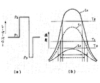
このLIMDOW媒体を用いて、安定に記録可能な充分な大きさの磁区をメモリ層に一旦形成し、その直後にこの磁区の後部を消去して微小磁区を形成する一連の動作について、図5に示した典型例を用いて説明する。
Hc> σw / (2Ms × h) (1)
FIG. 5 shows a series of operations in which a magnetic domain having a sufficiently large size that can be stably recorded is once formed in the memory layer by using this LIMDOW medium, and the rear part of the magnetic domain is erased immediately thereafter to form a micro magnetic domain. This will be described using the typical example shown.
図5(a)は記録レーザの駆動波形の一例であり、図5(b)はそれによりメモリ層に形成される磁区の模式図である。また、図5(a)中に記載のレーザパワーPw及びPeを照射したときに形成される記録膜面上の温度分布を、それぞれ図6に記載の温度分布(w)及び温度分布(e)で示す。また、レーザパワーPeを照射する直前の温度分布を、図6に記載の温度分布(i)で示す。以下に、図5(a)のようにレーザを駆動した時に、図の先頭のパワーレベルPwのパルスが照射された後、レーザ停止期間τを経て、パワーレベルPeのレーザが照射されるまでの間に、記録膜で起こる現象のプロセスを説明する。 FIG. 5A is an example of the drive waveform of the recording laser, and FIG. 5B is a schematic diagram of magnetic domains formed in the memory layer thereby. Further, the temperature distribution on the surface of the recording film formed when the laser powers Pw and Pe described in FIG. 5A are irradiated are the temperature distribution (w) and temperature distribution (e) shown in FIG. 6, respectively. It shows with. Further, the temperature distribution immediately before the laser power Pe is irradiated is indicated by a temperature distribution (i) shown in FIG. In the following, when the laser is driven as shown in FIG. 5A, after the pulse of the power level Pw at the top of the figure is irradiated, the laser of the power level Pe is irradiated after the laser stop period τ. In the meantime, a process of a phenomenon occurring in the recording film will be described.
Pwのレーザが照射されると、記録膜面上のスポットサイズ相応の領域がTw以上になる温度分布(w)が誘起され、レーザの照射が停止されると放熱による冷却が始まる。この冷却過程で、Tw以上に加熱された領域のW層が記録状態に配向し、続いてM層にその磁区が転写される。更に冷却が進むとW層の磁区の初期化が外周部から始まり、ピーク温度がTs以下になる温度分布(i)になると、W層は完全に初期化される。ここまでのプロセスが、次にパワーレベルPeのレーザが照射される直前までに完了する。この時点ではメモリ層には、図5(b)の先頭に示した円形状の磁区が形成されている。続いてパワーレベルPeのレーザが照射されると、スポットサイズ相応の領域がTm以上になる温度分布(e)が誘起され、その領域内の磁区が消去される。パワーレベルPwのレーザが照射された時点から、次にパワーレベルPeのレーザが照射されるまでの間に媒体が移動した距離に応じて、消去領域は直前に記録した磁区よりも後方にシフトするので、図5(b)の波線で示した2番目の円形状の部分が消去され、前部に三日月状の微小磁区が残る。 When the Pw laser is irradiated, a temperature distribution (w) is induced in which the area corresponding to the spot size on the recording film surface is equal to or higher than Tw, and when the laser irradiation is stopped, cooling by heat radiation starts. In this cooling process, the W layer in the region heated to Tw or more is oriented in the recording state, and then the magnetic domain is transferred to the M layer. When the cooling further proceeds, the initialization of the magnetic domain of the W layer starts from the outer periphery, and when the temperature distribution (i) at which the peak temperature is Ts or less is reached, the W layer is completely initialized. The process so far is completed immediately before the next irradiation with the laser of the power level Pe. At this time, the circular magnetic domain shown at the top of FIG. 5B is formed in the memory layer. Subsequently, when the laser of the power level Pe is irradiated, a temperature distribution (e) in which the region corresponding to the spot size becomes Tm or more is induced, and the magnetic domain in the region is erased. The erasure area shifts backward from the previously recorded magnetic domain in accordance with the distance the medium has moved between the time when the laser of the power level Pw is irradiated and the time when the laser of the power level Pe is irradiated next. Therefore, the second circular portion indicated by the wavy line in FIG. 5B is erased, and a crescent-shaped minute magnetic domain remains in the front portion.
最終的に形成される磁区の長さ及び消去領域の長さは、図5に示したようにPw及びPeの照射期間に対応させて任意に決めることが出来る。このようにして、スポット径に比して微細な記録マークを含む高密度記録パターンを光変調方式で記録することが可能になる。 これらの様に、交換結合多層膜を利用し、初期化磁界Hiを無くした光変調ダイレクトオーバーライト媒体が種々開発されているが、依然として、記録プロセスの際に記録磁界Hwの印加が必要であるという問題が残されている。 The length of the finally formed magnetic domain and the length of the erase region can be arbitrarily determined according to the irradiation periods of Pw and Pe as shown in FIG. In this way, it is possible to record a high-density recording pattern including a recording mark finer than the spot diameter by the light modulation method. As described above, various light modulation direct overwrite media using an exchange coupling multilayer film and eliminating the initialization magnetic field Hi have been developed. However, it is still necessary to apply the recording magnetic field Hw during the recording process. The problem remains.
これに対し、特開平10−134431号公報には、書き込み層を室温からキュリー温度の間に磁気的補償点を持たない希土類金属副格子磁化優勢な組成とし、記録プロセスにおいて、磁気的補償点を越え遷移金属副格子磁化優勢となっている初期化層とアンチパラレルの磁化状態を作り出すことで、記録磁界が無くても初期化層からの漏洩磁界を用いて書き込み層に磁化反転を起こさせ、オーバーライトが可能である技術が開示されている。
しかし、特開平10−134431号公報に開示されたダイレクトオーバーライトは、記録プロセス温度領域における初期化層からの漏洩磁界の大きさを出来るだけ大きくするよう、初期化層の磁化が最大となる温度を書き込み層のキュリー温度近傍に設ける必要があるため、初期化層の組成設計に制約が生じてしまう。更には、高温において磁化が大きいことで、初期化層が磁化反転を起こし易くなり、記録パワーマージンや耐久性の点で問題が生じてしまう場合がある。 However, the direct overwrite disclosed in Japanese Patent Laid-Open No. 10-134431 is a temperature at which the magnetization of the initialization layer is maximized so that the magnitude of the leakage magnetic field from the initialization layer in the recording process temperature region is as large as possible. Must be provided in the vicinity of the Curie temperature of the writing layer, which restricts the composition design of the initialization layer. Furthermore, since the magnetization is large at a high temperature, the initialization layer is likely to cause magnetization reversal, which may cause problems in terms of recording power margin and durability.
また、書き込み層においても、記録プロセス温度領域において遷移金属副格子磁化優勢となっている初期化層とアンチパラレルの磁化状態とする必要があるため、室温からキュリー温度の間に磁気的補償点を持たない希土類金属副格子磁化優勢な組成とする必要があり、組成設計に制約が生じてしまう。更には、書き込み層の保磁力を初期化層からの漏洩磁界よりも小さくする必要があるため、記録磁区の形状保存安定性に欠ける結果となり、ジッター特性や信号欠落率が悪化してしまうといった問題が生じてしまう場合がある。 In addition, since the write layer also needs to be in an anti-parallel magnetization state with the initialization layer that is transition metal sublattice magnetization dominant in the recording process temperature region, a magnetic compensation point is set between the room temperature and the Curie temperature. It is necessary to use a rare earth metal sublattice magnetization dominant composition that does not have, thus limiting the composition design. Furthermore, since the coercive force of the writing layer needs to be smaller than the leakage magnetic field from the initialization layer, it results in a lack of recording stability of the recording magnetic domain, and the jitter characteristics and signal loss rate deteriorate. May occur.
本発明はかかる問題点に鑑みてなされたものであり、外部記録磁界Hwを印加しなくても、スポット径に比して微細な高密度記録パターンを安定に光変調方式でダイレクトオーバーライト記録できる光学的記録媒体を提供することを目的とする。 The present invention has been made in view of such problems, and can directly and directly record a direct recording by a light modulation method with a high-density recording pattern finer than the spot diameter without applying an external recording magnetic field Hw. An object is to provide an optical recording medium.
上記目的は以下の光学的記録媒体により達成される。 The above object is achieved by the following optical recording medium.
少なくともメモリ層、書き込み層、遮断層、及び初期化層を有し、第1の照射パルスにより一定長の記録領域を形成した後、情報に対応した走査距離を経て、第2の照射パルスにより前記形成された記録領域の後部を消去することにより、情報に応じた複数の長さの記録マークを光変調オーバーライト記録する情報記録方法に用いられる光学的記録媒体において、
前記初期化層上に、前記書き込み層に対して漏洩磁界を発生させる垂直磁化膜から成る記録磁界層と、該記録磁界層の磁化を交換結合により膜面内方向に配向させる磁性膜から成る面内磁化誘導層と、前記面内磁化誘導層と前記記録磁界層との間に、室温において交換結合し、かつ、前記面内磁化誘導層および前記記録磁界層よりもキュリー温度の低い磁性層から成る第二遮断層とが積層されていることを特徴とする光学的記録媒体。
It has at least a memory layer, a writing layer, a blocking layer, and an initialization layer, and after forming a recording area of a certain length by the first irradiation pulse, after passing a scanning distance corresponding to information, the second irradiation pulse In an optical recording medium used in an information recording method for performing light modulation overwrite recording of a plurality of lengths of recording marks according to information by erasing the rear portion of the formed recording area,
A recording magnetic layer made of a perpendicular magnetic film that generates a leakage magnetic field on the write layer on the initialization layer, and a surface made of a magnetic film that orients the magnetization of the recording magnetic layer in the in-film direction by exchange coupling An internal magnetization induction layer, a magnetic layer that is exchange-coupled between the in-plane magnetization induction layer and the recording magnetic field layer at room temperature and has a Curie temperature lower than the in-plane magnetization induction layer and the recording magnetic field layer. An optical recording medium, wherein a second barrier layer is laminated.
本発明の構成を採る事により、スポット径よりも微細な高密度記録パターンを、初期化磁界Hiのみならず、記録磁界Hwを印加しなくても、安定に光変調方式でダイレクトオーバーライト記録可能な光学的記録媒体を提供することができる。 By adopting the configuration of the present invention, a high-density recording pattern that is finer than the spot diameter can be directly overwritten by the light modulation method stably without applying the recording magnetic field Hw as well as the initialization magnetic field Hi. An optical recording medium can be provided.
以下、本発明図面を参照して詳細に説明する。 Hereinafter, the present invention will be described in detail with reference to the drawings.
図1は、本発明による光学的記録媒体の一実施態様を示す模式的断面図である。この態様においては、基板1016上に、第一の誘電体層1013、再生層(D1)1001、再生補助層(D2)1002、制御層(C)1003、第三遮断層(Sr)1004、メモリ層(M)1005、中間層(Int)1006、書き込み層(W)1007、遮断層(Sw)1008、初期化層(I)1009、記録磁界層(Wh)1010、第二遮断層(Sh)1011、面内磁化誘導層(IP)1012、第二の誘電体層1014、及び放熱層1015が順次積層されている。 FIG. 1 is a schematic cross-sectional view showing an embodiment of an optical recording medium according to the present invention. In this embodiment, on a substrate 1016, a first dielectric layer 1013, a reproduction layer (D1) 1001, a reproduction auxiliary layer (D2) 1002, a control layer (C) 1003, a third blocking layer (Sr) 1004, a memory Layer (M) 1005, intermediate layer (Int) 1006, write layer (W) 1007, blocking layer (Sw) 1008, initialization layer (I) 1009, recording magnetic field layer (Wh) 1010, second blocking layer (Sh) 1011, an in-plane magnetization induction layer (IP) 1012, a second dielectric layer 1014, and a heat dissipation layer 1015 are sequentially stacked.
再生層1001からメモリ層1005(D1/D2/C/Sr/M)の部分がDWDDによる再生を実現するための層構成であり、メモリ層1005から初期化層1009(M/Int/W/Sw/I)の部分がLIMDOWによる記録を実現するための層構成であり、記録磁界層1010から面内磁化誘導層1012(Wh/Sh/IP)の部分が記録領域の形成プロセスにおいて書き込み層に対して漏洩磁界を発生させるための層構成である。
A portion from the reproduction layer 1001 to the memory layer 1005 (D1 / D2 / C / Sr / M) has a layer configuration for realizing reproduction by DWDD. The
層間の交換結合のオン・オフを切り換える機能を果たす遮断層が、DWDDとLIMDOWの両方の構成に存在するので、区別のために前者の遮断層をSr層、後者のそれをSwおよびSh層と示してある。 Since a barrier layer that functions to switch on / off of the exchange coupling between the layers exists in both the DWDD and LIMDOW configurations, the former barrier layer is referred to as the Sr layer, and the latter as the Sw and Sh layers for distinction. It is shown.
基板1016としては、例えば、ポリカーボネート、アクリル、ガラス等を用いることができる。第一の誘電体層1013や第二の誘電体層1014としては、例えば、SiN、AlN、SiO、ZnS、MgF、TaO等の材料が使用できる。また、磁壁の移動を光学的に検出するのでなければ、必ずしも透光性材料である必要はない。 As the substrate 1016, for example, polycarbonate, acrylic, glass, or the like can be used. As the first dielectric layer 1013 and the second dielectric layer 1014, for example, materials such as SiN, AlN, SiO, ZnS, MgF, and TaO can be used. Further, unless the movement of the domain wall is optically detected, it is not always necessary to use a translucent material.
本実施の形態では、再生特性向上の観点から再生補助層1002を設け再生温度範囲で再生層全体における飽和磁化がキャンセルされるようにして、磁壁移動動作に及ぼす浮遊磁界の影響を抑制した場合の例を示してあるが、これ以外に膜厚方向に組成勾配を設ける、或いは、更に多層化した構成を用いても良い。材料としては、GdFeCo、GdDyFeCo系から成る磁性膜を用いることができる。
また、制御層1003は、再生ビームスポット内後方端部での余計な磁壁移動(ゴースト信号)を抑制するものであり、TbFeCo、TbDyFeCo系から成る磁性層などを用いることができる。
In the present embodiment, when the reproduction auxiliary layer 1002 is provided from the viewpoint of improving reproduction characteristics so that saturation magnetization in the entire reproduction layer is canceled in the reproduction temperature range, the influence of the stray magnetic field on the domain wall motion is suppressed. Although an example is shown, in addition to this, a composition gradient may be provided in the film thickness direction, or a multilayered structure may be used. As a material, a magnetic film made of GdFeCo or GdDyFeCo can be used.
The control layer 1003 suppresses extra domain wall motion (ghost signal) at the rear end in the reproduction beam spot, and a magnetic layer made of TbFeCo, TbDyFeCo, or the like can be used.
また、中間層(Int)1006は、メモリ層1005と書き込み層1007との間の交換相互作用の強さを調整するためのものであり、GdFeCo系から成る磁性層を用いることが出来る。
The intermediate layer (Int) 1006 is for adjusting the strength of exchange interaction between the
記録磁界層1010は、記録領域を形成するプロセスにおいて書き込み層1007に対して漏洩磁界を発生させるための層であり、GdFeCo、GdDyFeCo系からなる磁性膜を用いることができる。膜面内磁化誘導層1012は、前記記録磁界層1010を交換相互作用により膜面内方向に配向させるためのものであり、例えばCo元素を主成分とする磁性膜を用いることが出来るが、前記記録磁界層1010を交換相互作用により膜面内方向に配向させることができれば他の磁性膜を使うこともできる。また、第二遮断層1011は、前記記録磁界層1010と前記膜面内磁化誘導層1012との間の交換相互作用の効きを調整制御するためのものであり、前記記録磁界層1010と同じ材料GdFeCo、GdDyFeCo系からなる磁性膜を用いることができる。
The recording magnetic field layer 1010 is a layer for generating a leakage magnetic field with respect to the
また、放熱層1015としては、例えば、Al、AlTa、AlTi、AlCr、AlSi、Cu、Pt、Au等の材料が使用できる。 Further, as the heat dissipation layer 1015, for example, a material such as Al, AlTa, AlTi, AlCr, AlSi, Cu, Pt, or Au can be used.
また、高分子樹脂からなる保護コートを付与してもよい。あるいは、成膜後の基板を貼り合わせてもよい。また、磁性層以外の層は必須のものではなく、磁性層の積層順序を逆にしてもよい。 Moreover, you may provide the protective coat which consists of polymer resins. Alternatively, a substrate after film formation may be bonded. Further, layers other than the magnetic layer are not essential, and the stacking order of the magnetic layers may be reversed.
これら各層は、例えばマグネトロンスパッタ装置による連続スパッタリング、又は連続蒸着等によって被着形成できる。特に各磁性層は、真空を破ることなく連続成膜されることで、お互いに交換結合をしている。 Each of these layers can be deposited by, for example, continuous sputtering using a magnetron sputtering apparatus or continuous vapor deposition. In particular, the respective magnetic layers are exchange-coupled to each other by being continuously formed without breaking the vacuum.
上記媒体において、各磁性層1001〜1011は、磁気記録媒体や光磁気記録媒体に一般的に用いられている材料の他、磁気バブル材料や反強磁性材料等、種々の磁性材料によって構成することが考えられる。例えば、Pr、Nd、Sm、Eu、Gd、Tb、Dy、Ho、Er等の希土類金属元素の一種類あるいは二種類以上が10〜40原子%と、Fe、Co、Ni等の鉄族元素の一種類あるいは二種類以上が90〜60原子%とで構成される希土類−鉄族非晶質合金によって構成し得る。 In the above medium, each of the magnetic layers 1001 to 1011 is made of various magnetic materials such as a magnetic bubble material and an antiferromagnetic material in addition to materials generally used for magnetic recording media and magneto-optical recording media. Can be considered. For example, one or more rare earth metal elements such as Pr, Nd, Sm, Eu, Gd, Tb, Dy, Ho, Er, etc. are 10 to 40 atomic%, and iron group elements such as Fe, Co, Ni, etc. One kind or two or more kinds may be composed of a rare earth-iron group amorphous alloy composed of 90 to 60 atomic%.
また、耐食性向上等のために、これらの合金にCr、Mn、Cu、Ti、Al、Si、Pt、In等の元素を少量添加してもよい。また、Pt/Co、Pd/Co等の白金族−鉄族周期構造膜や、白金族−鉄族合金膜、Co−Ni−OやFe−Rh系合金等の反強磁性材料、磁性ガーネット等の材料も使用可能である。 In order to improve the corrosion resistance, a small amount of elements such as Cr, Mn, Cu, Ti, Al, Si, Pt, and In may be added to these alloys. Also, platinum group-iron group periodic structure films such as Pt / Co and Pd / Co, platinum group-iron group alloy films, antiferromagnetic materials such as Co-Ni-O and Fe-Rh alloys, magnetic garnet, etc. These materials can also be used.
重希土類−鉄族非晶質合金の場合、飽和磁化は、希土類元素と鉄族元素との組成比により制御することが可能である。補償組成にすれば、室温での飽和磁化を0emu/ccにできる。キュリー温度も、組成比により制御することが可能である。飽和磁化と独立に制御するためには、鉄族元素として、Feの一部をCoで置き換えた材料を用い、置換量を制御する方法がより好ましく利用できる。すなわち、Fe元素1原子%をCoで置換することにより、6℃程度のキュリー温度上昇が見込めるので、この関係を用いて所望のキュリー温度となるようにCoの添加量を調整する。Cr、Ti、Al等の非磁性元素を微量添加することにより、逆にキュリー温度を低下させることも可能である。また、二種類以上の希土類元素を用いてそれらの組成比を調整することでもキュリー温度を制御できる。 In the case of a heavy rare earth-iron group amorphous alloy, the saturation magnetization can be controlled by the composition ratio of the rare earth element and the iron group element. If the compensation composition is used, the saturation magnetization at room temperature can be 0 emu / cc. The Curie temperature can also be controlled by the composition ratio. In order to control independently of the saturation magnetization, a method of using a material in which part of Fe is replaced with Co as an iron group element and controlling the amount of substitution can be used more preferably. That is, by replacing 1 atomic% of the Fe element with Co, a Curie temperature rise of about 6 ° C. can be expected. Therefore, using this relationship, the amount of Co added is adjusted so as to obtain a desired Curie temperature. Conversely, the Curie temperature can be lowered by adding a small amount of a nonmagnetic element such as Cr, Ti, or Al. The Curie temperature can also be controlled by adjusting the composition ratio of two or more rare earth elements.
各磁性層のキュリー温度の設計において、DTE方式のプロセスを実現させる上で特に注意すべき点は、記録・消去・初期化の各温度に関わる磁性層、即ちW層・M層・Sw層のキュリー温度の設計である。記録温度まで加熱後、瞬時に初期化温度まで冷却して初期化を行い、直後に消去温度まで加熱するので、各温度の差は出来るだけ小さい方がよい。 In designing the Curie temperature of each magnetic layer, the points to be particularly noted in realizing the DTE process are the magnetic layers related to the recording, erasing and initialization temperatures, that is, the W layer, M layer, and Sw layer. Curie temperature design. After heating to the recording temperature, the temperature is instantly cooled to the initialization temperature, initialization is performed, and immediately after that, the temperature is heated to the erasing temperature. Therefore, the difference between the temperatures should be as small as possible.
通常のLIMDOW媒体では、消去温度レベルの温度分布を形成した時に、分布のピーク温度が記録温度を越えてはならないので、記録温度と消去温度との差を大きく取る必要があった。しかし、DTE方式の場合には、消去動作を行った時に中心の高温部に磁区が書けてしまっても、後続の記録もしくは消去の動作で上書きするようにできるので問題がない。このためM層のキュリー温度をW層のキュリー温度近くの高温に設計することが出来る。本実施例では両者の差が50℃以下になるようにした。またそれに伴って、Sw層のキュリー温度も、W層の初期化がM層の磁化状態に影響を及ぼさない範囲で、M層のキュリー温度近くの高温に設計することが出来る。本実施例ではW層とSw層とのキュリー温度の差を100℃以下に抑制した。 In a normal LIMDOW medium, when the temperature distribution of the erasing temperature level is formed, the peak temperature of the distribution must not exceed the recording temperature, so it is necessary to take a large difference between the recording temperature and the erasing temperature. However, in the case of the DTE method, even if a magnetic domain can be written in the central high temperature part when performing the erasing operation, there is no problem because it can be overwritten by the subsequent recording or erasing operation. For this reason, the Curie temperature of the M layer can be designed to be a high temperature close to the Curie temperature of the W layer. In this example, the difference between the two was set to 50 ° C. or less. Along with this, the Curie temperature of the Sw layer can also be designed at a high temperature close to the Curie temperature of the M layer in a range where the initialization of the W layer does not affect the magnetization state of the M layer. In this example, the difference in Curie temperature between the W layer and the Sw layer was suppressed to 100 ° C. or less.
また、磁壁抗磁力や磁壁エネルギー密度は、主として材料元素の選択によって制御するが、下引きされる第一の誘電体層の状態や、スパッタガス圧等の成膜条件によっても調整可能である。TbやDy系の材料は異方性が大きく磁壁抗磁力や磁壁エネルギー密度が大きく、Gd系材料は小さい。不純物の添加等によってこれらの物性値を制御することもできる。膜厚は、成膜速度と成膜時間で制御できる。 Further, the domain wall coercive force and the domain wall energy density are controlled mainly by selection of material elements, but can also be adjusted by the state of the first dielectric layer to be subtracted and the film forming conditions such as sputtering gas pressure. Tb and Dy-based materials have large anisotropy and large domain wall coercive force and domain wall energy density, while Gd-based materials are small. These physical property values can also be controlled by adding impurities or the like. The film thickness can be controlled by the film formation speed and the film formation time.
なお、磁壁移動動作のレーザために、第二の誘電体層1014を成膜した後、一旦成膜装置から取り出して、記録トラックの両側を高出力のレーザでアニール処理している。また、成膜後に永久磁石で15kOe程度の磁界を印加してI層を全面初期化している。生産性を考慮する場合には、アニール時に同時に初期化を行うことも可能である。あるいは、基板の表面形状や成膜条件を適切化して、アニール処理を省略することも可能である。 In order to perform the domain wall motion laser, after the second dielectric layer 1014 is formed, the second dielectric layer 1014 is once taken out from the film forming apparatus, and both sides of the recording track are annealed with a high-power laser. In addition, the entire I layer is initialized by applying a magnetic field of about 15 kOe with a permanent magnet after film formation. When considering productivity, it is also possible to perform initialization simultaneously with annealing. Alternatively, the annealing process can be omitted by optimizing the surface shape of the substrate and the film forming conditions.
以下に具体的な実施例をもって本発明を詳細に説明するが、本発明はその主旨を逸脱しない限り、以下の実施例に限定されるものではない。 Hereinafter, the present invention will be described in detail with specific examples, but the present invention is not limited to the following examples without departing from the gist thereof.
(実施例1)
直流マグネトロンスパッタリング装置に、BドープしたSi、及びGd、Tb、FeCr、CoCrの各ターゲットを取り付け、トラッキング用の案内溝の形成されたポリカーボネート基板を基板ホルダーに固定した後、2×10⁻⁵Pa以下の高真空になるまでチャンバー内をクライオポンプで真空排気した。その後、真空排気したままArガスをチャンバー内に導入し、基板を回転させながら、ターゲットをスパッタして各層を成膜した。SiN層成膜時にはArガスに加えてN2ガスを導入することで、直流反応性スパッタを行い成膜した。
(Example 1)
After attaching B-doped Si and Gd, Tb, FeCr, and CoCr targets to a DC magnetron sputtering apparatus and fixing a polycarbonate substrate on which a tracking guide groove is formed to a substrate holder, 2 × 10 −5 Pa or less The chamber was evacuated with a cryopump until a high vacuum was achieved. Thereafter, Ar gas was introduced into the chamber while being evacuated, and each layer was formed by sputtering the target while rotating the substrate. At the time of forming the SiN layer, direct current reactive sputtering was performed by introducing
まず初に、ArガスとN2ガスをチャンバー内に流しコンダクタンス調整により圧力を所望の値とし、第一の誘電体層としてSiN層を35nm成膜した。磁性膜の成膜時にN2ガスが混入していると窒化などを起こし磁気特性に影響を与えるため、誘電体層とその他の磁性層は別のチャンバーにて成膜を行った。 First, Ar gas and N2 gas were flowed into the chamber, the pressure was adjusted to a desired value by conductance adjustment, and a SiN layer of 35 nm was formed as the first dielectric layer. When N2 gas is mixed during the formation of the magnetic film, nitriding occurs and affects the magnetic characteristics. Therefore, the dielectric layer and the other magnetic layers were formed in separate chambers.
第一の誘電体層成膜後に、別のチャンバーに基板を搬送しArガスを導入し、コンダクタンス調整により所望の圧力とし、再生層及び再生補助層として組成比の異なるGdFeCoCr層を各々膜厚18nm成膜した。次いで、Arガスを50sccmチャンバー内に導入し、コンダクタンスの調整により圧力を約1.0Paとし、制御層としてTbFeCoCrを膜厚18nm、第三遮断層としてTbFeCr層を膜厚10nm形成した。次いで、メモリ層としてTbFeCoCr層を膜厚50nm形成した。 After film formation of the first dielectric layer, the substrate is transported to another chamber, Ar gas is introduced, a desired pressure is obtained by adjusting conductance, and GdFeCoCr layers having different composition ratios as the reproduction layer and the reproduction auxiliary layer are each 18 nm in thickness. A film was formed. Next, Ar gas was introduced into the 50 sccm chamber, the pressure was adjusted to about 1.0 Pa by adjusting the conductance, and a TbFeCoCr film having a thickness of 18 nm was formed as a control layer, and a TbFeCr layer having a thickness of 10 nm was formed as a third blocking layer. Next, a TbFeCoCr layer having a thickness of 50 nm was formed as a memory layer.
その後、Arガスを35sccmチャンバー内に導入し、コンダクタンスの調整により圧力を0.7Paとし、中間層としてGdFeCoCrを膜厚30nm形成した。次いで、Arガスを10sccmチャンバー内に導入し、コンダクタンスの調整により圧力を約0.2Paとし、書き込み層としてTbFeCoCrを膜厚20nm形成した。書き込み層としては、DyFeCoCr系の使用も可能であるが、スパッタリング装置へのターゲット配置個数の関係から本発明ではTbFeCoCrを用い、成膜圧力を下げることで磁気異方性の調整を行った。 Thereafter, Ar gas was introduced into the 35 sccm chamber, the pressure was set to 0.7 Pa by adjusting the conductance, and GdFeCoCr was formed to a thickness of 30 nm as an intermediate layer. Next, Ar gas was introduced into the 10 sccm chamber, the pressure was adjusted to about 0.2 Pa by adjusting the conductance, and a TbFeCoCr film having a thickness of 20 nm was formed as the writing layer. As the writing layer, a DyFeCoCr-based material can be used. However, in the present invention, TbFeCoCr is used in the present invention, and the magnetic anisotropy is adjusted by lowering the film-forming pressure because of the number of targets arranged in the sputtering apparatus.
次いで、Arガスを50sccmチャンバー内に導入し、コンダクタンスの調整により圧力を1.0Paとし、遮断層としてTbFeCoCr層を膜厚10nm、初期化層としてTbFeCoCr層を膜厚30nm順次成膜した。 Next, Ar gas was introduced into the 50 sccm chamber, the pressure was adjusted to 1.0 Pa by adjusting the conductance, a TbFeCoCr layer having a thickness of 10 nm was formed as a blocking layer, and a TbFeCoCr layer having a thickness of 30 nm was sequentially formed as an initialization layer.
その後、記録磁界層および第二遮断層として組成比の異なるGdFeCoCr層を膜厚17nmと5nm、膜面内磁化誘導層としてCoCr層を膜厚3nm、Arガスを用いて成膜した。 After that, GdFeCoCr layers having different composition ratios as the recording magnetic field layer and the second blocking layer were formed with a film thickness of 17 nm and 5 nm, and a CoCr layer as the in-plane magnetization inducing layer was formed with a film thickness of 3 nm using Ar gas.
次いで、第二の誘電体層としてSiN層を20nm、第一の誘電体層形成時と同様直流反応性スパッタにより成膜した。 Next, a SiN layer was formed as a second dielectric layer to a thickness of 20 nm by direct current reactive sputtering in the same manner as the first dielectric layer was formed.
ここで、磁壁移動動作レーザのために、第二の誘電体層を成膜した後、一旦成膜装置から取り出して、記録トラックの両側を高出力のレーザで局所アニール処理を行った。この処理により、記録トラック両側の磁性膜の磁性を劣化させ、この部分では磁壁エネルギーが蓄積しないようにした。 Here, after the second dielectric layer was formed for the domain wall motion operation laser, it was once taken out from the film forming apparatus and subjected to local annealing treatment with a high-power laser on both sides of the recording track. This processing deteriorates the magnetic properties of the magnetic films on both sides of the recording track, so that domain wall energy is not accumulated in this portion.
その後、再び成膜装置に戻し、所望の圧力まで真空排気したのち、放熱層としてAlSi層を100nm、Arガスを用いて成膜した。 Thereafter, the film was returned to the film forming apparatus and evacuated to a desired pressure, and then an AlSi layer was formed as a heat dissipation layer using 100 nm and Ar gas.
各磁性層は、Gd、Tb、FeCr、CoCrの各ターゲットに投入するパワーの比によって組成比を制御した。DWDDによる再生を実現するための層構成(D1/D2/C/Sr/M)における組成比は、先にも述べた様に、再生特性向上の観点から再生温度範囲で磁壁移動動作に及ぼす浮遊磁界の影響を抑制するよう、各磁性層とも補償組成近傍の組成になるように調整した。厳密には、再生温度となる遮断層のキュリー温度近傍の温度で希土類元素と鉄族元素とが補償されるように、室温で希土類元素優勢になるように調整した。 The composition ratio of each magnetic layer was controlled by the ratio of power applied to each target of Gd, Tb, FeCr, and CoCr. As described above, the composition ratio in the layer structure (D1 / D2 / C / Sr / M) for realizing reproduction by DWDD has a floating effect on the domain wall motion operation in the reproduction temperature range from the viewpoint of improving reproduction characteristics. In order to suppress the influence of the magnetic field, each magnetic layer was adjusted to have a composition near the compensation composition. Strictly speaking, adjustment was made so that the rare earth element predominates at room temperature so that the rare earth element and the iron group element are compensated at a temperature in the vicinity of the Curie temperature of the blocking layer, which is the regeneration temperature.
具体的には、再生層のキュリー温度は290℃程度となるように調整し、再生補助層のキュリー温度は210℃程度、制御層のキュリー温度は180℃程度、第三遮断層のキュリー温度は160℃程度、メモリ層のキュリー温度は280℃程度、中間層のキュリー温度は310℃程度、書き込み層のキュリー温度は320℃程度、遮断層のキュリー温度は230℃程度、初期化層のキュリー温度は、400℃程度となる様に調整した。また、記録磁界層のキュリー温度は380℃程度、第二遮断層のキュリー温度は240℃程度となるように調整した。膜面磁化誘導層のキュリー温度は未測定であるが、一般的にCo膜のキュリー温度は1,500℃程度と言われており、それにCr元素等を微量添加した場合はCr元素1原子%で6℃程度のキュリー温度低下が見込まれる。本実施例ではCr元素を2.5原子%添加しているので、約15℃のキュリー温度低下が見込まれる。 Specifically, the Curie temperature of the regeneration layer is adjusted to be about 290 ° C., the Curie temperature of the regeneration auxiliary layer is about 210 ° C., the Curie temperature of the control layer is about 180 ° C., and the Curie temperature of the third blocking layer is About 160 ° C, Curie temperature of the memory layer is about 280 ° C, Curie temperature of the intermediate layer is about 310 ° C, Curie temperature of the writing layer is about 320 ° C, Curie temperature of the blocking layer is about 230 ° C, Curie temperature of the initialization layer Was adjusted to about 400 ° C. The Curie temperature of the recording magnetic layer was adjusted to about 380 ° C., and the Curie temperature of the second blocking layer was adjusted to about 240 ° C. Although the Curie temperature of the film surface magnetization induction layer has not been measured, it is generally said that the Co film has a Curie temperature of about 1,500 ° C. When a small amount of Cr element or the like is added thereto, 1 atomic% of Cr element is added. A decrease in Curie temperature of about 6 ° C is expected. In this embodiment, since 2.5 atomic% of Cr element is added, a Curie temperature drop of about 15 ° C. is expected.
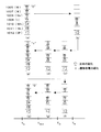
また記録磁界層(Wh)1010は、書き込み層(W)1007のキュリー温度近傍において、初期化層(I)1009とアンチパラレルの磁化状態をとる必要があるため、その磁気的補償温度をW層のキュリー温度近傍、若しくはそれ以上とすることが好ましい。図4を用いて詳細に説明する。 The recording magnetic layer (Wh) 1010 needs to be in an anti-parallel magnetization state with the initialization layer (I) 1009 in the vicinity of the Curie temperature of the write layer (W) 1007. It is preferable that the temperature be near the Curie temperature or higher. This will be described in detail with reference to FIG.
図4はLIMDOWプロセスに関与する部分、メモリ層(M)1005から面内磁化誘導層(IP)1012までの磁化状態を示し(但し、中間層は図示せず)、横軸は温度を示す。 FIG. 4 shows the magnetization state from the memory layer (M) 1005 to the in-plane magnetization inducing layer (IP) 1012 involved in the LIMDOW process (however, the intermediate layer is not shown), and the horizontal axis shows the temperature.
このような媒体を用いた光変調オーバーライトでは、情報に応じて光ビームの強度を変調することにより情報を記録する。すなわち、記録レーザ光の変調によって、レーザ照射部の媒体温度を、W層のキュリー温度Tw以上でかつI層のキュリー温度Ti以下の温度レベルと、M層のキュリー温度Tm以上でかつW層のキュリー温度Tw以下の温度レベルと、の2種類の温度レベルの間で変調し、以下に述べるように各々の温度レベルに対応させてM層の磁化を配向させることでオーバーライトを実現する。 In the light modulation overwrite using such a medium, information is recorded by modulating the intensity of the light beam according to the information. That is, by modulating the recording laser beam, the medium temperature of the laser irradiation part is set to a temperature level that is equal to or higher than the Curie temperature Tw of the W layer and equal to or lower than the Curie temperature Ti of the I layer, and is equal to or higher than the Curie temperature Tm of the M layer. Overwriting is realized by modulating between two temperature levels, the Curie temperature Tw or lower, and orienting the magnetization of the M layer according to each temperature level as described below.
以下では、Twに加熱した時にM層に形成される磁化状態を記録状態“1”とし、Tmに加熱した時に形成される磁化状態を消去状態“0”とする。I層は全面消去状態に初期化着磁されており、キュリー温度が最も高く、上記の温度レベルへの加熱操作では磁化反転することなく常に消去状態を維持する。 Hereinafter, the magnetization state formed in the M layer when heated to Tw is referred to as a recording state “1”, and the magnetization state formed when heated to Tm is referred to as an erased state “0”. The I layer is initialized and magnetized to the entire erased state, has the highest Curie temperature, and always maintains the erased state without reversal of magnetization in the heating operation to the above temperature level.
まず、記録プロセスについて説明する。レーザ照射により、W層のキュリー温度Tw以上でかつI層のキュリー温度Ti以下の温度レベルに媒体が加熱され、W層の磁化が消失する(状態(b))。この際、第二遮断層(Sh)1011もキュリー温度を超え磁化が消失しているため、Wh層においては、Sh層を介したIP層との交換相互作用から解き放たれ、本来の姿である膜面垂直方向に磁化配向することとなる。 First, the recording process will be described. Laser irradiation heats the medium to a temperature level not lower than the Curie temperature Tw of the W layer and not higher than the Curie temperature Ti of the I layer, and the magnetization of the W layer disappears (state (b)). At this time, since the second blocking layer (Sh) 1011 also exceeds the Curie temperature and the magnetization has disappeared, the Wh layer is released from the exchange interaction with the IP layer via the Sh layer, and is in its original form. The magnetization is oriented in the direction perpendicular to the film surface.
その後の冷却過程で媒体温度がTw以下に低下すると、W層に磁化が芽生え初めてくるが、この時、Wh層からの漏洩磁界の作用によりW層の磁化が記録状態に配向する(状態(c))。 When the medium temperature falls below Tw in the subsequent cooling process, magnetization begins to develop in the W layer. At this time, the magnetization of the W layer is oriented to the recording state by the action of the leakage magnetic field from the Wh layer (state (c )).
ここで、本実施の形態では、上記プロセスにおいて、Wh層からの漏洩磁界の作用によりW層の磁化を記録状態に配向させる必要があるため、Wh層はI層とアンチパラレルである必要がある。また、出来るだけ漏洩磁界を大きくすることが望ましいため、Wh層のキュリー温度及び磁気的補償温度はTwよりも20℃以上高いことが好ましい。 Here, in the present embodiment, in the above process, it is necessary to orient the magnetization of the W layer in the recording state by the action of the leakage magnetic field from the Wh layer, so the Wh layer needs to be anti-parallel to the I layer. . Further, since it is desirable to make the leakage magnetic field as large as possible, it is preferable that the Curie temperature and the magnetic compensation temperature of the Wh layer be 20 ° C. or higher than Tw.
その後の冷却過程で更に媒体温度がTm以下に低下すると、W層との交換相互作用によりM層も記録状態に配向する(状態(d))。更にSw層のキュリー温度TSw以下に媒体温度が低下すると、Sw層を介してW層がI層と交換結合し、その作用によってW層が再反転して消去状態に初期化される。この時にはM層は媒体温度の低下に伴う保磁力エネルギーの急激な増大に支えられ、W層との交換相互作用に反して記録状態を維持する(状態(e))。 When the medium temperature is further lowered to Tm or lower in the subsequent cooling process, the M layer is also oriented in the recording state by exchange interaction with the W layer (state (d)). Further, when the medium temperature is lowered below the Curie temperature TSw of the Sw layer, the W layer is exchange-coupled with the I layer via the Sw layer, and the W layer is reinverted by the action and initialized to the erased state. At this time, the M layer is supported by a sudden increase in coercive energy accompanying a decrease in the medium temperature, and maintains the recording state against the exchange interaction with the W layer (state (e)).
次に消去プロセスを説明する。レーザ照射により媒体温度がTm以上でかつTw以下の温度レベルに加熱されると、W層はこの温度では保磁力エネルギーがまだ充分大きいので初期化された消去状態を維持し(状態(f))、M層はキュリー温度に加熱される過程で保磁力エネルギーが急激に低下するのでW層との交換相互作用により消去状態に配向する(状態(g))。 Next, the erasing process will be described. When the medium temperature is heated to a temperature level higher than Tm and lower than Tw by laser irradiation, the W layer maintains the erased state initialized (state (f)) because the coercive energy is still sufficiently large at this temperature. The M layer is orientated in an erased state by exchange interaction with the W layer because the coercive force energy rapidly decreases in the process of being heated to the Curie temperature (state (g)).
このようにして、2種類の温度レベルに対応してメモリ層を磁化配向させることができ、記録光の変調のみで記録前の磁化状態に関わらず新しい情報を記録することが可能となる。 In this manner, the memory layer can be magnetized and oriented corresponding to two kinds of temperature levels, and new information can be recorded by only modulating the recording light regardless of the magnetization state before recording.
こうして作製レーザ例1におけるサンプルの動特性評価を、従来から一般的に使用されているレーザ波長660nm、対物レンズのN.A.0.60の光磁気ディスク評価装置を用いて評価した。スポット径は約0.92μmである。録再時の線速は2.13m/secとした。 In this way, the dynamic characteristics of the sample in the manufactured laser example 1 were evaluated using a laser wavelength of 660 nm, which has been conventionally used, and an N.P. A. Evaluation was performed using a 0.60 magneto-optical disk evaluation apparatus. The spot diameter is about 0.92 μm. The linear velocity during recording / playback was 2.13 m / sec.
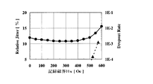
上記の光磁気記録媒体に、光学系の分解能以上の高密度な微細パターンを、DTE方式で記録し、このパターンをDWDD再生して特性評価を行った。具体的には、ジッターと信号欠落率の記録磁界依存性を(1−7)RLL変調における線記録密度80nm/bitの最短記録マーク長107nm(2Tトーン信号)について調べた。この際、パルス幅はduty25%に固定とした。結果を図2に示す。図中、●印が相対ジッターを表し、▲印がドロップアウトレートを表す。 On the above-mentioned magneto-optical recording medium, a fine pattern having a high density exceeding the resolution of the optical system was recorded by the DTE method, and this pattern was reproduced by DWDD to evaluate the characteristics. Specifically, the dependence of jitter and signal loss rate on the recording magnetic field was examined for the shortest recording mark length of 107 nm (2T tone signal) with a linear recording density of 80 nm / bit in (1-7) RLL modulation. At this time, the pulse width was fixed to 25% duty. The results are shown in FIG. In the figure, the mark ● represents the relative jitter, and the mark ▲ represents the dropout rate.
本実施例のサンプルでは、ジッターに関してビットエラーレート1×10⁻⁴以下に相当する値、相対ジッターで12.8%以下の値が記録磁界無しでも得られており、且つ、信号欠落率に関しても記録磁界無しで1×10⁻⁴以下のドロップアウトレートが得られており、非常に良好な結果であった。また、記録磁界500Oe以上で見られる特性悪化は、書き込み層から記録層への消去側の転写不良によるものと思われる。 In the sample of this example, a value corresponding to a bit error rate of 1 × 10 −4 or less with respect to jitter and a value of 12.8% or less in relative jitter were obtained without a recording magnetic field, and the signal loss rate was also related. A dropout rate of 1 × 10 −4 or less was obtained without a recording magnetic field, which was a very good result. Further, the characteristic deterioration observed at a recording magnetic field of 500 Oe or more is considered to be due to transfer failure on the erasure side from the writing layer to the recording layer.
また、本実施例においては前記記録磁界層の膜厚17nmに対して、前記第二遮断層を5nm、前記面内磁化誘導層を3nmとしたが、該第二遮断層に関しては膜厚20nm以下の範囲、該面内磁化誘導層に関しては膜厚15nm以下の範囲であれば、記録磁界無しにおいて、相対ジッターで約10.5%、且つ、1×10⁻⁵以下のドロップアウトレートが得られ、さらに良好であった。 In this embodiment, the second blocking layer is 5 nm and the in-plane magnetization inducing layer is 3 nm with respect to the recording magnetic layer thickness of 17 nm. The second blocking layer has a thickness of 20 nm or less. In the case of the in-plane magnetization inducing layer, if the film thickness is in the range of 15 nm or less, a dropout rate of about 10.5% relative jitter and 1 × 10 −5 or less can be obtained without a recording magnetic field. It was even better.
これら前記第二遮断層、および前記面内磁化誘導層の膜厚は、前記記録磁界層の膜厚に対しての設計事項であり、前記第二遮断層のキュリー温度近傍において、前記記録磁界層の磁化配向が膜面内方向から垂直方向に変化するように調整されるものである。 The film thickness of the second blocking layer and the in-plane magnetization inducing layer is a design matter with respect to the film thickness of the recording magnetic field layer, and the recording magnetic field layer is near the Curie temperature of the second blocking layer. The magnetization orientation is adjusted so as to change from the in-plane direction to the vertical direction.
また、前記記録磁界層、前記第二遮断層、および前記面内磁化誘導層においては、各層間は急峻明瞭である必要は無く、膜厚方向に組成勾配を設けることによって構成されても良い。
(比較例1)
前記記録磁界層、第二遮断層、面内磁化誘導層を形成しない以外は実施例1と同様にサンプルの作製、及び特性評価を行った。
In the recording magnetic field layer, the second blocking layer, and the in-plane magnetization inducing layer, each layer does not need to be sharp and clear, and may be configured by providing a composition gradient in the film thickness direction.
(Comparative Example 1)
Samples were prepared and characteristics were evaluated in the same manner as in Example 1 except that the recording magnetic field layer, the second blocking layer, and the in-plane magnetization inducing layer were not formed.
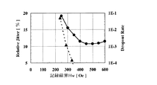
その結果、図3に示すように本比較例サンプルにおいては、ジッターと信号欠落率に関し記録磁界400から600Oeの範囲においてビットエラーレート1×10⁻⁴以下に相当する値が得られ、400Oe程度の記録磁界印加が必要であることが分かった。
As a result, as shown in FIG. 3, in this comparative example sample, a value corresponding to a bit error rate of 1 × 10 −4 or less is obtained in the range of the recording
1001 再生層
1002 再生補助層
1003 制御層
1004 第三遮断層
1005 メモリ層
1006 中間層
1007 書き込み層
1008 遮断層
1009 初期化層
1010 記録磁界層
1011 第二遮断層
1012 面内磁界誘導層
1013 第一の誘電体層
1014 第二の誘電体層
1015 放熱層
1016 基板
1001 reproduction layer 1002 reproduction auxiliary layer 1003 control layer 1004
Claims (1)
前記初期化層上に、前記書き込み層に対して漏洩磁界を発生させる垂直磁化膜から成る記録磁界層と、該記録磁界層の磁化を交換結合により膜面内方向に配向させる磁性膜から成る面内磁化誘導層と、前記面内磁化誘導層と前記記録磁界層との間に、室温において交換結合し、かつ、前記面内磁化誘導層および前記記録磁界層よりもキュリー温度の低い磁性層から成る第二遮断層とが積層されていることを特徴とする光学的記録媒体。 It has at least a memory layer, a writing layer, a blocking layer, and an initialization layer, and after forming a recording area of a certain length by the first irradiation pulse, after passing a scanning distance corresponding to information, the second irradiation pulse In an optical recording medium used in an information recording method for performing light modulation overwrite recording of a plurality of lengths of recording marks according to information by erasing the rear portion of the formed recording area,
A recording magnetic layer made of a perpendicular magnetic film that generates a leakage magnetic field on the write layer on the initialization layer, and a surface made of a magnetic film that orients the magnetization of the recording magnetic layer in the in-film direction by exchange coupling An internal magnetization induction layer, a magnetic layer that is exchange-coupled between the in-plane magnetization induction layer and the recording magnetic field layer at room temperature and has a Curie temperature lower than the in-plane magnetization induction layer and the recording magnetic field layer. An optical recording medium, wherein a second barrier layer is laminated.
Priority Applications (1)
| Application Number | Priority Date | Filing Date | Title |
|---|---|---|---|
| JP2004109960A JP2005293768A (en) | 2004-04-02 | 2004-04-02 | Optical recording medium |
Applications Claiming Priority (1)
| Application Number | Priority Date | Filing Date | Title |
|---|---|---|---|
| JP2004109960A JP2005293768A (en) | 2004-04-02 | 2004-04-02 | Optical recording medium |
Publications (1)
| Publication Number | Publication Date |
|---|---|
| JP2005293768A true JP2005293768A (en) | 2005-10-20 |
Family
ID=35326525
Family Applications (1)
| Application Number | Title | Priority Date | Filing Date |
|---|---|---|---|
| JP2004109960A Pending JP2005293768A (en) | 2004-04-02 | 2004-04-02 | Optical recording medium |
Country Status (1)
| Country | Link |
|---|---|
| JP (1) | JP2005293768A (en) |
Cited By (1)
| Publication number | Priority date | Publication date | Assignee | Title |
|---|---|---|---|---|
| WO2016021403A1 (en) * | 2014-08-07 | 2016-02-11 | 国立研究開発法人理化学研究所 | Storage medium, recording device, data processing device, data recording device, and communications device |
-
2004
- 2004-04-02 JP JP2004109960A patent/JP2005293768A/en active Pending
Cited By (2)
| Publication number | Priority date | Publication date | Assignee | Title |
|---|---|---|---|---|
| WO2016021403A1 (en) * | 2014-08-07 | 2016-02-11 | 国立研究開発法人理化学研究所 | Storage medium, recording device, data processing device, data recording device, and communications device |
| JPWO2016021403A1 (en) * | 2014-08-07 | 2017-06-01 | 国立研究開発法人理化学研究所 | Storage medium, recording device, data processing device, data recording device, and communication device |
Similar Documents
| Publication | Publication Date | Title |
|---|---|---|
| JP3647219B2 (en) | Method of reproducing signal from magnetic recording medium | |
| JP3332750B2 (en) | Magnetic recording medium, recording method, reproducing method, and method of manufacturing magnetic recording medium | |
| JP3416548B2 (en) | Magnetic recording medium, reproducing method and reproducing apparatus | |
| JPH10149592A (en) | Magneto-optical recording medium for reproducing information using domain wall motion and signal reproducing method | |
| JP2005293768A (en) | Optical recording medium | |
| US7522479B2 (en) | Domain wall displacement for magneto-optical recording medium having multiple magnetic layers | |
| US7210155B2 (en) | Magneto-optical recording medium having in-plane magnetizing layer | |
| JPH11328762A (en) | Magneto-optical recording medium | |
| US7173885B2 (en) | Domain-wall-displacement-type magnetooptical recording medium | |
| JP2003263806A (en) | Magneto-optical recording medium | |
| JP2002208193A (en) | Magneto-optical recording medium and information reproducing method therefor | |
| JP3977238B2 (en) | Magneto-optical recording medium | |
| JP3631194B2 (en) | Method for manufacturing magneto-optical recording medium | |
| JP2005302101A (en) | Optical recording medium | |
| JP3332913B2 (en) | Magnetic recording medium | |
| JP2000207791A (en) | Magnetic recording medium | |
| JP2003272262A (en) | Magneto-optical recording medium | |
| JP2006221768A (en) | Optical recording medium | |
| JP2006338717A (en) | optical disk | |
| JP2003303456A (en) | Magneto-optical recording medium and manufacturing method thereof | |
| JP3332905B2 (en) | Method and apparatus for reproducing magneto-optical recording medium | |
| JP2008152842A (en) | Magnetic recording medium | |
| JP2002157793A (en) | Magnetic recording medium | |
| JP2005056454A (en) | Magnetic recording medium | |
| JP2006221703A (en) | Magneto-optical recording medium |