JP2005293631A - Manufacturing method of stamper and manufacturing method of optical disk substrate - Google Patents
Manufacturing method of stamper and manufacturing method of optical disk substrate Download PDFInfo
- Publication number
- JP2005293631A JP2005293631A JP2004102837A JP2004102837A JP2005293631A JP 2005293631 A JP2005293631 A JP 2005293631A JP 2004102837 A JP2004102837 A JP 2004102837A JP 2004102837 A JP2004102837 A JP 2004102837A JP 2005293631 A JP2005293631 A JP 2005293631A
- Authority
- JP
- Japan
- Prior art keywords
- photoresist
- stamper
- optical disk
- manufacturing
- pit
- Prior art date
- Legal status (The legal status is an assumption and is not a legal conclusion. Google has not performed a legal analysis and makes no representation as to the accuracy of the status listed.)
- Pending
Links
Images
Landscapes
- Manufacturing Optical Record Carriers (AREA)
Abstract
Description
本発明は、スタンパの製造方法及び光ディスク基板の製造方法に用いられるフォトレジストに関するものである。 The present invention relates to a photoresist used in a stamper manufacturing method and an optical disk substrate manufacturing method.
光ディスクには、情報通信及び画像処理技術の急速な発展に伴い、更なる高密度記録が要求されている。DVD(ディジタル・バーサタイル・ディスク)よりも大きな記録容量を有した片面で25GBの記録容量を収納できる光ディスクの開発も行われている。このためには、光ディスクに記録されるピット長又はグルーブ長は、DVDの0.4μmから0.15μmへ、トラックピッチは、0.74μmから0.32μmへと大幅に小さくすることが要求される。 Optical disks are required to have higher density recording with rapid development of information communication and image processing technologies. Development of an optical disk capable of storing a recording capacity of 25 GB on one side having a larger recording capacity than that of a DVD (digital versatile disk) is also underway. For this purpose, the pit length or groove length recorded on the optical disc is required to be significantly reduced from 0.4 μm to 0.15 μm for DVD, and the track pitch from 0.74 μm to 0.32 μm. .
このような高密度でピットを形成するためにはレーザ波長の短波長化と対物レンズの開口数の高NA化が求められる。
しかし、対物レンズの開口数NAは、レンズ設計製作精度の面から0.9が限界である。露光波長266nmの遠紫外線レーザ光を用いてもピット長は0.23μmが限界である。
In order to form pits at such a high density, it is required to shorten the laser wavelength and increase the numerical aperture of the objective lens.
However, the numerical aperture NA of the objective lens is limited to 0.9 in terms of lens design and production accuracy. Even when a far ultraviolet laser beam having an exposure wavelength of 266 nm is used, the limit of the pit length is 0.23 μm.
この対策として、特許文献1に記載されている方法がある。
即ち、特許文献1には、円形状のガラス基板上にスピンコートにより化学増幅型フォトレジストを塗布し、波長266nmの遠紫外レーザ光をカッティング光源として、内周から外周に向かって、NAが0.9前後の対物レンズを介して0.25μm以下のスポットサイズで露光した後、90℃のベーキングを行って、露光部に発生したプロトン酸を活性化させ、触媒的反応により露光部のみアルカリ現像可能な化学構造に変化させ、次に、アルカリ現像液に浸漬して前記露光部のみを溶解させ、前記化学増幅型フォトレジスト上に最短ピット長が0.1〜0.3μmであり、トラックピッチが0.1〜0.5μmのピット又はグルーブ状パターンを形成し、更に、スパッタにより、前記ピット又はグルーブ状パターンが形成された前記化学増幅型フォトレジスト上にNi薄膜を形成した後、電鋳法により、前記Ni薄膜上にNiメッキして光ディスク用スタンパを作製することが記載されている。
That is, in
しかしながら、酸による触媒的反応を用いているため、雰囲気中に極微量の塩基性物質が存在するだけでも化学増幅型フォトレジストの感度は、低下するので、前記パターン形状や前記パターンプロファイルが変化してしまうといった問題があった。
また、25GBといった高密度光ディスク用のスタンパの作製の場合には、露光開始点と露光終了点では、2時間以上の露光時間の差があるので、温度、湿度等の環境変化による触媒反応への影響により、ピット又はグルーブ形状が変わってしまうといった問題があった。このように、化学増幅型フォトレジストを用いる場合には、周囲の環境条件(塩基性物質の濃度、温度や湿度等)の厳密な管理が必要とされ、フォトレジスト自体が高価である上に環境条件の整備のための初期投資やメンテナンス等を含めたランニングコストも高価なものとなっていた。
However, since a catalytic reaction with an acid is used, the sensitivity of a chemically amplified photoresist decreases even if a very small amount of basic substance is present in the atmosphere, so that the pattern shape and the pattern profile change. There was a problem such as.
In the case of producing a stamper for a high-density optical disk such as 25 GB, there is a difference in exposure time of 2 hours or more between the exposure start point and the exposure end point. There is a problem that the pit or groove shape changes due to the influence. Thus, when using chemically amplified photoresists, it is necessary to strictly control the surrounding environmental conditions (concentration of basic substances, temperature, humidity, etc.), the photoresist itself is expensive and the environment Running costs including initial investment for maintenance of conditions and maintenance were also expensive.
そこで、本発明は、環境条件の影響を受けず、かつ安価に極微細なピット又はグルーブが形成された高密度で大記録容量の光ディスクが得られるスタンパの製造方法及び光ディスク基板の製造方法を提供することを目的とする。 Accordingly, the present invention provides a stamper manufacturing method and an optical disk substrate manufacturing method capable of obtaining an optical disk having a high density and a large recording capacity that is not affected by environmental conditions and is formed with extremely fine pits or grooves at low cost. The purpose is to do.
本願発明の第1の発明は、基板上にフォトレジストを塗布した後、波長が180〜300nmの遠紫外レーザ光を用いて、前記フォトレジストの露光を行った後、現像を行って、ピット又はグルーブ状パターンを形成し、次に、前記ピット又はグルーブ状パターン上に金属薄膜を形成し、前記金属薄膜上に電解メッキを行ってスタンパを作製するスタンパの製造方法において、前記フォトレジストは、重量平均分子量が2000〜10000で、かつビニルフェノールとメチルメタクリレートの比が3/7〜7/3の共重合体にAパラメータが0.6〜1.5μm-1を有するナフトキノンジアジド置換化合物を含むことを特徴とするスタンパの製造方法を提供する。
前記Aパラメータは、以下のように表される。
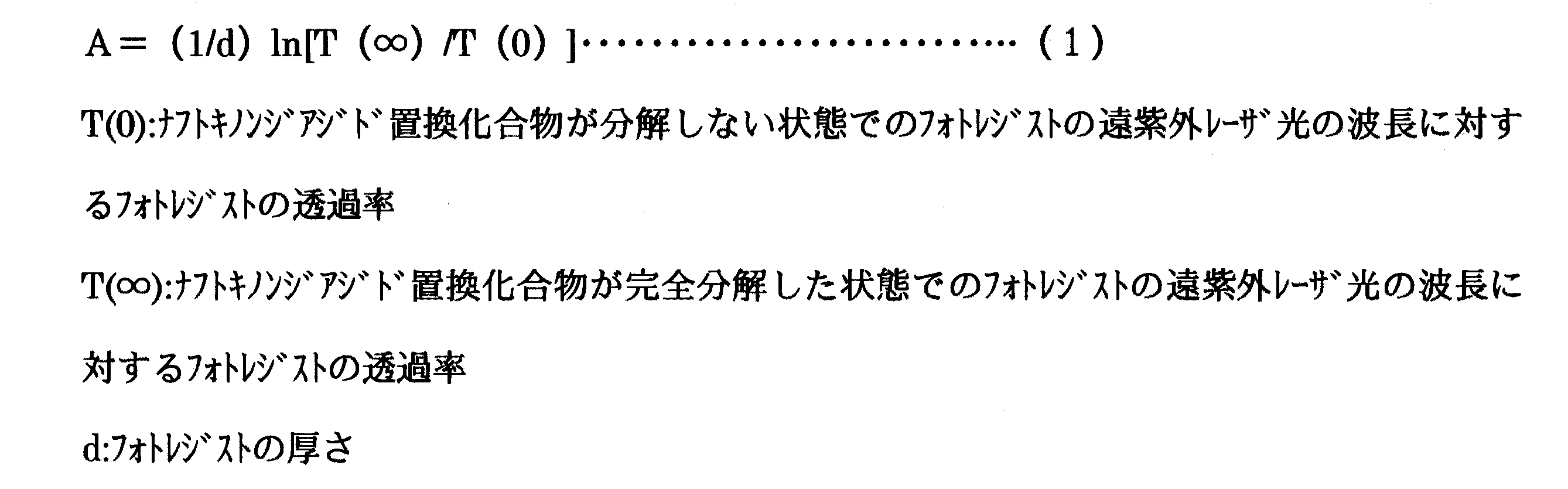
前記Aパラメータは、以下のように表される。
The A parameter is expressed as follows.
The A parameter is expressed as follows.
以上のように、本発明によれば、フォトレジストは、重量平均分子量が2000〜10000で、かつビニルフェノールとメチルメタクリレートの比が3/7〜7/3の共重合体にAパラメータが0.6〜1.5μm-1を有するナフトキノンジアジド置換化合物を含むので、環境条件の影響を受けず、かつ安価に極微細なピット又はグルーブが形成されたスタンパを得ることができる。また、このスタンパを用いた場合には、ピット又はグルーブを高密度にできるため、大記録容量の光ディスクを得ることができる。 As described above, according to the present invention, the photoresist has a weight average molecular weight of 2000 to 10000 and a copolymer having a vinylphenol / methyl methacrylate ratio of 3/7 to 7/3 has an A parameter of 0.00. Since it contains a naphthoquinonediazide substituted compound having 6 to 1.5 μm −1 , it is possible to obtain a stamper that is not affected by environmental conditions and that has ultrafine pits or grooves formed at low cost. Further, when this stamper is used, the pits or grooves can be made high density, so that an optical disk having a large recording capacity can be obtained.
本発明の実施の形態について図1を参照して説明する。
従来例を同一構成には、同一符号を付し、その説明を省略する。
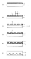
図1は、本発明の実施形態を示す製造工程断面図を示し、(A)は、フォトレジスト形成工程を示し、(B)は、潜像形成工程を示し、(C)は、凹凸状のパターン形成工程を示し、(D)は、Ni薄膜形成工程を示し、(E)は、スタンパ作製工程を示し、(F)は、光ディスク基板作製工程を示している。
An embodiment of the present invention will be described with reference to FIG.
The same reference numerals are given to the same configuration in the conventional example, and the description thereof is omitted.
FIG. 1 is a sectional view of a manufacturing process showing an embodiment of the present invention, (A) shows a photoresist forming process, (B) shows a latent image forming process, and (C) shows an uneven shape. The pattern formation process is shown, (D) shows the Ni thin film formation process, (E) shows the stamper production process, and (F) shows the optical disk substrate production process.
まずは、重量平均分子量5000を有するビニルフェノールとメチルアクリレートの共重合体を100部とベンゾフェノンの1,2−ナフトキノンジアジド−4−スルホン酸エステルを20部とプロピレングリコールモノメチルエーテルアセテートを4400部とを混合させ、孔径0.1μmのテトラフルオロエチレンフィルタ(ミリポア社製のテフロン(登録商標)フィルタ)で濾過して図1に示すフォトレジスト2を調剤する。ここで、ベンゾフェノンの1,2−ナフトキノンジアジド−4−スルホン酸エステルは、感光剤であり、プロピレングリコールモノメチルエーテルアセテートは、溶媒である。このベンゾフェノンの1,2−ナフトキノンジアジド−4−スルホン酸エステルは、ナフトキノンジアジド置換化合物の一種である。
First, 100 parts of a vinylphenol / methyl acrylate copolymer having a weight average molecular weight of 5000, 20 parts of 1,2-naphthoquinonediazide-4-sulfonic acid ester of benzophenone, and 4400 parts of propylene glycol monomethyl ether acetate are mixed. Then, it is filtered through a tetrafluoroethylene filter (Teflon (registered trademark) filter manufactured by Millipore) having a pore diameter of 0.1 μm to prepare a
このナフトキノンジアジド置換化合物としては、上記以外にベンゾフェノン系、ジフェニルスルボン系、ジフェニルメタン系等に代表される多価フェノール系の化合物、ポリビニルフェノールのような遠紫外領域で透明性の高い高分子化合物のヒドロキシル基をナフトキノンジアジドでエステル化した置換化合物がある。それ以外では、芳香族環の少ない構造、共役系の長さを調節し、吸収極大波長をずらす構造が推奨される。 Examples of the naphthoquinonediazide substituted compounds include polyphenolic compounds represented by benzophenone, diphenylsulfone, diphenylmethane, and the like, high-molecular compounds having high transparency in the far ultraviolet region, such as polyvinylphenol. There are substituted compounds in which the hydroxyl group is esterified with naphthoquinonediazide. Otherwise, a structure with few aromatic rings and a structure that adjusts the length of the conjugated system and shifts the absorption maximum wavelength are recommended.
次に、図1(A)に示すように、フォトレジスト2の密着性を良好にするために、ヘキサメチルジシラザンの蒸気中で直径200mm、厚さ10mmの円盤状のガラス基板1を3分間晒す。
引き続いて、図示しないスピンナー上にガラス基板1を載置し、回転時間を40秒、回転数を1000rpmで厚さ80nmのフォトレジスト2を塗布した後、80℃、45分間のベーキングを行って乾燥させる。
Next, as shown in FIG. 1A, in order to improve the adhesion of the
Subsequently, the
次に、図1(B)に示すように、フォトレジスト2の上方から波長266nmの遠紫外レーザ光を対物レンズ3を介して露光して、トラックピッチ0.32μm、最短ピット長0.149μmの潜像4を形成する。なお、最短ピット長が0.2μm以下の潜像4を形成するには、遠紫外レーザ光の波長は、180〜300nmの範囲内であれば可能である。
Next, as shown in FIG. 1B, a far-ultraviolet laser beam having a wavelength of 266 nm is exposed through the objective lens 3 from above the
次に、図1(C)に示すように、0.3N−OFPRディベロッパーNo.3(東京応化工業(株)製)を用いて、フォトレジスト2に形成された潜像4を60秒間現像した後、2分間の水洗を行って、凹凸状のピットパターン5を形成して光ディスク用原盤6を作製する。
Next, as shown in FIG. 3 (manufactured by Tokyo Ohka Kogyo Co., Ltd.) was used to develop the latent image 4 formed on the
次に、図1(D)に示すように、スパッタにより、光ディスク用原盤6の凹凸状のピットパターン5上にNi薄膜7を形成する。
更に、図1(E)に示すように、電鋳法により、Ni膜7上にNiメッキを行ってスタンパ8を作製する。
次に、図1(F)に示すように、スタンパ8を用いて、2P法等や射出成形により、トラックピッチ0.32μm、最短ピット長0.149μmの光ディスク基板9を作製する。更に、この光ディスク基板9上に反射層、記録層、保護層等を形成して光ディスクが得られる。
Next, as shown in FIG. 1D, a Ni thin film 7 is formed on the concave and convex pit patterns 5 of the optical disk master 6 by sputtering.
Further, as shown in FIG. 1E, a stamper 8 is produced by performing Ni plating on the Ni film 7 by electroforming.
Next, as shown in FIG. 1 (F), an optical disk substrate 9 having a track pitch of 0.32 μm and a shortest pit length of 0.149 μm is manufactured using a stamper 8 by the 2P method or the like or injection molding. Furthermore, an optical disk can be obtained by forming a reflective layer, a recording layer, a protective layer, and the like on the optical disk substrate 9.
ここで、ビニルフェノール(VP)とメチルメタクリレート(MMA)の共重合比(VP/MMA)を変化させたフォトレジスト2を用いて作製された光ディスクの試料1〜9のジッタ値について調べた。この際、前記遠紫外レーザ光照射の波長域において、フォトレジスト2のブリーチング特性を示すAパラメータは、1.0である。
上記したAパラメータは、(1)式で表される。
Here, the jitter values of
The above-mentioned A parameter is expressed by equation (1).
感光剤であるベンゾフェノンの1,2−ナフトキノンジアジド−4−スルホン酸エステルの濃度と関係し、感光剤濃度が大きいとフォトレジストの解像度が向上するが透過率は低下する。
このため、フォトレジストの解像度と遠紫外レーザ光のフォトレジストに対する透過率を考慮してベンゾフェノンの1,2−ナフトキノンジアジド−4−スルホン酸エステルの濃度を設定する必要がある。
This is related to the concentration of 1,2-naphthoquinonediazide-4-sulfonic acid ester of benzophenone, which is a photosensitizer. When the photosensitizer concentration is high, the resolution of the photoresist is improved, but the transmittance is lowered.
Therefore, it is necessary to set the concentration of 1,2-naphthoquinonediazide-4-sulfonic acid ester of benzophenone in consideration of the resolution of the photoresist and the transmittance of the far ultraviolet laser beam to the photoresist.
この時のビニルフェノールとメチルメタクリレートの共重合体の重量平均分子量は、5000である。フォトレジストは、ビニルフェノールとメチルメタクリレートの共重合体を100部と、ベンゾフェノンの1,2−ナフトキノンジアジド−4−スルホン酸エステルを20部、プロピレングリコールモノメチルエーテルアセテートを4400部により調剤されたものである。ジッタ値は、光ディスクの信号特性の品質を表す指標であり、7%以下であれば、良好な光ディスクであると判定される。このジッタ値の測定は、波長が405nmのレーザ光、対物レンズのNAが0.8の光ピックアップを用いて、リミットイコライジング後に行った。その結果を表1に示す。 The weight average molecular weight of the copolymer of vinylphenol and methyl methacrylate at this time is 5000. The photoresist was formulated with 100 parts of a copolymer of vinylphenol and methyl methacrylate, 20 parts of 1,2-naphthoquinonediazide-4-sulfonic acid ester of benzophenone and 4400 parts of propylene glycol monomethyl ether acetate. is there. The jitter value is an index indicating the quality of the signal characteristics of the optical disc, and if it is 7% or less, it is determined that the optical disc is good. The jitter value was measured after limit equalization using a laser beam having a wavelength of 405 nm and an optical pickup having an objective lens with an NA of 0.8. The results are shown in Table 1.
表1に示すように、共重合比(VP/MMA)が3/7〜7/3である試料3〜7では、ジッタ値が7%以下であり、良好な光ディスクが得られた。 As shown in Table 1, in samples 3 to 7 having a copolymerization ratio (VP / MMA) of 3/7 to 7/3, the jitter value was 7% or less, and a good optical disk was obtained.
次に、ビニルフェノールとメチルメタクリレートの共重合体の重量平均分子量を1000〜12000に変化させたフォトレジスト2を用いて作製された光ディスクの試料10〜18のジッタ値について調べた。この際、前記したと同様に、前記遠紫外レーザ光照射の波長域において、フォトレジスト2のブリーチング特性を示すAパラメータは、1.0である。この時の共重合比(VP/MMA)は、6/4である。その結果を表2に示す。
Next, the jitter values of optical disc samples 10 to 18 manufactured using the
表2に示すように、共重合体の重量平均分子量が2000〜10000の試料11〜17では、ジッタ値が7%以下であり、良好な光ディスクが得られた。
更に、共重合比を3/7〜7/3にした場合でもジッタ値が7%以下であり、同様に良好な光ディスクが得られた。
As shown in Table 2, in samples 11 to 17 having a weight average molecular weight of the copolymer of 2000 to 10,000, the jitter value was 7% or less, and a good optical disk was obtained.
Furthermore, even when the copolymerization ratio was 3/7 to 7/3, the jitter value was 7% or less, and a good optical disk was obtained in the same manner.
次に、感光剤であるベンゾフェノンの1,2−ナフトキノンジアジド−4−スルホン酸エステルの濃度を5〜50部の範囲で変化させたフォトレジスト2を用いて作製された光ディスクの試料19〜28のジッタ値について調べた。この際、ビニルフェノールとメチルメタクリレートの共重合体の重量平均分子量は5000、共重合比(ヴP/MMA)は5/5である。感光剤であるベンゾフェノンの1,2−ナフトキノンジアジド−4−スルホン酸エステルの濃度を5〜50部の範囲では、Aパラメータは、0.3〜1.8まで変化する。このAパラメータを0.3〜1.8まで変化させて作製された光ディスクの試料19〜28のジッタ値について調べた。その結果を表3に示す。
Next, samples 19 to 28 of the optical disk produced using the
表3に示すように、Aパラメータが0.6〜1.5である試料21〜26では、ジッタ値が7%以下であり、良好な光ディスクが得られた。この際、Aパラメータが0.6未満である場合には、コントラスト不足により、設計値通りの潜像4が形成されず、1.5を超える場合には、透過率不足により、ピット形状が正常とはならなかった。
更に、共重合体の重量平均分子量が2000〜10000、共重合比を3/7〜7/3にした場合でもジッタ値が7%以下であり、良好な光ディスクが得られた。上記したことは、ピットの代りにグルーブを形成した場合にも同様な効果がある。
As shown in Table 3, in Samples 21 to 26 having an A parameter of 0.6 to 1.5, the jitter value was 7% or less, and a good optical disk was obtained. At this time, when the A parameter is less than 0.6, the latent image 4 as designed is not formed due to insufficient contrast, and when it exceeds 1.5, the pit shape is normal due to insufficient transmittance. It did not become.
Furthermore, even when the copolymer had a weight average molecular weight of 2000 to 10,000 and a copolymerization ratio of 3/7 to 7/3, the jitter value was 7% or less, and a good optical disk was obtained. The above-described effects are also obtained when a groove is formed instead of a pit.
以上のように、本発明の実施形態によれば、重量平均分子量が2000〜10000で、かつビニルフェノールとメチルメタクリレートの比が3/7〜7/3の共重合体にAパラメータが0.6〜1.5μm-1を有するナフトキノンジアジド置換化合物を含むフォトレジスト2を用いているので、環境条件の影響を受けず、かつ安価に極微細なピット又はグルーブが形成されたスタンパを得ることができる。このスタンパを用いた場合には、ピット又はグルーブを高密度に形成できるので、ジッタ値が7%以内である大記録容量の光ディスクを得ることができる。
なお、前記したフォトレジスト2の厚さは80〜120nmでも同様な効果が得られる。
また、ベンゾフェノンの1,2−ナフトキノンジアジド−4−スルホン酸エステル以外のナフトキノンジアジド置換化合物に対しても同様な効果が得られる。
As described above, according to the embodiment of the present invention, a copolymer having a weight average molecular weight of 2000 to 10,000 and a ratio of vinylphenol to methyl methacrylate of 3/7 to 7/3 has an A parameter of 0.6. Since the
The same effect can be obtained even when the thickness of the
Moreover, the same effect is acquired also with respect to naphthoquinone diazide substituted compounds other than the 1, 2- naphthoquinone diazide-4-sulfonic acid ester of benzophenone.
、CD、DVD、Blu ray及び次世代型光ディスクに広く利用でき、更に連続溝を有する書換え可能型の光ディスクに対しても利用の可能性がある。 It can be widely used for CD, DVD, Blu ray and next generation type optical discs, and can also be used for rewritable optical discs having continuous grooves.
1…ガラス基板、2…フォトレジスト、3…対物レンズ、4…潜像、5…ピットパターン、6…光ディスク用原盤、7…Ni薄膜、8…光ディスク用スタンパ、9…光ディスク基板
DESCRIPTION OF
Claims (2)
前記フォトレジストは、重量平均分子量が2000〜10000で、かつビニルフェノールとメチルメタクリレートの比が3/7〜7/3の共重合体にAパラメータが0.6〜1.5μm-1を有するナフトキノンジアジド置換化合物を含むことを特徴とするスタンパの製造方法。
前記Aパラメータは、以下のように表される。
The photoresist is a naphtho having a weight-average molecular weight of 2000 to 10,000 and a copolymer having a vinylphenol / methyl methacrylate ratio of 3/7 to 7/3 having an A parameter of 0.6 to 1.5 μm −1. A method for producing a stamper, comprising a quinonediazide-substituted compound.
The A parameter is expressed as follows.
前記フォトレジストは、重量平均分子量が2000〜10000で、かつビニルフェノールとメチルメタクリレートの比が3/7〜7/3の共重合体にAパラメータが0.6〜1.5μm-1を有するナフトキノンジアジド置換化合物を含むことを特徴とする光ディスク基板の製造方法。
前記Aパラメータは、以下のように表される。
The photoresist is a naphtho having a weight-average molecular weight of 2000 to 10,000 and a copolymer having a vinylphenol / methyl methacrylate ratio of 3/7 to 7/3 having an A parameter of 0.6 to 1.5 μm −1. A method for producing an optical disk substrate comprising a quinonediazide substituted compound.
The A parameter is expressed as follows.
Priority Applications (1)
| Application Number | Priority Date | Filing Date | Title |
|---|---|---|---|
| JP2004102837A JP2005293631A (en) | 2004-03-31 | 2004-03-31 | Manufacturing method of stamper and manufacturing method of optical disk substrate |
Applications Claiming Priority (1)
| Application Number | Priority Date | Filing Date | Title |
|---|---|---|---|
| JP2004102837A JP2005293631A (en) | 2004-03-31 | 2004-03-31 | Manufacturing method of stamper and manufacturing method of optical disk substrate |
Publications (1)
| Publication Number | Publication Date |
|---|---|
| JP2005293631A true JP2005293631A (en) | 2005-10-20 |
Family
ID=35326414
Family Applications (1)
| Application Number | Title | Priority Date | Filing Date |
|---|---|---|---|
| JP2004102837A Pending JP2005293631A (en) | 2004-03-31 | 2004-03-31 | Manufacturing method of stamper and manufacturing method of optical disk substrate |
Country Status (1)
| Country | Link |
|---|---|
| JP (1) | JP2005293631A (en) |
-
2004
- 2004-03-31 JP JP2004102837A patent/JP2005293631A/en active Pending
Similar Documents
| Publication | Publication Date | Title |
|---|---|---|
| JP2008517413A (en) | Master substrate and method for manufacturing high-density relief structure | |
| JPH07326077A (en) | Matrix manufacturing method for producing optical discs without using a master | |
| JP3879726B2 (en) | Manufacturing method of optical disc master and manufacturing method of optical disc | |
| US20050042427A1 (en) | Method for manufacturing stamper for information medium manufacture, stamper, and stamper intermediate with master disk | |
| JP4366193B2 (en) | Stamper master manufacturing method and stamper manufacturing method | |
| CN1503248A (en) | Optical information recording medium and manufacturing method thereof | |
| JP2005293631A (en) | Manufacturing method of stamper and manufacturing method of optical disk substrate | |
| US6214528B1 (en) | Method of forming mother for use in optical disc | |
| EP1225476A1 (en) | Positive photoresist for the production of an information recording medium, manufacturing method of the information recording medium and the information recording medium | |
| US20060246378A1 (en) | Photolithographic process, stamper, use of said stamper and optical data storage medium | |
| JP2001005175A (en) | Photoresist for information recoding medium | |
| JP2003187503A (en) | Stamper manufacturing method | |
| JP3001077B2 (en) | Photoresist for information recording carrier and information recording carrier | |
| JPH06302018A (en) | Method for manufacturing stamper having convex pattern | |
| JPH0855370A (en) | Production of optical disk and stamper, metal mold, and optical disk | |
| JP2000048365A (en) | Master optical disc and method of manufacturing the same | |
| JPH117662A (en) | Manufacturing method of stamper for optical disk | |
| JPH06243512A (en) | Production of master disk for optical disk | |
| JPH08147768A (en) | Production of optical master disk | |
| JP2001075287A (en) | Manufacturing method of optical disc master | |
| JP2008234797A (en) | Developing apparatus and developing method | |
| JP2000100000A (en) | Manufacturing method of optical disc master | |
| JP2001357565A (en) | Manufacturing method of optical disk master and optical disk master | |
| JPH0772626A (en) | Photoresist for information recording carrier and information recording carrier | |
| JPH10255337A (en) | Manufacturing method of optical disc master |