JP2005293486A - IC tag - Google Patents
IC tag Download PDFInfo
- Publication number
- JP2005293486A JP2005293486A JP2004111182A JP2004111182A JP2005293486A JP 2005293486 A JP2005293486 A JP 2005293486A JP 2004111182 A JP2004111182 A JP 2004111182A JP 2004111182 A JP2004111182 A JP 2004111182A JP 2005293486 A JP2005293486 A JP 2005293486A
- Authority
- JP
- Japan
- Prior art keywords
- tag
- main body
- joining member
- sensor
- physical quantity
- Prior art date
- Legal status (The legal status is an assumption and is not a legal conclusion. Google has not performed a legal analysis and makes no representation as to the accuracy of the status listed.)
- Granted
Links
Images
Abstract
【課題】 ICタグ本体と接合部材とを着脱することにより、ICタグの動作モードを切り換える。
【解決手段】 本発明は、ICタグ本体と、ICタグ本体に接合される接合部材とを備える。この内、ICタグ本体は、下記の処理部、センサ、および動作切換部を備える。処理部は、ICタグの動作を実行する。センサは、外部操作可能な所定の物理量を外界からセンシングして、予め定められた外界状態を検出する。動作切換部は、センサによる外界状態の検出/非検出に応じて動作モードを切り換える。一方、接合部材は、下記の着脱部、および物理量印加部を備える。着脱部は、ICタグ本体に着脱可能な機能を有する。物理量印加部は、接合部材をICタグ本体に接合した状態で、ICタグ本体に上記の外界状態を与えることにより、ICタグ本体の動作モードを切り換えた状態に維持する。
【選択図】 図1
PROBLEM TO BE SOLVED: To switch an operation mode of an IC tag by attaching and detaching an IC tag main body and a joining member.
The present invention includes an IC tag body and a joining member joined to the IC tag body. Among these, the IC tag main body includes the following processing unit, sensor, and operation switching unit. The processing unit executes the operation of the IC tag. The sensor senses a predetermined physical quantity that can be externally operated from the outside world, and detects a predetermined outside world state. The operation switching unit switches the operation mode according to the detection / non-detection of the external state by the sensor. On the other hand, a joining member is provided with the following attachment / detachment part and physical quantity application part. The attaching / detaching portion has a function that can be attached to and detached from the IC tag main body. The physical quantity application unit maintains the state in which the operation mode of the IC tag body is switched by giving the above-mentioned external state to the IC tag body in a state where the joining member is joined to the IC tag body.
[Selection] Figure 1
Description
本発明は、ICタグ(ICカードの形態も含む)に関する。 The present invention relates to an IC tag (including an IC card form).
従来、電池を内蔵したアクティブ型のICタグが知られている。この種のICタグは、CPUなどからなる処理部、外部とデータ通信を行うデータ通信部、および内蔵電池を、僅かなスペースに組み込んで形成される。
このような小さなICタグに、人間の指で操作可能なスイッチ類を設けることはスペース的に非常に難しかった。そのため、ICタグの電源オンオフを後から切り換えることは困難で、工場の製造段階から電池と処理部などを電気的に予め接続しておく必要があった。
そのため、工場の製造段階から実使用を開始するまでの期間、内部の電池が無駄に消費されてしまい、実使用可能な期間が短縮されるという問題点があった。
2. Description of the Related Art Conventionally, an active IC tag incorporating a battery is known. This type of IC tag is formed by incorporating a processing unit including a CPU, a data communication unit that performs data communication with the outside, and a built-in battery in a small space.
It has been very difficult to provide such small IC tags with switches that can be operated with human fingers. For this reason, it is difficult to switch on / off the IC tag later, and it is necessary to electrically connect the battery and the processing unit in advance from the manufacturing stage of the factory.
For this reason, there is a problem in that the internal battery is wasted during the period from the manufacturing stage of the factory to the start of actual use, and the period during which actual use is possible is shortened.
一方、ICカードのように、ある程度大きな形態であっても、同様の問題があった。すなわち、ICカードは、回路部分と電池を、樹脂モールドに封印することで、カード状に形成される。そのため、樹脂モールドに封印する前に、回路部分と電池とを予め接続しておく必要があった。そのため、工場の製造段階の直後から電池の消耗が始まり、実使用可能な期間が短縮されるという問題があった。
このようなICカードの問題を解決するため、特許文献1には、下記の従来案が示されている。
On the other hand, there was a similar problem even if the size was somewhat large like an IC card. That is, the IC card is formed in a card shape by sealing the circuit portion and the battery in a resin mold. Therefore, it is necessary to connect the circuit portion and the battery in advance before sealing the resin mold. For this reason, there is a problem that the battery starts to be consumed immediately after the manufacturing stage of the factory, and the usable period is shortened.
In order to solve such a problem of the IC card,
(従来案1)
まず、ICカードの回路部分と電池との間に、電源スイッチとなる電極部を予め設け、この電極部を、ICカードの外表面に露出させておく。一方、このICカードの外表面に貼り付ける化粧シート側に、予め導電膜を設けておく。
ICカードの製造段階では、化粧シートを完全に貼り合わせないことにより、この電極部と導電膜とを接触させない。この状態では、電極部は導通せず、回路部分と電池とは電気的に遮断される。そのため、電池の消耗は極力抑えられる。
一方、ICカードの出荷直前に、導電膜を電極部にしっかり固着させることにより、電極部が導通する。その結果、電池から回路部分へ電力供給が開始され、ICカードが使用可能な状態となる。このように出荷直前に電池を接続することにより、ICカードの使用可能期間をなるべく延長することが可能になる。
(Conventional plan 1)
First, an electrode part serving as a power switch is provided in advance between the circuit part of the IC card and the battery, and this electrode part is exposed on the outer surface of the IC card. On the other hand, a conductive film is provided in advance on the decorative sheet side to be attached to the outer surface of the IC card.
In the IC card manufacturing stage, the electrode sheet and the conductive film are not brought into contact with each other by not completely bonding the decorative sheet. In this state, the electrode portion does not conduct, and the circuit portion and the battery are electrically disconnected. Therefore, battery consumption is suppressed as much as possible.
On the other hand, the electrode part becomes conductive by firmly fixing the conductive film to the electrode part immediately before the shipment of the IC card. As a result, power supply from the battery to the circuit portion is started, and the IC card can be used. Thus, by connecting the battery immediately before shipment, the usable period of the IC card can be extended as much as possible.
(従来案2)
まず、ICカードの回路部分と電池との間に、電源スイッチとなる電極部を予め設ける。この電極部に、低融点の絶縁膜を介して、低融点金属を固定する。
この状態では、電極部は導通せず、回路部分と電池とは電気的に遮断される。そのため、この状態において、電池の消耗は極力抑えられる。
一方、ICカードの出荷直前に、ICカードを加熱することにより、絶縁膜が破壊され、溶解した低融点金属が電極部に固着する。その結果、電極部が導通し、電池から回路部分への電力供給が開始される。このように出荷直前に電池を接続することにより、ICカードの使用可能期間をなるべく延長することが可能になる。
(Conventional plan 2)
First, an electrode portion serving as a power switch is provided in advance between the circuit portion of the IC card and the battery. A low melting point metal is fixed to this electrode part through a low melting point insulating film.
In this state, the electrode portion does not conduct, and the circuit portion and the battery are electrically disconnected. Therefore, in this state, battery consumption is suppressed as much as possible.
On the other hand, by heating the IC card immediately before the shipment of the IC card, the insulating film is destroyed and the dissolved low melting point metal adheres to the electrode part. As a result, the electrode portion becomes conductive, and power supply from the battery to the circuit portion is started. Thus, by connecting the battery immediately before shipment, the usable period of the IC card can be extended as much as possible.
(従来案3)
まず、ICカードの回路部分と電池との間に、電源スイッチとなる電極部を予め設ける。この電極部の近くに軟性金属を非接触状態で設ける。この状態で、回路部分と電池と軟性金属をカード内に封入する。
この状態では、電極部は導通せず、回路部分と電池とは電気的に遮断される。そのため、この状態において、電池の消耗は極力抑えられる。
一方、ICカードの出荷直前に、ICカードを外部から押圧することにより、軟性金属を圧潰して、潰れた軟性金属により電極部を導通させる。その結果、電池から回路部分への電力供給が開始される。このように出荷直前に電池を接続することにより、ICカードの使用可能期間をなるべく延長することが可能になる。
(Conventional plan 3)
First, an electrode portion serving as a power switch is provided in advance between the circuit portion of the IC card and the battery. A soft metal is provided near the electrode portion in a non-contact state. In this state, the circuit portion, the battery, and the soft metal are sealed in the card.
In this state, the electrode portion does not conduct, and the circuit portion and the battery are electrically disconnected. Therefore, in this state, battery consumption is suppressed as much as possible.
On the other hand, immediately before shipment of the IC card, the IC card is pressed from the outside to crush the soft metal, and the electrode part is made conductive by the crushed soft metal. As a result, power supply from the battery to the circuit portion is started. Thus, by connecting the battery immediately before shipment, the usable period of the IC card can be extended as much as possible.
(従来案4)
まず、ICカードの回路部分と電池との間に、電源スイッチとなる電極部を予め設ける。この電極部に、絶縁膜(スペーサー)を挟んで、突起を有した金属板を重ねる。
この状態では、電極部は導通せず、回路部分と電池とは電気的に遮断される。そのため、この状態において、電池の消耗は極力抑えられる。
一方、ICカードの出荷直前に、ICカードを外部から加圧することにより、金属板の突起が絶縁膜を突き破って、電極部に接触する。その結果、電極部が導通し、電池から回路部分への電力供給が開始される。このように出荷直前に電池を接続することにより、ICカードの使用可能期間をなるべく延長することが可能になる。
一方、特許文献2には、次の従来案が示されている。
(Conventional plan 4)
First, an electrode portion serving as a power switch is provided in advance between the circuit portion of the IC card and the battery. A metal plate having protrusions is stacked on this electrode portion with an insulating film (spacer) interposed therebetween.
In this state, the electrode portion does not conduct, and the circuit portion and the battery are electrically disconnected. Therefore, in this state, battery consumption is suppressed as much as possible.
On the other hand, by pressing the IC card from the outside just before shipment of the IC card, the protrusion of the metal plate breaks through the insulating film and comes into contact with the electrode portion. As a result, the electrode portion becomes conductive, and power supply from the battery to the circuit portion is started. Thus, by connecting the battery immediately before shipment, the usable period of the IC card can be extended as much as possible.
On the other hand,
(従来案5)
まず、ICカードの回路部分と電池との間に、電源スイッチとなる電極部を予め設ける。この電極部に、絶縁性弾性体(スペーサー)を挟んで、導電性熱接着フィルムを重ねる。
この状態では、電極部は導通せず、回路部分と電池とは電気的に遮断される。そのため、この状態において、電池の消耗は極力抑えられる。
さらに、ICカードの試験時には、ICカードを外部から加圧することにより、導電性熱接着フィルムを電極部に一時的に接触させることができる。この状態では、電池から回路部分へ一時的に電力が供給され、ICカードの試験が可能になる。
一方、ICカードの出荷直前に、ICカードを外部から加圧しながら加熱することにより、導電性熱接着フィルムが、電極部に固着する。その結果、電極部が導通し、電池から回路部分への電力供給が定常的に開始される。このように出荷直前に電池を接続することにより、ICカードの使用可能期間をなるべく延長することが可能になる。
(Conventional plan 5)
First, an electrode portion serving as a power switch is provided in advance between the circuit portion of the IC card and the battery. A conductive thermal adhesive film is placed on this electrode portion with an insulating elastic body (spacer) interposed therebetween.
In this state, the electrode portion does not conduct, and the circuit portion and the battery are electrically disconnected. Therefore, in this state, battery consumption is suppressed as much as possible.
Furthermore, at the time of the test of the IC card, the conductive thermal adhesive film can be temporarily brought into contact with the electrode portion by pressurizing the IC card from the outside. In this state, power is temporarily supplied from the battery to the circuit portion, and the IC card can be tested.
On the other hand, by heating the IC card while applying pressure from the outside immediately before shipment of the IC card, the conductive thermal adhesive film is fixed to the electrode part. As a result, the electrode portion becomes conductive, and power supply from the battery to the circuit portion is started constantly. Thus, by connecting the battery immediately before shipment, the usable period of the IC card can be extended as much as possible.
(従来案1の問題)
ところで、上述した従来案1は、電極部を外表面に露出しなければならず、導電性金属による短絡や、電極部の腐食などに充分配慮して保管しなければならない。したがって、様々な環境下での使用が想定されるICカードやICタグには適さないという問題点があった。
(Problem of conventional plan 1)
By the way, in the above-described
(従来案2の問題)
また、上述した従来案2では、内部の低融点金属を溶解するために、ICカードやICタグを熱に晒さなければならない。このような熱により、電池の熱劣化が進んでしまい、電池の寿命が大幅に短縮してしまうという問題点があった。また、熱に弱い汎用プラスチックを筐体に使用できないという問題点もあった。
(Problem of conventional plan 2)
Further, in the above-described
(従来案3の問題)
さらに、上述した従来案3では、内部の軟性金属を圧潰するために、筐体が変形するほどの加圧が必要となり、薄型のICタグでは圧力破壊がかなりの確率で起こってしまうという問題点があった。
(Problem with conventional plan 3)
Furthermore, in the above-mentioned
(従来案4の問題)
同様に、上述した従来案4も、内部の金属板の突起で絶縁膜を突き破るために、筐体が変形するほどの加圧が必要となり、薄型のICタグでは圧力破壊がかなりの確率で起こってしまうという問題点があった。
(Problem of conventional plan 4)
Similarly, the above-described
(従来案5の問題)
また、上述した従来案5では、内部の導電性熱接着シートを電極部に接着するため、220度、8秒程度の加熱が必要となる。このような熱により、電池の熱劣化が進んでしまい、電池の寿命が大幅に短縮してしまうという問題点があった。また、熱に弱い汎用プラスチックを筐体に使用できないという問題点もあった。
(Problem of conventional plan 5)
Moreover, in the above-mentioned
(従来案1〜5の共通問題)
ところで、上述した従来案1〜5に共通して、電極部の導通が非可逆な手段で為される。そのため、電極部が定常的に導通すると、未使用期間であっても電源をオフできない。そのため、効率的な省電力運用ができず、実使用期間が短縮されてしまうという問題点があった。
特に、使用時のみ電源オンし、未使用期間に電源オフするといった運用では、実使用時すなわちユーザーによる電源オンオフの操作性に充分配慮しなければならない。しかしながら、化粧シートを加圧するなど、機械式スイッチを用いた電源オンオフでは、人間の指の大きさに合わせる必要がある。しかしながら、小さなICタグでは、このような機械式スイッチの配置スペースを確保することが構造的に難しい。さらに、薄いICカードや小さなICタグでは、機械式スイッチの加圧操作に伴って構造劣化が生じやすく、信頼性低下の大きな原因になる。
(Common problems of conventional plans 1-5)
By the way, in common with the above-described
In particular, in an operation in which the power is turned on only during use and the power is turned off during an unused period, sufficient consideration must be given to the operability of power on / off by the user during actual use. However, in power on / off using a mechanical switch such as pressurizing a decorative sheet, it is necessary to match the size of a human finger. However, with a small IC tag, it is structurally difficult to secure such an arrangement space for the mechanical switch. Further, in a thin IC card or a small IC tag, structural deterioration is likely to occur with the pressurizing operation of the mechanical switch, which causes a large decrease in reliability.
(データ通信を用いた電源制御の問題)
なお、ICタグは、データ通信を行うデータ通信部を内蔵する。したがって、外部からデータ通信により、電源オンオフの制御コマンドをデータ通信部に与えることも可能である。
しかしながら、この方策では、ICタグ内のデータ通信部を常に待ち受け状態に置かなければならず、電源オフ時にも、データ通信部には電力を供給しなければならない。
通常、データ通信部は、データ通信用の高速クロックで動作し、かつ外部とのデータ通信に大きな電力を必要とする。そのため、ICタグの消費電力のかなり割合が、データ通信部によって消費される。したがって、待ち受け状態に置くため、データ通信部に常に電力供給していたのでは、充分な省電力効果が望めないという問題点があった。
(Problem of power control using data communication)
The IC tag incorporates a data communication unit that performs data communication. Therefore, it is also possible to give a power communication on / off control command to the data communication unit by data communication from the outside.
However, according to this measure, the data communication unit in the IC tag must always be in a standby state, and power must be supplied to the data communication unit even when the power is turned off.
Usually, the data communication unit operates with a high-speed clock for data communication and requires large power for data communication with the outside. Therefore, a considerable proportion of the power consumption of the IC tag is consumed by the data communication unit. Therefore, there is a problem that a sufficient power saving effect cannot be expected if the data communication unit is always supplied with power in order to be placed in a standby state.
(本発明の課題)
そこで、本発明は、上述した問題点に鑑みて、ICタグ本体とは、別に接合部材を設け、この接合部材の着脱により、ICタグの動作モードを切り換えることを目的とする。
(Problem of the present invention)
In view of the above-described problems, an object of the present invention is to provide a joining member separately from the IC tag main body and switch the operation mode of the IC tag by attaching / detaching the joining member.
《請求項1》
請求項1のICタグは、ICタグ本体と、ICタグ本体に接合される接合部材とを備える。
この内、ICタグ本体は、下記の処理部、センサ、および動作切換部を備える。
処理部は、ICタグの動作を実行する。
センサは、外部操作可能な所定の物理量を外界からセンシングして、予め定められた外界状態を検出する。
動作切換部は、センサによる外界状態の検出/非検出に応じて動作モードを切り換える。
一方、接合部材は、下記の着脱部、および物理量印加部を備える。
着脱部は、ICタグ本体に着脱可能な機能を有する。
物理量印加部は、接合部材をICタグ本体に接合した状態で、ICタグ本体に上記の外界状態を与えることにより、ICタグ本体の動作モードを維持する。
<Claim 1>
The IC tag according to
Among these, the IC tag main body includes the following processing unit, sensor, and operation switching unit.
The processing unit executes the operation of the IC tag.
The sensor senses a predetermined physical quantity that can be externally operated from the outside world, and detects a predetermined outside world state.
The operation switching unit switches the operation mode according to the detection / non-detection of the external state by the sensor.
On the other hand, a joining member is provided with the following attachment / detachment part and physical quantity application part.
The attaching / detaching portion has a function that can be attached to and detached from the IC tag main body.
The physical quantity application unit maintains the operation mode of the IC tag body by providing the external state to the IC tag body in a state where the joining member is joined to the IC tag body.
《請求項2》
請求項2のICタグは、請求項1のICタグにおいて、物理量印加部は、『ICタグ本体を省電力モードおよび休止モードの一方に維持する外界状態』をICタグに与えることで、接合部材を接合した状態においてICタグ本体の電力消費を削減する。
<Claim 2>
The IC tag according to
《請求項3》
請求項3のICタグは、請求項1または請求項2のICタグにおいて、ICタグ本体は、接合部材を剥離した箇所に、剥離層を備える。一方、接合部材の着脱部は、剥離後も接着機能を有する粘着層である。
<Claim 3>
An IC tag according to a third aspect is the IC tag according to the first or second aspect, wherein the IC tag main body includes a release layer at a location where the bonding member is peeled off. On the other hand, the attaching / detaching portion of the joining member is an adhesive layer having an adhesive function even after peeling.
《請求項4》
請求項4のICタグは、請求項1または請求項2のICタグにおいて、ICタグ本体は、接合部材を剥離した箇所に、接着機能を有する粘着層を備える。
<Claim 4>
An IC tag according to a fourth aspect is the IC tag according to the first or second aspect, wherein the IC tag main body includes an adhesive layer having an adhesive function at a location where the bonding member is peeled off.
《請求項5》
請求項5のICタグは、請求項4のICタグにおいて、接合部材は、支持体を備える。さらに、この支持体に剥離剤を混合して剥離層が形成される。
<Claim 5>
An IC tag according to a fifth aspect is the IC tag according to the fourth aspect, wherein the joining member includes a support. Furthermore, a release agent is mixed with this support to form a release layer.
《請求項6》
請求項6のICタグは、請求項1ないし請求項5のいずれか1項のICタグにおいて、接合部材は、支持体を備える。さらに、接合部材の物理量印加部は、支持体に混合された状態で形成される。
<Claim 6>
The IC tag according to
《請求項7》
請求項7のICタグは、請求項1ないし請求項6のいずれか1項のICタグにおいて、ICタグ本体のセンサは、物理量のセンシングに指向性を有する。一方、物理量印加部も、物理量の印加方向に指向性を有する。接合部材をICタグ本体に接合した状態において、これら両者の指向性が一致することを特徴とする。
<Claim 7>
The IC tag according to
《請求項8》
請求項8のICタグは、請求項1ないし請求項7のいずれか1項のICタグにおいて、接合部材とICタグ本体とを1mm以上離した状態では、ICタグ本体のセンサが外界状態を検出しないように、『前記物理量印加部の前記物理量の空間強度』および/または『前記センサの感度』が設定されることを特徴とする。
<Claim 8>
The IC tag according to
《請求項9》
請求項9のICタグは、請求項1ないし請求項8のいずれか1項のICタグにおいて、ICタグ本体のセンサは、磁界を検出する磁気センサである。一方、着脱部の物理量印加部は、磁界を発生させる磁性材である。
<< Claim 9 >>
The IC tag according to claim 9 is the IC tag according to any one of
《請求項10》
請求項10のICタグは、請求項1ないし請求項8のいずれか1項のICタグにおいて、ICタグ本体のセンサは、光を検出する光センサである。一方、接合部材の物理量印加部は、光を減光または遮蔽する遮蔽材である。
<Claim 10>
The IC tag according to claim 10 is the IC tag according to any one of
(請求項1)
請求項1のICタグは、ICタグ本体と、この本体に接合するための接合部材とを備える。このICタグ本体は、内蔵するセンサで物理量(磁気や光など、外部操作可能な物理量)をセンシングし、予め定められた外界状態の検出/非検出に応じて、動作モードを切り換える。一方、接合部材は、物理量印加部(磁気や光などの物理量を調整して、ICタグ本体に外界状態を与える手段)を備える。
(Claim 1)
An IC tag according to a first aspect includes an IC tag main body and a bonding member for bonding to the main body. This IC tag body senses a physical quantity (physical quantity that can be externally operated, such as magnetism and light) with a built-in sensor, and switches the operation mode in accordance with detection / non-detection of a predetermined external state. On the other hand, the joining member includes a physical quantity application unit (means that adjusts a physical quantity such as magnetism or light to give an external state to the IC tag main body).
したがって、この接合部材をICタグ本体に着脱するという簡単な操作で、センサによる外界状態の検出結果を即座に切り換え、ICタグ本体の動作モードを手軽に切り換えることが可能になる。 Therefore, it is possible to switch the operation mode of the IC tag main body easily by immediately switching the detection result of the external state by the sensor by a simple operation of attaching / detaching the joining member to / from the IC tag main body.
また、ICタグ本体と接合部材とが接合されることにより、ICタグ本体に対して、上記の外界状態を安定継続に与えることができる。その結果、ICタグ本体の動作モードを安定に維持することが可能になる。 Further, by joining the IC tag body and the joining member, the above-mentioned external state can be stably given to the IC tag body. As a result, the operation mode of the IC tag body can be stably maintained.
(請求項2)
請求項2のICタグは、接合部材をICタグ本体に接合した状態で、ICタグ本体を省電力モードおよび休止モードの一方に維持し、ICタグ本体の電力消費を削減することができる。その結果、ICタグ本体の実使用可能な期間を延長することができる。
一方、接合部材をICタグ本体から剥離するという簡単な操作で、ICタグ本体を省電力モードや休止モードから目覚めさせ、即座に使用を開始することができる。
(Claim 2)
The IC tag according to
On the other hand, the IC tag main body can be awakened from the power saving mode or the hibernation mode and can be used immediately by a simple operation of peeling the joining member from the IC tag main body.
(請求項3)
請求項3のICタグは、ICタグ本体に剥離層を備えることにより、接合部材の剥離が容易となる。
また、接合部材側には、剥離後も接着機能を有する粘着層を備える。したがって、剥離後の接合部材を、接着機能を有する粘着層によって、ICタグ本体に繰り返し接合することが可能となる。
このように接合を繰り返すことにより、ICタグ本体の動作モードを随時に切り換えることが可能になる。
(Claim 3)
In the IC tag according to the third aspect, the joining member can be easily peeled by providing the peeled layer on the IC tag main body.
Moreover, the adhesion member side is equipped with the adhesion layer which has an adhesion function after peeling. Therefore, it becomes possible to repeatedly bond the peeled bonding member to the IC tag main body by the adhesive layer having an adhesion function.
By repeating the joining in this manner, the operation mode of the IC tag body can be switched at any time.
例えば、請求項2の態様であれば、ICタグ本体が不要になった時点で、接合部材を接合してICタグ本体の電力消費を随時に節約し、ICタグ本体の実使用可能な期間を延長することができる。
For example, according to the aspect of
(請求項4)
請求項4のICタグは、接合部材を剥離すると、ICタグ本体側に粘着層が現れる。すなわち、接合部材は、ICタグ本体の動作モードを維持する機能と共に、ICタグ本体の粘着層を埃やゴミから保護する働きを有する。
さらに、この粘着層を活用して、ICタグ本体を所望箇所(商品など)に即座に貼り付けることも可能になる。
(Claim 4)
When the bonding member is peeled off, the adhesive layer appears on the IC tag main body side. That is, the bonding member has a function of protecting the adhesive layer of the IC tag main body from dust and dust as well as a function of maintaining the operation mode of the IC tag main body.
Further, by utilizing this adhesive layer, the IC tag main body can be immediately attached to a desired location (such as a product).
この場合、ユーザーは、ICタグ本体から接合部材を剥がして商品などに貼り付けるという一連の動作の中で、ICタグ本体の動作モード切り換えを同時に完了してしまうことができる。
その結果、ICタグ本体の動作モードをわざわざ切り換えるといった面倒な操作が不要となり、手間がかからず使いやすいICタグが実現する。
In this case, the user can complete the switching of the operation mode of the IC tag main body at the same time in a series of operations in which the joining member is peeled off from the IC tag main body and attached to a product or the like.
As a result, a troublesome operation such as switching the operation mode of the IC tag main body is not required, and an easy-to-use IC tag is realized.
例えば、請求項2の態様であれば、ICタグ本体を商品などに貼り付ける動作と共に、ICタグ本体を休止モードや省電力モードから切り換え、ICタグ本体の使用を即座に開始することができる。 For example, according to the second aspect, the IC tag main body can be switched from the sleep mode or the power saving mode together with the operation of attaching the IC tag main body to a product or the like, and the use of the IC tag main body can be started immediately.
(請求項5)
請求項5のICタグは、接合部材の支持体に剥離剤を混合することによって、剥離層を形成する。したがって、剥離層を支持体と別に設ける必要がなく、接合部材の構造を簡略化できる。更に、支持体と剥離層が一体となることにより、接合部材を薄くすることも可能になる。
(Claim 5)
In the IC tag according to the fifth aspect, the release layer is formed by mixing a release agent with the support of the joining member. Therefore, it is not necessary to provide a release layer separately from the support, and the structure of the joining member can be simplified. Furthermore, the joining member can be made thin by integrating the support and the release layer.
(請求項6)
請求項6のICタグは、接合部材の支持体に物理量印加部を混合して形成する。したがって、物理量印加部を支持体と別に設ける必要がなく、接合部材の構造を簡略化できる。更に、支持体と物理量印加部が一体となることにより、接合部材を薄くすることも可能になる。
(Claim 6)
The IC tag according to
(請求項7)
請求項7のICタグは、ICタグ本体のセンシングの指向性と、接合部材の物理量印加の指向性とが一致する。
このように両者の指向性が一致することにより、接合部材による物理量印加をICタグ本体側で確実に検出することが可能になり、ICタグ本体の動作モード切り換えがより正確に行える。
また例えば、接合部材の向きや位置を意図的にずらしてICタグ本体に接合することにより、両者の指向性をわざとずらすことも可能になる。この場合、ICタグ本体側のセンシング感度が低下するため、ICタグ本体の動作モード切り換えを防止することができる。すなわち、接合部材の向きや位置を変更することで、ICタグ本体の動作モードを適宜に操作することが可能になる。
(Claim 7)
In the IC tag according to the seventh aspect, the directivity of sensing of the IC tag main body and the directivity of applying the physical quantity of the joining member coincide.
Since the directivity of the two coincides in this way, it is possible to reliably detect the physical quantity application by the joining member on the IC tag main body side, and the operation mode switching of the IC tag main body can be performed more accurately.
Further, for example, by intentionally shifting the direction and position of the joining member and joining the IC tag body, it is possible to intentionally shift the directivity of both. In this case, since the sensing sensitivity on the IC tag body side is lowered, switching of the operation mode of the IC tag body can be prevented. That is, the operation mode of the IC tag main body can be appropriately operated by changing the direction and position of the joining member.
(請求項8)
請求項8のICタグは、接合部材とICタグ本体とを1mm以上離した状態では、ICタグ本体のセンサが外界状態を検出しないように設定する。このような設定は、『前記物理量印加部の前記物理量の空間強度』および/または『前記センサの感度』を設定することによって実現できる。
一般に、ICタグ本体と接合部材とを接合した場合、両者間の距離は極めて近く、例えば1mm未満となる。したがって、上記した発明動作では、ICタグ本体のセンサは、この1mm未満の近接位置から印加される外界状態を検出すれば足りる。
逆に、ICタグ本体から接合部材を剥がして1mm以上離すことによって、接合部材による外界状態をセンサが検出しなくなるため、センサによる接合状態と剥離状態の識別が一段と明確になる。
さらに、剥離後の接合部材が放置されて、たまたまICタグ本体の近く(例えば1cm程度の距離)に存在したしても、ICタグ本体の検知可能距離が1mm未満であるため、誤動作のおそれは殆どない。したがって、より信頼性の高いICタグが実現する。
(Claim 8)
The IC tag according to
Generally, when the IC tag main body and the joining member are joined, the distance between the two is extremely close, for example, less than 1 mm. Therefore, in the above-described operation of the invention, it is sufficient for the sensor of the IC tag body to detect the external state applied from the proximity position of less than 1 mm.
On the contrary, when the joining member is peeled off from the IC tag main body and separated by 1 mm or more, the sensor does not detect the external state due to the joining member, so that the distinction between the joining state and the peeling state by the sensor becomes more clear.
Further, even if the bonded member after peeling is left and happens to be near the IC tag body (for example, a distance of about 1 cm), the detectable distance of the IC tag body is less than 1 mm, so there is a risk of malfunction. Almost no. Therefore, a more reliable IC tag is realized.
(請求項9)
請求項9のICタグは、ICタグ本体側のセンサを磁気センサとし、接合部材側の物理量印加部を磁性材とする。したがって、接合部材側に電源などが不要となり、本発明の構成を単純化したり、低コスト化することが容易になる。
(Claim 9)
In the IC tag according to claim 9, the sensor on the IC tag main body side is a magnetic sensor, and the physical quantity application unit on the bonding member side is a magnetic material. Therefore, a power source or the like is not required on the joining member side, and it becomes easy to simplify the configuration of the present invention or reduce the cost.
(請求項10)
請求項10のICタグは、ICタグ本体側のセンサを光センサとし、接合部材側の物理量印加部を、光を減光または遮蔽する遮蔽材とする。したがって、接合部材側に電源などが不要となり、本発明の構成を単純化したり、低コスト化することが容易になる。
(Claim 10)
In the IC tag according to the tenth aspect, the sensor on the IC tag main body side is an optical sensor, and the physical quantity application unit on the bonding member side is a shielding material that reduces or blocks light. Therefore, a power source or the like is not required on the joining member side, and it becomes easy to simplify the configuration of the present invention or reduce the cost.
《第1の実施形態》
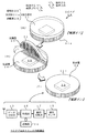
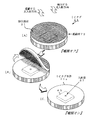
図1は、第1の実施形態におけるICタグ11を示す図である。
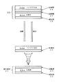
図2は、ICタグ11の層構造を示す図である。
このICタグ11は、ICタグ本体11aと接合部材21とを接合して構成される。
<< First Embodiment >>
FIG. 1 is a diagram illustrating an
FIG. 2 is a diagram showing the layer structure of the
The
[ICタグ本体11aの構成説明]
図1に示すICタグ本体11aは、下記のユニットを内蔵する。
(1)データ通信部13・・電波や赤外線などを用いてデータ通信を行う。
(2)記録部14・・通常のタグ動作に必要なプログラムやデータの他に、外部からの動作モードの切り換えに必要なプログラムやデータも記録可能である。
(3)磁気センサ15・・ICタグ本体11aの接合面に対して垂直方向の磁界を検出するセンサ。例えば、強磁性体磁気抵抗素子(強磁性体の磁気抵抗効果を利用し、磁界強度により抵抗値が変化するセンサ)やリードスイッチなど。
(4)処理部16・・データ通信部13および記録部14を制御する。
(5)動作切換部17・・磁気センサ15の検出結果に応じてICタグ本体11aの動作モードを切り換える。
(6)粘着層24・・ICタグ本体11aの接合面に設けられた粘着剤の層。
[Description of Configuration of IC Tag Body 11a]
The IC tag main body 11a shown in FIG. 1 incorporates the following units.
(1) Data communication unit 13 .. Data communication is performed using radio waves or infrared rays.
(2) Recording unit 14... In addition to programs and data necessary for normal tag operation, programs and data necessary for switching operation modes from the outside can be recorded.
(3)
(4) Control the processing unit 16... The data communication unit 13 and the recording unit 14.
(5)
(6)
[接合部材21の構成説明]
一方、接合部材21は、下記の層を備える。
(1)剥離層23・・粘着層24と剥離可能な状態で接合する層。さらに、この剥離層23は、ICタグ本体11aの粘着層24をカバーすることで、埃やゴミの付着を防止する機能を有する。
(2)磁性体22・・ICタグ本体11aの接合面に対して垂直方向に磁界を印加する層。さらに、この磁性体22は、ICタグ本体11aへの磁界印加により、ICタグ本体11aの動作モードを切り換える機能を有する。
(3)支持体21a・・接合部材21の機械的強度を担うシートであり、剥離層23および磁性体22を支持する。さらに、支持体21aは、ICタグ本体11aを運搬時の機械的衝撃から保護する機能も有する。
[Description of Configuration of Joining Member 21]
On the other hand, the joining
(1)
(2)
(3) Support body 21 a... Sheet that bears the mechanical strength of the joining
[動作説明]
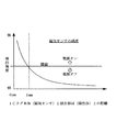
図3は、ICタグ本体11aと接合部材21との距離と、磁気センサ15による磁界の検出強度との関係を説明する図である。
この図3では、両者の距離が1mm未満になると、磁気センサ15の検出強度が累進的に高くなる。一方、両者の距離が1mm以上になると、磁気センサ15の検出強度が顕著に小さくなる。そこで、距離1mmの時の検出強度を閾値に設定することにより、磁気センサ15を用いて、接合部材21の有無を的確に判定することができる。
[Description of operation]
FIG. 3 is a diagram for explaining the relationship between the distance between the IC tag main body 11a and the
In FIG. 3, when the distance between the two becomes less than 1 mm, the detection intensity of the
すなわち、磁界の検出強度が閾値以上の場合、ICタグ本体11aと接合部材21との距離は1mm未満であり、両者は図1[A]に示すような接合状態にあると判定できる。この場合、動作切換部17は、ICタグ本体11aを電源オフに維持する。したがって、接合部材21を接合したICタグ本体11aは、電力消費が僅かとなり、ICタグ本体11aの実使用可能な期間を延ばすことができる。
That is, when the detected intensity of the magnetic field is equal to or greater than the threshold, the distance between the IC tag main body 11a and the
一方、磁界の検出強度が閾値未満の場合、ICタグ本体11aと接合部材21との距離は1mm以上であり、両者は図1[C]に示すような剥離状態にあると判定できる。この場合、動作切換部17は、ICタグ本体11aを電源オンに切り換える。したがって、ICタグ本体11aから接合部材21を、シールのように剥がすことによって、ICタグ本体11aの動作を開始させることができる。
On the other hand, when the detected intensity of the magnetic field is less than the threshold value, the distance between the IC tag main body 11a and the
さらに、この接合部材21を剥がすことによって、ICタグ本体11aの接合面には粘着層24が現れる。そのため、そのままICタグ本体11aを商品などに貼り付けることが可能になる。
次に、別の実施形態について説明する。
Furthermore, the
Next, another embodiment will be described.
《第2の実施形態》
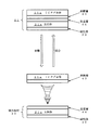
図4は、第2の実施形態におけるICタグの層構成を示す図である。
第2の実施形態の特徴は、ICタグ本体11aの接合面に剥離層43を設け、接合部材21側に粘着層44を設けている点である。なお、その他の構成は、第1の実施形態(図1,図2)と同じため、ここでの説明を省略する。
このような構成においても、接合部材21を剥がすことによって、ICタグ本体11aを電源オフ状態から電源オン状態に切り換えることができる。
<< Second Embodiment >>
FIG. 4 is a diagram showing a layer configuration of the IC tag in the second embodiment.
A feature of the second embodiment is that a peeling layer 43 is provided on the joining surface of the IC tag main body 11a, and an adhesive layer 44 is provided on the joining
Even in such a configuration, the IC tag main body 11a can be switched from the power-off state to the power-on state by peeling off the joining
さらに、本実施形態では、接合部材21(粘着層44)が剥離後も接着機能を有する。そのため、ICタグ本体11aに接合部材21を再び貼り付けることが可能となり、ICタグ本体11aを再び電源オフ状態に切り換えることができる。
したがって、未使用時のICタグ本体11aを随時に電源オフ状態にして保管することが可能になり、ICタグ本体11aの実使用可能な期間を更に延ばすことができる。
次に、別の実施形態について説明する。
Furthermore, in this embodiment, the bonding member 21 (adhesive layer 44) has an adhesive function even after peeling. Therefore, the joining
Therefore, the IC tag main body 11a when not in use can be stored with the power turned off at any time, and the usable period of the IC tag main body 11a can be further extended.
Next, another embodiment will be described.
《第3の実施形態》
図5は、第3の実施形態におけるICタグの層構成を示す図である。
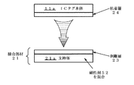
第3の実施形態の特徴は、支持体21aに磁性剤52を混合した後、外部磁界をかけて磁性剤52の磁化方向を所望の向きに配向している点である。このような構成により、支持体21aに磁性体の機能を持たせることができる。その結果、接合部材21の層数が減り、接合部材21の厚さを薄くすることができる。
次に、別の実施形態について説明する。
<< Third Embodiment >>
FIG. 5 is a diagram showing a layer structure of the IC tag in the third embodiment.
A feature of the third embodiment is that after the magnetic agent 52 is mixed with the support 21a, an external magnetic field is applied to orient the magnetization direction of the magnetic agent 52 in a desired direction. With this configuration, the support 21a can have a magnetic function. As a result, the number of layers of the
Next, another embodiment will be described.
《第4の実施形態》
図6は、第4の実施形態におけるICタグの層構成を示す図である。
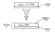
第4の実施形態の特徴は、支持体21aに剥離剤53を混合することにより、支持体21aに剥離層の機能を持たせている点である。その結果、接合部材21の層数が減り、接合部材21の厚さを薄くすることができる。
次に、別の実施形態について説明する。
<< Fourth Embodiment >>
FIG. 6 is a diagram illustrating a layer configuration of an IC tag according to the fourth embodiment.
The feature of 4th Embodiment is the point which makes the support body 21a the function of a peeling layer by mixing the peeling agent 53 with the support body 21a. As a result, the number of layers of the
Next, another embodiment will be described.
《第5の実施形態》
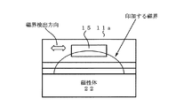
図7は、第5の実施形態における磁性体22の磁界印加方向を示す図である。
第5の実施形態では、磁性体22に垂直磁化を与えることにより、垂直方向に磁界を発生させる。その一方、磁気センサ15は、磁界検出方向が垂直方向に設定される。
したがって、磁性体22および磁気センサ15の指向性が一致するため、磁気センサ15の感度を一段と高めることができる。
次に、別の実施形態について説明する。
<< Fifth Embodiment >>
FIG. 7 is a diagram illustrating the magnetic field application direction of the
In the fifth embodiment, a magnetic field is generated in the vertical direction by applying perpendicular magnetization to the
Therefore, since the directivities of the
Next, another embodiment will be described.
《第6の実施形態》
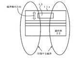
図8は、第6の実施形態における磁性体22の磁界印加方向を示す図である。
第6の実施形態では、磁性体22に水平方向の磁化を与えることにより、水平方向の磁界を発生させる。一方、磁気センサ15は、磁界検出方向が水平方向に設定される。
したがって、磁性体22および磁気センサ15の指向性が一致するため、磁気センサ15の感度を一段と高めることができる。
次に、別の実施形態について説明する。
<< Sixth Embodiment >>
FIG. 8 is a diagram showing the magnetic field application direction of the
In the sixth embodiment, a horizontal magnetic field is generated by applying horizontal magnetization to the
Therefore, since the directivities of the
Next, another embodiment will be described.
《第7の実施形態》
図9は、第7の実施形態におけるICタグを示す図である。
第7の実施形態の特徴は、磁気センサ15に代えて、光センサ65をICタグ本体11aに設ける。この光センサ65は、ICタグ本体11aの接合面に設けた入射窓67から、光を検出する。さらに、磁性体22に代えて遮蔽材72を接合部材21に設ける。
<< Seventh Embodiment >>
FIG. 9 is a diagram showing an IC tag according to the seventh embodiment.
A feature of the seventh embodiment is that an
なお、粘着層や剥離層の構成については、その他の実施形態と共通するため、ここでの説明を省略する。
第7の実施形態では、接合部材21をICタグ本体11aに接合することにより、入射窓67を塞ぎ、光センサ65を遮蔽状態に保つ。光センサ65は、この遮蔽状態を光電出力の信号レベルから検出することにより、図9[A]に示すような接合状態にあると判定する。
In addition, about the structure of an adhesion layer or a peeling layer, since it is common with other embodiment, description here is abbreviate | omitted.
In the seventh embodiment, the joining
この場合、動作切換部17は、ICタグ本体11aを電源オフに維持する。したがって、接合部材21を接合したICタグ本体11aは、電源オフ状態を維持して電力消費が僅かとなり、ICタグ本体11aの実使用可能な期間を延ばすことができる。
一方、接合部材21をICタグ本体11aから剥がすことにより、接合面の入射窓67が露出し、光センサ65に光が入射する。光センサ65は、この状態を光電出力の信号レベルから検出すると、図9[C]に示すような剥離状態にあると判定する。
In this case, the
On the other hand, by peeling the
この場合、動作切換部17は、ICタグ本体11aを電源オンに切り換える。したがって、ICタグ本体11aから接合部材21を、シールのように剥がすことによって、ICタグ本体11aの動作を開始させることができる。
なお、ICタグ本体11aの使用中に、たまたま入射窓67が暗くなることで電源オフしてはまずい場合もある。この場合は、動作切換部17が、光電出力の信号レベル低下が上限回数(例えば1〜2回程度)を超えた段階で、電源オフへの切り換えを打ち切ればよい。
In this case, the
In addition, while the IC tag main body 11a is being used, there is a case where the power is turned off because the incident window 67 happens to be dark. In this case, the
《実施形態の補足事項》
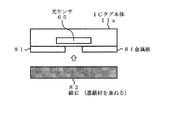
なお、上述した実施形態では、粘着層および剥離層を用いて、ICタグ本体11aと接合部材21とを着脱可能に接合する場合について説明した。しかしながら、本発明はこれに限定されるものではない。例えば、図10に示すように、金属板81および磁石82を用いて、ICタグ本体11aと接合部材21とを接合してもよい。また、マジックテープ(登録商標)や係止部材その他の着脱可能な着脱部を用いて、ICタグ本体11aと接合部材21とを接合してもよい。
<< Additional items of embodiment >>
In the above-described embodiment, the case where the IC tag main body 11a and the
なお、上述した実施形態では、接合部材21の着脱により、ICタグ本体11aの電源オン/電源オフを切り換える場合について説明した。しかしながら、本発明はこれに限定されるものではない。例えば、電源オフ(いわゆる休止モード)の代わりに省電力モードに切り換えてもよい。また例えば、外界状態の検出/非検出に応じて、所望の動作モード切り換えを行ってもよい。
In the above-described embodiment, the case where the power ON / OFF of the IC tag main body 11a is switched by attaching / detaching the joining
また、上述した実施形態では、接合部材21をICタグ本体11aに接合することで、ICタグ本体11aを電源オフしている。しかしながら、本発明はこれに限定されるものではない。例えば、逆に、接合部材21をICタグ本体11aに接合することで、ICタグ本体11aを電源オンしてもよい。
In the above-described embodiment, the IC tag body 11a is powered off by joining the joining
なお、上述した実施形態では、磁気センサまたは光センサの場合について説明している。しかしながら、本発明はこれに限定されるものではない。より一般的には、ICタグ本体の内蔵するセンサの仕様に対応して、センサに予め定められた外界状態を検出させる物理量印加部を接合部材に設ければよい。例えば、次のようなセンサと物理量印加部の組み合わせが好ましい。 In the above-described embodiment, the case of a magnetic sensor or an optical sensor has been described. However, the present invention is not limited to this. More generally, the bonding member may be provided with a physical quantity application unit that allows the sensor to detect a predetermined external state corresponding to the specification of the sensor built in the IC tag body. For example, the following combinations of sensors and physical quantity application units are preferable.
(1)電界センサ/電界印加部
(2)光センサ/発光部,遮光部材,偏光部材,カラーフィルタ
(3)静電容量センサ/誘電体の接触機構,外部電極
(4)圧電センサ/圧力印加機構
(5)圧力センサ/圧力印加機構
(6)接触センサ/接触機構
(7)電磁波センサ/電磁波ノイズの発生機構など
(8)電圧センサ/電圧印加機構
(9)リードスイッチ/磁石、電磁石
(10)受光素子としての太陽電池/発光部,遮光部材,偏光部材,カラーフィルタ
(11)温度センサ/発熱機構または冷却機構
(12)気圧センサ/気密性の容器と空気ポンプなど
(13)ガスセンサ/気密性の容器と特定ガス発生機構
(14)加速度センサ/遠心力発生機構,振動機構
(15)歪みセンサ/歪み発生機構,圧力印加機構
(16)音センサ/音源
(1) Electric field sensor / electric field application part (2) Optical sensor / light emitting part, light shielding member, polarizing member, color filter (3) Capacitance sensor / dielectric contact mechanism, external electrode (4) Piezoelectric sensor / pressure application Mechanism (5) Pressure sensor / pressure application mechanism (6) Contact sensor / contact mechanism (7) Electromagnetic sensor / electromagnetic noise generation mechanism, etc. (8) Voltage sensor / voltage application mechanism (9) Reed switch / magnet, electromagnet (10 ) Solar cell / light emitting part as light receiving element, light shielding member, polarizing member, color filter (11) Temperature sensor / heating mechanism or cooling mechanism (12) Pressure sensor / airtight container and air pump, etc. (13) Gas sensor / airtightness Container and specific gas generation mechanism (14) acceleration sensor / centrifugal force generation mechanism, vibration mechanism (15) strain sensor / strain generation mechanism, pressure application mechanism (16) sound sensor / sound source
なお、上述した実施形態では、タグ形状のICタグについて説明した。しかしながら、本発明はこれに限定されるものではない。例えば、ICカードに本発明を適用してもよい。 In the above-described embodiment, the tag-shaped IC tag has been described. However, the present invention is not limited to this. For example, the present invention may be applied to an IC card.
以上説明したように、本発明は、ICタグに利用可能な技術である。 As described above, the present invention is a technique that can be used for an IC tag.
11 ICタグ
11a ICタグ本体
15 磁気センサ
17 動作切換部
21 接合部材
21a 支持体
22 磁性体
23 剥離層
24 粘着層
43 剥離層
44 粘着層
52 磁性剤
53 剥離剤
65 光センサ
67 入射窓
72 遮蔽材
81 金属板
82 磁石
DESCRIPTION OF
Claims (10)
前記ICタグ本体は、
前記ICタグの動作を実行する処理部と、
外部操作可能な所定の物理量を外界からセンシングして、予め定められた外界状態を検出するセンサと、
前記センサによる前記外界状態の検出/非検出に応じて動作モードを切り換える動作切換部と
を備え、
前記接合部材は、
前記ICタグ本体に着脱可能な着脱部と、
前記接合部材を前記ICタグ本体に接合した状態で、前記ICタグ本体に前記外界状態を与えることにより、前記ICタグ本体の前記動作モードを維持する物理量印加部とを備えた
ことを特徴とするICタグ。 An IC tag comprising an IC tag body and a joining member joined to the IC tag body,
The IC tag body is
A processing unit for performing the operation of the IC tag;
A sensor that senses a predetermined physical quantity that can be externally operated from the outside world and detects a predetermined outside world state,
An operation switching unit that switches an operation mode according to detection / non-detection of the external state by the sensor,
The joining member is
A detachable part detachable from the IC tag body;
A physical quantity application unit that maintains the operation mode of the IC tag main body by giving the external state to the IC tag main body in a state where the bonding member is bonded to the IC tag main body. IC tag.
前記物理量印加部は、
前記ICタグ本体を、省電力モードおよび休止モードの一方に維持する前記外界状態を、前記ICタグに与えることにより、前記接合部材を接合した状態の前記ICタグ本体の電力消費を削減する
ことを特徴とするICタグ。 The IC tag according to claim 1,
The physical quantity application unit includes:
Reducing the power consumption of the IC tag body in a state in which the joining member is joined by providing the IC tag with the external state that maintains the IC tag body in one of a power saving mode and a sleep mode. Characteristic IC tag.
前記ICタグ本体は、前記接合部材を剥離した箇所に、剥離層を備え、
前記接合部材の前記着脱部は、剥離後も接着機能を有する粘着層である
ことを特徴とするICタグ。 In the IC tag according to claim 1 or 2,
The IC tag body includes a release layer at a location where the bonding member is peeled off,
The IC tag, wherein the attaching / detaching portion of the joining member is an adhesive layer having an adhesive function even after peeling.
前記ICタグ本体は、前記接合部材を剥離した箇所に、接着機能を有する粘着層を備える
ことを特徴とするICタグ。 In the IC tag according to claim 1 or 2,
The IC tag main body includes an adhesive layer having an adhesive function at a position where the joining member is peeled off.
前記接合部材は、
支持体と、
前記支持体に剥離剤を混合して構成される剥離層とを備えた
ことを特徴とするICタグ。 The IC tag according to claim 4,
The joining member is
A support;
An IC tag comprising: a release layer configured by mixing a release agent with the support.
前記接合部材は、支持体を備え、
前記物理量印加部は、前記支持体に混合されている
ことを特徴とするICタグ。 In the IC tag according to any one of claims 1 to 5,
The joining member includes a support,
The IC tag, wherein the physical quantity application unit is mixed with the support.
前記ICタグ本体の前記センサは、前記物理量のセンシングに指向性を有し、
前記物理量印加部は、前記物理量の印加方向に指向性を有し、
前記接合部材を前記ICタグ本体に接合した状態で、両者の前記指向性が一致する
ことを特徴とするICタグ。 In the IC tag according to any one of claims 1 to 6,
The sensor of the IC tag body has directivity for sensing the physical quantity,
The physical quantity application unit has directivity in the application direction of the physical quantity,
An IC tag, wherein the directivities of the two match when the joining member is joined to the IC tag main body.
前記接合部材と前記ICタグ本体とを1mm以上離した状態では、前記ICタグ本体の前記センサが前記外界状態を検出しないように、『前記物理量印加部の前記物理量の空間強度』および/または『前記センサの感度』が設定される
ことを特徴とするICタグ。 The IC tag according to any one of claims 1 to 7,
In a state where the joining member and the IC tag main body are separated by 1 mm or more, “the spatial intensity of the physical quantity of the physical quantity application unit” and / or “so that the sensor of the IC tag main body does not detect the external state”. The sensitivity of the sensor is set.
前記ICタグ本体の前記センサは、磁界を検出する磁気センサであり、
前記着脱部の前記物理量印加部は、磁界を発生させる磁性材である
ことを特徴とするICタグ。 In the IC tag according to any one of claims 1 to 8,
The sensor of the IC tag body is a magnetic sensor for detecting a magnetic field,
The IC tag, wherein the physical quantity application unit of the detachable unit is a magnetic material that generates a magnetic field.
前記ICタグ本体の前記センサは、光を検出する光センサであり、
前記接合部材の前記物理量印加部は、光を減光または遮蔽する遮蔽材である
ことを特徴とするICタグ。 In the IC tag according to any one of claims 1 to 8,
The sensor of the IC tag body is an optical sensor that detects light,
The IC tag, wherein the physical quantity application unit of the joining member is a shielding material that reduces or shields light.
Priority Applications (1)
| Application Number | Priority Date | Filing Date | Title |
|---|---|---|---|
| JP2004111182A JP4393909B2 (en) | 2004-04-05 | 2004-04-05 | IC tag |
Applications Claiming Priority (1)
| Application Number | Priority Date | Filing Date | Title |
|---|---|---|---|
| JP2004111182A JP4393909B2 (en) | 2004-04-05 | 2004-04-05 | IC tag |
Publications (2)
| Publication Number | Publication Date |
|---|---|
| JP2005293486A true JP2005293486A (en) | 2005-10-20 |
| JP4393909B2 JP4393909B2 (en) | 2010-01-06 |
Family
ID=35326311
Family Applications (1)
| Application Number | Title | Priority Date | Filing Date |
|---|---|---|---|
| JP2004111182A Expired - Fee Related JP4393909B2 (en) | 2004-04-05 | 2004-04-05 | IC tag |
Country Status (1)
| Country | Link |
|---|---|
| JP (1) | JP4393909B2 (en) |
Cited By (6)
| Publication number | Priority date | Publication date | Assignee | Title |
|---|---|---|---|---|
| JP2007241651A (en) * | 2006-03-08 | 2007-09-20 | Terumo Corp | Ic tag |
| JP2009025144A (en) * | 2007-07-19 | 2009-02-05 | Sanko Gosei Ltd | Sample storage container and blood collection container |
| JP2012114019A (en) * | 2010-11-26 | 2012-06-14 | Sony Corp | Secondary battery cell, battery pack and power consuming apparatus |
| JP2016024507A (en) * | 2014-07-16 | 2016-02-08 | 株式会社富士通アドバンストエンジニアリング | Detection device, detection device starting method and detection device starting program |
| JP2019079559A (en) * | 2019-01-11 | 2019-05-23 | 新コスモス電機株式会社 | Alarm |
| JP2021147056A (en) * | 2020-03-16 | 2021-09-27 | ホシデン株式会社 | Id tag device and method of driving the same |
-
2004
- 2004-04-05 JP JP2004111182A patent/JP4393909B2/en not_active Expired - Fee Related
Cited By (7)
| Publication number | Priority date | Publication date | Assignee | Title |
|---|---|---|---|---|
| JP2007241651A (en) * | 2006-03-08 | 2007-09-20 | Terumo Corp | Ic tag |
| JP2009025144A (en) * | 2007-07-19 | 2009-02-05 | Sanko Gosei Ltd | Sample storage container and blood collection container |
| JP2012114019A (en) * | 2010-11-26 | 2012-06-14 | Sony Corp | Secondary battery cell, battery pack and power consuming apparatus |
| JP2016024507A (en) * | 2014-07-16 | 2016-02-08 | 株式会社富士通アドバンストエンジニアリング | Detection device, detection device starting method and detection device starting program |
| JP2019079559A (en) * | 2019-01-11 | 2019-05-23 | 新コスモス電機株式会社 | Alarm |
| JP2021147056A (en) * | 2020-03-16 | 2021-09-27 | ホシデン株式会社 | Id tag device and method of driving the same |
| JP7426860B2 (en) | 2020-03-16 | 2024-02-02 | ホシデン株式会社 | ID tag device and its driving method |
Also Published As
| Publication number | Publication date |
|---|---|
| JP4393909B2 (en) | 2010-01-06 |
Similar Documents
| Publication | Publication Date | Title |
|---|---|---|
| JP2005293485A (en) | Ic tag | |
| US8604905B2 (en) | Finger biometric sensor including laterally adjacent piezoelectric transducer layer and associated methods | |
| US9224516B2 (en) | Battery tab and packaging frame design | |
| JP3557990B2 (en) | Information recording tag | |
| US10990864B2 (en) | Liquid metal-based information identification system | |
| US11614777B2 (en) | Electronic apparatus and method for manufacturing the same | |
| CN103400181B (en) | Finger print reading sensor IC-card and method for packing thereof | |
| JP4393909B2 (en) | IC tag | |
| TWI741663B (en) | Wearable device and earbud | |
| US8646696B2 (en) | Chip card comprising a display | |
| CN102855516A (en) | Anti-theft electronic tag | |
| CN207408978U (en) | Paste the anti-dismounting structure of the type active RFID electronic label of class | |
| US20180170030A1 (en) | Electronic apparatus and disassembling method therefor | |
| CN110989838A (en) | Wearable device, control method thereof, and computer-readable storage medium | |
| TW201250254A (en) | Signal processing circuit, oscillation detection circuit and electronic device | |
| CN110096127A (en) | A kind of switching device and its control method for wireless vehicle detector | |
| JP2004170308A (en) | Pressure sensitive device | |
| KR20210077609A (en) | System and method for utilizing pressure sensors in an electric device | |
| JP2005293484A (en) | Storage container for ic tag | |
| JP7752679B2 (en) | Temperature indicator | |
| CN212909477U (en) | Pressure button and electronic equipment | |
| CN221040058U (en) | Magnetic recyclable RFID tag device for the furniture industry | |
| CN113063528A (en) | Sealing structure of pressure gauge | |
| CN223486479U (en) | Touch screen integrated with piezoelectric transducer and electronic equipment | |
| CN217821641U (en) | Waterproof positioning label |
Legal Events
| Date | Code | Title | Description |
|---|---|---|---|
| A621 | Written request for application examination |
Free format text: JAPANESE INTERMEDIATE CODE: A621 Effective date: 20060815 |
|
| A977 | Report on retrieval |
Free format text: JAPANESE INTERMEDIATE CODE: A971007 Effective date: 20090605 |
|
| A131 | Notification of reasons for refusal |
Free format text: JAPANESE INTERMEDIATE CODE: A131 Effective date: 20090728 |
|
| A521 | Written amendment |
Free format text: JAPANESE INTERMEDIATE CODE: A523 Effective date: 20090915 |
|
| TRDD | Decision of grant or rejection written | ||
| A01 | Written decision to grant a patent or to grant a registration (utility model) |
Free format text: JAPANESE INTERMEDIATE CODE: A01 Effective date: 20091013 |
|
| A01 | Written decision to grant a patent or to grant a registration (utility model) |
Free format text: JAPANESE INTERMEDIATE CODE: A01 |
|
| A61 | First payment of annual fees (during grant procedure) |
Free format text: JAPANESE INTERMEDIATE CODE: A61 Effective date: 20091014 |
|
| R150 | Certificate of patent (=grant) or registration of utility model |
Free format text: JAPANESE INTERMEDIATE CODE: R150 |
|
| FPAY | Renewal fee payment (prs date is renewal date of database) |
Free format text: PAYMENT UNTIL: 20121023 Year of fee payment: 3 |
|
| FPAY | Renewal fee payment (prs date is renewal date of database) |
Free format text: PAYMENT UNTIL: 20121023 Year of fee payment: 3 |
|
| FPAY | Renewal fee payment (prs date is renewal date of database) |
Free format text: PAYMENT UNTIL: 20131023 Year of fee payment: 4 |
|
| S531 | Written request for registration of change of domicile |
Free format text: JAPANESE INTERMEDIATE CODE: R313531 |
|
| R350 | Written notification of registration of transfer |
Free format text: JAPANESE INTERMEDIATE CODE: R350 |
|
| LAPS | Cancellation because of no payment of annual fees |